Note: Descriptions are shown in the official language in which they were submitted.
, CA 02784815 2012-08-03
,
1
Power contact device with electrodynamic compensation in the
presence of high currents.
Background of the invention
The invention relates to a power contact device of an electric control
apparatus comprising:
- at least a first stationary contact element and a second movable contact
element designed to occupy a closed position in which they are in electric
contact for establishment and flow of the current, and an open position in
which the two contact elements are separated from one another interrupting
flow of the current,
- and electrodynamic compensation means for keeping the contact
elements in the closed position when a short-circuit current occurs, said
compensation being performed by means of the electrodynamic attraction
effect due to flow of the current taking place in the same direction in the
two
contact elements.
The electric control apparatus does not have any breaking capacity but its
contacts must imperatively remain closed in the presence of a short-circuit,
which is eliminated by a protective circuit breaker connected line-side.
State of the art
To guarantee this immunity of the contacts when a short-circuit occurs, it is
known to compensate the electrodynamic repulsion force exerted between
the contacts by an opposing electrodynamic force exerted in the opposite
direction.
The force exerted on the movable contact is directly proportional to the
square of the current, but inversely proportional to the distance between the
CA 02784815 2012-08-03
2
contacts. This distance must not be too large to have a significant effect on
small or medium over-currents. In the case of large short-circuit currents on
the other hand, the electrodynamic forces are high and could deform copper
contact parts.
The document FR2905795 concerns a contact device comprising two
separable contact elements extending in parallel manner to one another in
the closed position, each being equipped with a pair of contact pads. In the
closed position, the two contact elements are arranged facing one another,
and are electrically connected in parallel, so that the current is shared
between the two contact elements, flowing in the same direction in the latter.
This results in electrodynamic attraction forces which keep the contact pads
closed. These forces are not affected by a possible magnetic circuit
saturation, as everything takes place in air. On large short-circuit currents,
the attraction forces are very high and could deform contact elements with
elongate branches. Such a contact device further requires two contact pads
per contact element, which increases the manufacturing cost.
Another known solution consists in making use of a U-shaped magnetic
circuit to keep the contacts closed. This results in limitation of the
attraction
forces due to saturation, but the volume of the current interruption chambers
is increased.
Object of the invention
The object of the invention consists in providing a power contact device of
small size with improved electrodynamic compensation independently from
the current intensity.
The contact device according to the invention is characterized in that the two
stationary and movable contact elements are in the form of two juxtaposed
coiled turns arranged facing one another in the open position, each turn
3
being made from a material that is both magnetic and current conducting to
constitute a single part acting as power contact, as coil generating a
magnetic
induction field, and as magnetic circuit performing reinforcing and
channelling
of said magnetic field.
Preferred embodiments of the invention are described hereunder.
In the closed position, when the current flows from the movable contact
element
to the stationary contact element, a coil is obtained with two turns in
series,
resulting in formation of a magnetic field channelled by the turns themselves,
since they also act as magnetic circuit. This results in electro-dynamic
attraction
forces between the mobile turn and the fixed turn which keep the contacts
closed in the case of a short-circuit or overcurrent. Such a contact device
requires few parts to obtain the desired compensation force. The two turns
further enable limiting of the electrodynamic forces following saturation of
the
magnetic material, which prevents deformation of the contact elements on
strong currents.
The electric control apparatus can be a power switch, a contactor, or a
reversing
switch.
According to one feature of the invention, the first contact element and the
second contact element are made either from a steel metallic material or by
sintering of a magnetic metal powder with a thermoplastic binder.
According to another feature of the invention, the two coiled turns of the
first
stationary contact element and of the second movable contact element extend
in two parallel planes in the open position, the second movable contact
element
being mounted pivotally on a vertical axis.
According to a preferred embodiment, the second movable contact element is
inserted between the first stationary contact element and a third stationary
contact element to constitute a current-reversing contact device with two
closed positions situated on each side of the median open position. The third
CA 2784815 2018-11-23
CA 02784815 2012-08-03
4
stationary contact element is in the shape of a coiled turn made from the
same material as that of the coiled turn of the first stationary contact
element,
and extending in parallel manner to the latter.
Such a contact device is applied to a three-phase reversing switch enabling
the direction of rotation of a three-phase electric motor to be reversed by
reversing the connection between two phases. The contacts of this reversing
switch remain closed in the presence of a short-circuit.
The poles of the reversing switch are housed in three juxtaposed
compartments of a case made from insulating material, in which:
- the first stationary contacts of the two end poles are electrically
inter-
connected by a first connecting conductor in connection with a. first
connection terminal,
- the third stationary contacts of the two end poles are interconnected
by a
second connecting conductor in connection with a third connection terminal.
The two connecting conductors are parallel and insulated from one another,
and a pass-through conductor without a current interruption gap is
advantageously integrated in the intermediate pole.
Brief description of the drawings
Other advantages and features will become more clearly apparent from the
following description of an embodiment of the invention given for non-
restrictive example purposes only and represented in the appended
drawings, in which:
- figure 1 is an exploded perspective view of a contact device according to
the invention, comprising a single stationary contact element;
CA 02784815 2012-08-03
- figure 2 represents an identical view of an alternative embodiment of the
invention with a double contact device equipped with a pair of stationary,
contacts of reversing switch type;
- figure 3 shows a contact device of two end poles of a three-phase
reversing switch using the contact device of figure 2 in each pole;
- figure 4 represents a contact device with the three poles of a three-phase
reversing switch, which uses the contact device of figure 3, with in
addition a pass-through conductor integrated in the intermediate pole;
- figure 5 is an exploded perspective view of a three-phase reversing
switch the poles of which are housed in three juxtaposed compartments
of a case made from insulating material.
Detailed description of the invention
In figure 1, a power contact device 10 for an electric control apparatus
comprises a first stationary contact element 11 and a second movable
contact element 12. The latter is mounted pivoting around a vertical axis XX'
delineated by two opposite ends 13, 14 aligned in the vertical direction. The
first stationary contact element 11 is provided with a contact pad 15 arranged
facing another contact pad 16 securedly affixed to second movable contact
element 12. The two contact pads 15, 16 are able to occupy either a closed
position in which they are in electric contact for establishment and flow of
the
current, or an open position in which contact pad 16 separates from the other
contact pad 15 after pivoting of second movable contact element 12. This
separation of the contacts interrupts flow of the current.
The opening and closing operations of contact device 10 are performed by
means of an operating mechanism (not shown) housed in the case of the
electric apparatus. This control function apparatus, in particular of switch,
contactor, or reversing switch type, does not have any breaking capacity, and
contact elements 11, 12 absolutely must remain in the closed position in the
CA 02784815 2012-08-03
6
presence of a high-intensity current liable to generate electrodynamic
repulsion forces between contact pads 15, 16.
To compensate these repulsion forces in the event of an overcurrent,
stationary contact element 11 and mobile contact element 12 are both in the
form of a coiled turn made from a material that is both magnetic and current
conducting. For example purposes, this material can be made from steel by
increasing the cross-section with respect to a conventional copper conductor
for reasons of overheating.
to
It can also be produced by the MIM method consisting in mixing fine
magnetic metallic powder with a thermoplastic binder in order to obtain
granules of material able to be transformed by thermoplastic moulding. The
part obtained in this way is placed in a furnace to eliminate the
thermoplastic
binder, which escapes in the form of gas. The temperature increase of the
furnace enables sintering of the part to be obtained giving the latter the
cohesion and structure of a metal part.
The two coiled turns of first stationary contact element 11 and of second
movable contact element 12 extend in two parallel planes in the open
position, being separated from one another by a reduced isolating distance
suitable for a good dielectric strength. Each coiled turn presents a bottom
branch 17 and a top branch 18 which are separated from one another by an
elongate slot 19 which extends orthogonally to the vertical direction of the
axis XX' of pivoting of second movable contact element 12.
Each coiled turn, made from magnetic current conducting material, forms a
single part playing the combined role of power contact, of coil generating a
magnetic induction field, and of magnetic circuit reinforcing and channelling
said magnetic field.
CA 02784815 2012-08-03
7
In figure 1 which shows an exploded perspective view of contact device 10, it
can be imagined that the two contact elements 11, 12 are in electric contact
via their contact pads 15, 16. The broken line TR symbolizes flow of the
current in the closed position when contact pad 16 is in engagement against
stationary contact pad 15. It can be noted that the direction of current flow
is
the same in the bottom branches 17 of the two loops. The same is the case
in the two top branches 18 of the two loops. Such a current flow causes an
electrodynamic attraction effect between the two loops when a short-circuit
current occurs. Attraction forces Fl and F2 are proportional to the square of
-to the current, and enable the repulsion forces exerted at the level of
contact
pads 15, 16 by the same current to be compensated. Maintaining of contact
elements 11, 12 in the closed position is thus guaranteed in the presence of
a short-circuit current. The latter is eliminated after operation of a
protective
circuit breaker placed line-side with respect to the power supply source.
Attraction forces Fl and F2 are further reinforced by the magnetic circuit
formed by the two adjacent magnetic material loops. This magnetic circuit
channels and concentrates the force lines of the magnetic field generated by
the coil of the two coiled turns in series, so as to obtain an optimal
attraction
effect.
Such a structure with electrodynamic compensation of contact device 10 can
be fitted in any electric apparatus that does not have to react in the
presence
of a short-circuit current, in particular a switch, a contactor or a reversing
switch.
With reference to figure 2, the same reference numerals will be used to
designate similar parts to those of contact device 10 of figure 1. Second
movable contact element 12 is inserted between first stationary contact
element 11 and a third stationary contact element 20 to form a current-
reversing contact device 100 with two closed positions situated on each side
of the median open position. Third stationary contact element 20 is in the
= CA 02784815 2012-08-03
8
form of a coiled turn made from the same material as that of the coiled turn
of
first stationary contact element 11 and extending in parallel manner to the
latter. Contact pad 16 of second movable contact element 12 can come into
contact either with contact pad 15 of first stationary contact element 11 or
with contact pad 21 of third stationary contact element 20 (shown in a broken
line).
It can be imagined in figure 2 that the two contact elements 11, 12 are in
electric contact via their contact pads 15, 16. The broken line TR symbolizes
flow of the current in the closed position, and the direction of current flow
is
identical to that of figure 1, with the same attraction forces Fl and F2 for
electrodynamic compensation. In the other state of reversing-switch contact
device 100, second movable contact element 12 pivots in the revere direction
so that contact pad 16 comes into engagement against contact pad 21 of
third stationary contact element 20. In this case a coil with two coiled turns
in
series is also to be found, with the same electrodynamic attraction forces for
holding in the closed position.
Figure 3 shows contact device 200 of two end poles R,T of a three-phase
reversing switch, using contact device 100 of figure 2 in each pole.
First stationary contact elements 11 of the two end poles R,T are electrically
interconnected by a first connecting conductor 22 connected with a first
connection terminal Bl.
Third stationary contact elements 20 of the two end poles R,T are
interconnected by a second connecting conductor 23 connected with third
connection terminal B3.
The two connecting conductors 22, 23 are parallel and insulated from one
another.
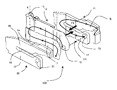
Figure 4 represents a contact device 300 with the three poles R,S,T of a
three-phase reversing switch, which uses contact device 200 of figure 3, with
in addition a pass-through conductor 24 without a current interruption gap
CA 02784815 2012-08-03
9
integrated in intermediate pole S. This conductor 24 is formed by a
continuous contact part connected with a second connection terminal B2,
which is arranged between first and third terminals 61, B2 of the reversing
switch.
Figure 5 is an exploded perspective view of a three-phase reversing switch
the poles R,S,T of which are housed in three juxtaposed compartments of a
case 25 made from insulating material. The compartments are insulated from
one another by vertical separating walls 26, and contact device 200 is
inserted in the end poles R,T via the top of the case 25 which is open. Nuts
27 perform fixing of contact strips of contact device 200 in the poles.
Final assembly of the reversing switch is then performed by fitting the pass-
through conductor 24 in intermediate pole S, followed by fitting of the
actuating mechanism and cover (not shown).