Note: Descriptions are shown in the official language in which they were submitted.
CA 02786855 2012-07-11
WO 2011/089009 PCT/EP2011/000242
METHOD FOR THE APPLICATION OF A CONFORMAL
NANOCOATING BY MEANS OF A LOW PRESSURE PLASMA
PROCESS
The invention relates to a low pressure plasma process for applying a
nanocoating
conformally on a three-dimensional structure. The invention also relates to
applications of such a conformal coating on three-dimensional nanostructures
made of different materials, in particular a three-dimensional structure
containing
electrically conductive and non-conductive elements.
The majority of electronic devices are essentially three-dimensional
structures of
electrically conductive and electrically insultaing materials. Such electronic
devices include not only equipment but also assemblies, printed circuit boards
(PCBs), both bare and assembled, and individual components such as integrated
circuits and transistors. The electrically conductive parts of such structures
usually
consist of metals such as copper, aluminium, silver or gold, or conductive
polymers, or semiconductor material. The electrically non-conductive parts or
insulators of these structures usually consist of polymers such as polyimide,
polytetrafluoroethylene, silicone, or polyamide, with or without glass-fibre
reinforcement, or paper based materials.. The insulators in the structure or
assembly may also include ceramic materials such as glass. Throughout the
lifetime of electronic devices they are subject to various forms of
contaiiminatioin.
The conductivity of some of the materials may be reduced by atmospheric
corrosion, and pollution can cause conductive paths to become established
between adjacent tracks or conductors, with dendrites being an example of this
mechanism.
Electronic devices are being used increasingly in hostile and polluted
environments and there is a growing use of conformal coatings to protect
against
contamination. Such conformal coatings are normally non-conductive.
CONFIRMATION COPY
CA 02786855 2012-07-11
WO 2011/089009 PCT/EP2011/000242
2
Traditionally conformal coatings have been applied to assembled circuit boards
and assembled units but they can also be used on bare circuit boards to
prevent the
copper pads oxidising prior to soldering and to afford a level of protection
from
contamination after the assembly process.
The minimum requirements for a conformal coating are that it should provide an
effective barrier between the device and the environment and that it should be
electrically insulating. The conformal coating should prevent physical
contamination, which may, for example, result in conductive growths across the
non-conductive parts of the structure or installation, which in time could
cause
short circuits. Examples of such contamination are dendrites that grow across
surfaces under certain conditions and `tin whiskers' that can grow through the
air
between component leads. The coating must also ensure that the metal does not
oxidize in air or corrode in other environmental gases. The coating should
prevent such problems arising during the lifetime of the electronic devices.
As the
environment becomes more aggressive, the greater the demands on the conformal
coating will be. The coating will have to withstand high humidity, high
temperature and high pollution including dust, salts, acids, solvents, etc.
Traditional conformal coatings are polymers based on silicone (eg JP60047024),
,= EP049 828) ~,,õ_,. g r A 1 1 AA293) and
epoxy (eg EYU 18 7595), acrylic (ug EP04910~ of ur%Liiaiic k. g %,~ k- ------I
are typically a few tens to a few hundreds of m thick . They are normally
applied by spraying or dipping the devices.. Before the coating is applied, it
is
crucial that the devices are first dried and thoroughly cleaned. After
application
of the coating there is normally another drying process. It is therefore a
production process with several different steps that require a lot of energy
and
chemicals and therefore is also very damaging to the environment. It is not
easy
and may even be impossible for traditional coatings to be applied on complex
three-dimensional structures, especially as the scale of these structures
become
CA 02786855 2012-07-11
WO 2011/089009 PCT/EP2011/000242
3
increasingly smaller. Many of the conventional coatings are brittle, making
them
unsuitable for flexible structures. A further problem with many traditional
coatings occurs when devices are subjected to repeated thermal cycling when
the
coating can become detached from the device due to limited adhesion and
differences in the expansion characteristics. With many of the conventional
coatings it is not possible to solder through them, making it necessary to
remove
the coating before repairs or upgrades can be carried out.
Parylene coatings have been developed to offer a partial solution to the
limitations
(eg US6389690). These coatings are applied under vacuum and are therefore well
suited to applying to complex three-dimensional structures. The production
process is complex because solid precursors are used that have to be
sublimated to
start with and then a high temperature pyrolysis must be carried out before a
useful monomer in the gas phase is formed. Parylene coatings are thinner than
traditional conformal coatings, typically less than 1 to tens of micrometers.
Different pretreatments remain necessary for proper adhesion of the coating to
all
the components of a three-dimensional structure including assemblies or sub
assemblies, and to ensure that this adhesion is maintained during the lifetime
of
the product. Like most traditional conformal coatings, parylene coatings must
be
removed before repairs are carried out. It is not easy to remove such parylene
coatings.
The present invention uses plasma polymerization which is a process where a
thin
polymeric film is deposited on any surface that comes in contact with the
plasma
of an organic monomer, which has been created in the chamber. Depending on
the deposition conditions, also called the plasma parameters, such as power,
pressure, temperature, flow, etc,the properties of the film may be adapted to
the
requirements of the applications of the devices.
CA 02786855 2012-07-11
WO 2011/089009 PCT/EP2011/000242
4
In the present invention a nano conformal coating is applied by a low pressure
plasma process. The typical layer thickness is between 5 and 500 nm and
preferably between 25 and 250 nm , thus fundamentally thinner than any of the
existing conformal coating techniques. This coating is therefore very suitable
for
very complex and small structures providing a uniform coating even in the
smallest corners.
The plasma polymerisation process takes place in a vacuum plasma chamber
where the parameters controlling the process include power, pressure,
temperature, type of monomer, flow, frequency of the plasma generator and
process time. The frequency of the generator for the plasma can be in the kHz,
MHz and GHz range and it can be pulsed or continuous. The number and
placement of the electrodes can also be varied.
The pressure at which the plasma polymerization process is performed is
typically
between 10 and 1000 mTorr. The process is performed until the desired coating
thickness is achieved.
The power used is highly dependent on the monomer used but can typically vary
between 5 and 5000 W and can be applied continuously or pulsed. In the pulsed
power mode, the pulse repetition frequency is typically between 1 Hz and 100
kHz, with a mark space ratio typically between 0.05 and 50 io.
The way that power is applied is heavily dependent on the monomers used. If
the
molecule is larger and/or less stable, it will easily be decomposed by high
power
but this results in poor coatings. In such cases, a good quality coating can
be best
achieved with lower power operation and/or by applying pulsed power with a
frequency of 10 to 100 kHz and a mark space ratio of between 0.05% and 1 %.
CA 02786855 2012-07-11
WO 2011/089009 PCT/EP2011/000242
Polymerisable particles from a plasma forming gas are deposited on a surface
to
form a coating. The monomers used for the starting material are introduced in
gaseous form into the plasma, which has been initiated by a glow discharge.
The
excited electrons created in the glow discharge ionise the monomer molecules.
5 The monomer molecules break apart creating free electrons, ions , excited
molecules and radicals. The radicals adsorb, condense and polymerise on the
substrate. The electrons and ions crosslink, or create a chemical bond, with
the
material already deposited on the surface of the substrate.
The creation of free radicals is preferably achieved by using a monomer gas
used
in a plasma polymerisation process.
The precursors used in the present invention are preferably gaseous and can
therefore easily be introduced into the plasma chamber. Alternatively, liquid
or
solid precursors may be used at atmospheric or reduced pressure and are
evaporated by simple heating at temperatures typically does not exceed 200
C.
This, in itself represents a significant simplification compared to the
parylene
coating process.
A range of different precursors can be used for the conformal nanocoating on
electronic devices as described.
These precursors should preferably wiiiain halogens and/or phosphorus a: d/or
nitrogen and/or silicone, such as
- monomers obtained from one or more of the precursors CF4, C2F6, C3F6,
C3F8, C4F8, C3F6 CsF12, C6F14 and/or other saturated or unsaturated
hydro fluorocarbon (CXFy)
- monomers obtained from acrylates (eg, C13H1707F2), methacrylates (eg,
C14H9F1702), or mixtures thereof,
- monomers obtained from one or more precursors of trimethyl phosphate,
triethyl phosphate, tripropylfosfaat or other derivatives of phosphoric acid,
CA 02786855 2012-07-11
WO 2011/089009 PCT/EP2011/000242
6
- monomers obtained from one or more of the precursors ethylamine,
triethylamine, allylaminee or acrylonitrile, or
- monomers obtained from siloxanes, silanes, or mixtures thereof.
The plasma polymerisation process is in practice preferably preceded by one or
more plasma processes using the same electrode arrangement and possibly within
the same process parameters.
In order to get good adhesion between the conformal coating and all component
parts and materials within the structure or assembly, and to retain that
adhesion
during the entire life of the finished product, it is imperative that all the
constituent parts and materials of the structure or assembly are cleaned
and/or
etched as required. Cleaning means that organic contamination on the surface
is
removed. Etching means that the material itself is removed and/or roughened.
Etching may be required to promote good adhesion on certain materials.
Low pressure plasma processes are particularly suitable for this because the
reaction gases are able to permeate throughout the entire three-dimensional
structure, unlike liquid based conformal coatings that are limited by surface
tension. The process is also dry and provides a safer environment for the
operators. Compared to traditional methods of conformal coating, low pressure
plasma processes are more beneficial to the environment in general.
Depending on the gas or gas mixture selected, cleaning and/or etching can be
carried out on all constituent materials, including conductors, semiconductors
and
insulators. Typical gases used for plasma cleaning or etching are 02, N2, H2,
CF4,
Ar, He, or mixtures thereof.
CA 02786855 2012-07-11
WO 2011/089009 PCT/EP2011/000242
7
A major cost saving can be achieved compared to current conformal coating
methods because the cleaning, etching and coating can all take place in the
same
chamber.
To further improve the bond between the conformal coating and all component
parts and materials of the structure or assembly, the constituent parts and
materials of the structure can be activated. Activation means that new
chemical
groups are formed on the surface of the material by the surface tension,
increasing
the affinity of the surface for conformal coating.. Typical gases used for
plasma
activation include 02, N20, N2, NH3, H2, CF4, CH4, Ar, He, or mixtures of the
foregoing. Again significant savings can be achieved compared to traditional
conformal coating methods as a result of carrying out the activation and the
coating in the same chamber.
Finally, it is essential to remove any trapped gases or water to achieve and
maintain good adhesion between the conformal coating and all component parts
and materials in a complex three-dimensional structure or assembly. This
allows
the gases in the plasma process to penetrate to the core of structure. This
can be
carried out by baking the structure prior to placing it in a plasma chamber as
in
conventional conformal coating techniques. The invention described here
enables
this de-gassing, at least partially to be carried out in the same chamber as
the
precleaning, etching and plasma polymerization.
The vacuum helps to remove moisture from the structure which improves the
adhesion and prevents problems encountered in heat cycling during the lifetime
of
the products. The pressure range for degassing can be from 10 mTorr to 760
Torr
with a temperature range from 5 to 200 C, and can be carried out for between
1
and 120 min, but typically for a few minutes. Again, a significant cost
savings
may be realized compared to existing conformal coating solutions by carrying
out
the pre-degassing and coating in the same chamber.
CA 02786855 2012-07-11
WO 2011/089009 PCT/EP2011/000242
8
By appropriate choice of process parameters and gas mixtures, cleaning,
etching
and activation may all be carried out for some combinations of materials and
components in a single process step.
Experiments have shown that conformal coating can be used for electronic
components such as individual transistors or integrated circuits for example.
Such
individual components may be coated, after being assembled into a larger
system
component, which again can be coated according to the method of the present
invention. It has also found that these coatings are particularly suitable for
both
bare PCBs and assembled PCBs.
The conformal nanocoating of the present invention is thus particularly
advantageous in the coating of complex structures, where complex can include
3D
structures and/or combinations of different materials and/or components.
The method of the present invention allows different materials to be combined
in
a single nanocoating in the same process (time). The method of the invention
also
allows nanocoatings to be applied to more complex 3D structures.
In a preferred embodiment of the present invention a nanocoating is applied to
printed circuit boards that have already had components attached iu them to
provide a conformal coating of the assembly. In another preferred form complex
sub-structures may first be coated with a conformal nano coating, and then
interconnected to form a single complex assembly that can have a subsequent
nanocoating applied to it to provide an overall conformal coating. The nano
coating as described in this invention provides a water-repellent, oil
repellent, salt
resistant, acid resistant, and flame retardant protection on all surfaces and
parts of
the structure or assembly.
CA 02786855 2012-07-11
WO 2011/089009 PCT/EP2011/000242
9
Experiments showed that the nano coating is also resistant to high
temperatures in
excess of 200 C.
The nano coating also exhibits elastic properties which make it suitable for
flexible structures or applications that need to be shock resistant.
The nanocoating described in this invention also has the important property
that it
can be soldered through using standard soldering processes.
In another aspect the present invention relates to the use of the method as
described above to nanocoat electronic and micro-electronic components,
integrated circuits, printed circuit boards (PCBs), both bare and assembled.
The present invention also relates to the use of the abovementioned method for
applying a nanocoating to all surfaces and parts of the structure, whereby the
nanocoating is water-, oil-, salt-, acid- and flame resistant.
The present invention also relates to the use of the abovementioned method for
applying a nanocoating which is elastic en soldable.
In yet another aspect the invention relates to a conformal nanocoating applied
to a
three-dimensional structure of electrically conductive and non-conductive
parts
and/or components of different materials. The coating has a thickness between
5
and 500 nm, preferably between 25 and 250 nm. The conformal nanocoating is
applied by means of the abovementioned method.
In a further aspect the invention relates to a printed circuit board assembly
with a
conformal nanocoating as described. The conformal nanocoating is applied by a
low pressure plasma process.
CA 02786855 2012-07-11
WO 2011/089009 PCT/EP2011/000242
Further advantages of this invention will become apparent by reference to the
detailed description of the following exemplary embodiment, to be considered
in
conjunction with figures 1 and 2, illustrating one or more non limiting
aspects of
the embodiment.
5
In the detailed description reference will be made to the enclosed figures
which
have the following content:
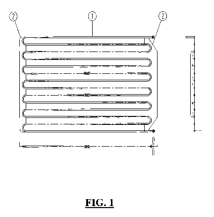
- Figure 1 is a drawing of an individual electrode according to the
invention;
10 - Figure 2 illustrates one embodiment of a multiple electrode arrangement
that can be fitted into a vacuum chamber according to the invention.
Example 1: Electrode placement in the reaction chamber
The arrangement is preferably as shown in Figure 1 and 2. The electrode
arrangement for generating a low pressure plasma comprises a set of floating
electrodes (1) that are hollow, curved and circular in shape, and the vacuum
chamber (5) functions as a mass. The electrodes (1) is fed with a liquid,
which
can be cooled or heated to enable the plasma processes to be performed overin
a
temperature range of 5 to 200 C, and preferably at a controlled temperature
between 20 and 90 C.
A typical electrode (i) in this arrangement has a diameter of between 5 and 50
mm, a wall thickness of 0.25 to 2.5 mm, bending toward the end with a turning
circle of 180 , and the distance between the tube before and after the curve
is
between I and 10 times the pipe diameter, preferably 5 times.
Power is applied to the electrode (1) via connecting plates (2) mounted on a
clutch
plate (4). A thin insulating layer or shield (3) is applied between the clutch
plate
(4) and chamber (5). The thickness of this layer, typically a few millimetres,
is
such that in between no plasma is possible.
CA 02786855 2012-07-11
WO 2011/089009 PCT/EP2011/000242
11
The three-dimensional structure or installation to which the nanocoating is to
be
applied, is positioned between the electrodes, by using a perforated metal
container or tray (6) that can be pushed between the electrodes for example.
It is
preferable that a minimum distance of a few mm is maintained between the
electrode and the substrate. The floating electrodes in the apparatus
described
above enables a uniform three-dimensional coating to be applied in a single
process step. It is not necessary for the top and bottom of a structure to be
coated
in two different steps.
The electrodes generate a high frequency electric field at frequencies between
20
kHz to 2.45 GHz, typically 40 kHz or 13.56 MHz, with 13.56 MHz being
preferred.
Such an electrode arrangement was fitted into a CD 1000 plasma system .
Example 2: Low pressure plasma polymerization of an implanted circuit
board for phone C3F6.
An assembled circuit board for a mobile phone was placed in a CD 1000 plasma
chamber, as described in Example 1, for over two minutes and degassed at a
pressure between 100 and 1000 mTorr. Then the board was cleaned and etched
using Ar, and plasma polymerization was carried out for i0 min using a C3r6
monomer at 50 mTorr and at room temperature. The fluoropolymer conformal
coating applied by this process was measured to be approximately 80 nm thick.
This circuit board was then exposed to several aging processes involving
prolonged exposure to humidity, high temperatures and salt fumes. Visually it
could be seen that the circuit board with the conformal nano coating showed
significantly less corrosion than an untreated circuit board. When carrying
out
electrical testing, it was also found that the circuit board assembly with the
CA 02786855 2012-07-11
WO 2011/089009 PCT/EP2011/000242
12
nanoconformal coating showed virtually no electrical failures, which was
significantly less than the uncoated circuit board assemblies.