Note: Descriptions are shown in the official language in which they were submitted.
CA 02787254 2012-07-16
METHOD AND APPARATUS FOR TRANSMITTING UPLINK CONTROL
INFORMATION IN A WIRELESS COMMUNICATION SYSTEM
BACKGROUND OF THE INVENTION
Field of the Invention
[01] The present invention relates to wireless communications, and more
particularly, to a
method and apparatus for transmitting uplink control information in a wireless
communication system.
Related Art
[02] Effective transmission/reception methods and utilizations have been
proposed for a
broadband wireless communication system to maximize efficiency of radio
resources.
An orthogonal frequency division multiplexing (OFDM) system capable of
reducing
inter-symbol interference (1ST) with a low complexity is taken into
consideration as
one of next generation wireless communication systems. In the OFDM, a serially
input data symbol is converted into N parallel data symbols, and is then
transmitted
by being carried on each of separated N subcarriers. The subcarriers maintain
orthogonality in a frequency dimension. Each orthogonal channel experiences
mutually independent frequency selective fading, and an interval of a
transmitted
symbol is increased, thereby minimizing inter-symbol interference.
[03] When a system uses the OFDM as a modulation scheme, orthogonal
frequency
division multiple access (OFDMA) is a multiple access scheme in which multiple
access is achieved by independently providing some of available subcarriers to
a
plurality of users. In the OFDMA, frequency resources (i.e., subcarriers) are
provided to the respective users, and the respective frequency resources do
not
overlap with one another in general since they are independently provided to
the
plurality of users. Consequently, the frequency resources are allocated to the
respective users in a mutually exclusive manner. In an OFDMA system, frequency
diversity for multiple users can be obtained by using frequency selective
scheduling,
and subcarriers can be allocated variously according to a permutation rule for
the
subcarriers. In addition, a spatial multiplexing scheme using multiple
antennas can
- 1 -
CA 02787254 2012-09-19
53456-59
be used to increase efficiency of a spatial domain.
[04] MIMO technology can be used to improve the efficiency of data
transmission and
reception using multiple transmission antennas and multiple reception
antennas. MIMO
technology may include a space frequency block code (SFBC), a space time block
code
(STBC), a cyclic delay diversity (CDD), a frequency switched transmit
diversity (FSTD), a
time switched transmit diversity (TSTD), a precoding vector switching (PVS),
spatial
multiplexing (SM) for implementing diversity. An MIMO channel matrix according
to the
number of reception antennas and the number of transmission antennas can be
decomposed
into a number of independent channels. Each of the independent channels is
called a layer or
stream. The number of layers is called a rank.
[05] Uplink control information (UCI) can be transmitted through a physical
uplink control
channel (PUCCH). The UCI can include various types of information such as a
scheduling
request (SR), an acknowledgement/non-acknowledgement (ACK/NACK) signal for
hybrid
ARQ (HARQ), a channel quality indicator (CQI), a precoding matrix indicator
(PMI), a rank
indicator (RI), etc. The PUCCH carries various types of control information
according to a
format.
[06] There is a need for a method for effectively transmitting various types
of UCI.
SUMMARY OF THE INVENTION
[07] The present invention provides a method and apparatus for transmitting
uplink control
information in a wireless communication system.
[07a] According to an aspect of the present invention, there is provided a
method for
transmitting uplink control information (UCI) by a user equipment on a
physical uplink
control channel (PUCCH) in a wireless communication system, the method
comprising:
performing channel coding on information bits of the UCI to generate encoding
information
bits, wherein the information bits of the UCI include concatenation of hybrid
automatic repeat
request (IARQ)-ACK(aclulowledgement) information bits for each of serving
cells and a
scheduling request (SR), and wherein the SR is appended at the end of the
concatenated
- 2 -
CA 02787254 2014-11-03
53456-59
HARQ-ACK information bits; scrambling the encoding information bits based on a
user
equipment (UE)-specific scrambling sequence to generate scrambled bits;
modulating the
scrambled bits to generate complex modulation symbols; block-wise spreading
the complex
modulation symbols on the basis of an orthogonal sequence; and transmitting
the block-wise
spread complex modulation symbols to a base station.
[08] In another aspect, a method for transmitting uplink control information
(UCI) by a user
equipment in a wireless communication system is provided. The method includes
performing
channel coding on information bits of the UCI to generate encoding information
bits,
modulating the generated encoding information bits to generate complex
modulation symbols,
block-wise spreading the complex modulation symbols to multiple single carrier-
frequency
division multiple access (SC-FDMA) symbols on the basis of an orthogonal
sequence, and
transmitting the spread complex modulation symbols to a base station.
[09] In some embodiments, information bits of the UCI may include an
information bit of
first UCI and an information bit of second UCI, and channel coding may be
performed by
joint-coding the information bit of the first UCI and the information bit of
the second UCI. In
some embodiments, the information bit of the first UCI may be an
acknowledgement/non-
acknowledgement (ACK/NACK) bit-stream concatenated with an ACK/NACK
information
bit for each of multiple serving cells, and the information bit of the second
UCI may be a
scheduling request (SR). The SR may be added to a last part of the ACK/NACK
bit-stream.
The SR may be one bit. If the SR is 1, it may indicate a presence of an SR
transmission event,
and if the SR is 0, it may indicate an absence of the SR transmission event.
[010] In some embodiments, information bits of the UCI may be information bits
of specific
UCI having a higher priority according to a predetermined priority. The
information bits of
the UCI may be an ACK/NACK signal for multiple component carriers (CCs).
[011] In some embodiments, the information bits of the UCI may include a
representative
ACK/NACK signal which represents respective ACK/NACK information for multiple
CCs.
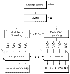
- 3 -
CA 02787254 2014-11-03
53456-59
[012] In some embodiments, the method may further include transmitting an
uplink reference
signal by using at least two SC-FDMA symbols per slot. Phase modulation with -
1 may be
performed on at least one uplink reference signal among uplink reference
signals transmitted
by using the at least two SC-FDMA symbols.
[013] In some embodiments, the method may further include transmitting a
sounding
reference signal (SRS) by using at least one SC-FDMA symbol per subframe. A
length of the
orthogonal code may be determined based on the number of SC-FDMA symbols for
transmitting the SRS.
[014] In some embodiments, the orthogonal code may be any one of a Walsh code
or a
discrete Fourier transform (DFT) code.
[014a] According to another aspect of the present invention, there is provided
a user
equipment comprising: a radio frequency (RF) unit for transmitting or
receiving a radio
signal; and a processor coupled to the RF unit, wherein the processor is
configured for:
performing channel coding on information bits of uplink control information
(UCI) to
generate encoding information bits, wherein the information bits of the UCI
include
concatenation of hybrid automatic repeat request (HARQ)-ACK(acknowledgement)
information bits for each of serving cells and a scheduling request (SR), and
wherein the SR is
appended at the end of the concatenated HARQ-ACK information bits; scrambling
the
encoding information bits based on a user equipment (UE)-specific scrambling
sequence to
generate scrambled bits; modulating the scrambled bits to generate complex
modulation
symbols; block-wise spreading the complex modulation symbols on the basis of
an orthogonal
sequence; and transmitting the block-wise spread complex modulation symbols to
a base station.
[015] In another aspect, a user equipment is provided. The user equipment
includes a radio
frequency (RF) unit for transmitting or receiving a radio signal, and a
processor coupled to the
RF unit, wherein the processor is configured for performing channel coding on
information
bits of uplink control information (UCI) to generate encoding information
bits, modulating the
generated encoding information bits to generate complex modulation symbols,
and block-wise
spreading the complex modulation symbols to multiple single carrier-frequency
division
multiple access (SC-FDMA) symbols on the basis of an orthogonal sequence.
- 3a -
CA 02787254 2012-07-16
[016] Various types of uplink control information (UCI) can be effectively
transmitted
without collision when the UCI needs to be transmitted in the same subframe or
the
same slot.
BRIEF DESCRIPTION OF THE DRAWINGS
[017] FIG. 1 shows a wireless communication system.
[018] FIG. 2 shows the structure of a radio frame in 3GPP LTE.
[019] FIG. 3 shows an example of a resource grid of a single downlink slot.
[020] FIG. 4 shows the structure of a downlink subframe.
[021] FIG. 5 shows the structure of an uplink subframe.
[022] FIG. 6 shows a PUCCH format la/lb in a normal CP structure.
[023] FIG. 7 shows a PUCCH format la/lb in an extended CP structure.
[024] FIG. 8 shows a PUCCH format 2/2a/2b.
[025] FIG. 9 shows an example of the structure of a transmitter in an SC-FDMA
system.
[026] FIG. 10 shows an example of a scheme in which the subcarrier mapper maps
the
complex-valued symbols to the respective subcarriers of the frequency domain.
[027] FIG. 11 to FIG. 13 show example of a transmitter using the clustered DFT-
s OFDM
transmission scheme.
[028] FIG. 14 to FIG. 16 show an example of a transmitter and a receiver which
constitute
a carrier aggregation system.
[029] FIG. 17 is a block diagram of a case where 5 downlink component carriers
(DL CCs)
correspond to one uplink component carrier (UL CC) in a carrier aggregation
system.
[030] FIG. 18 and FIG. 19 are example of an extended PUCCH format.
[031] FIG. 20 and FIG. 21 show example of time spreading for a modulated QPSK
symbol
with an extended PUCCH format.
[032] FIG. 22 and FIG. 23 are another example of an extended PUCCH format.
[033] FIG. 24 is an example of a case where a UE transmits ACKNACK and SR.
[034] FIG. 25 is an example of configuring ACK/NACK bundling according to the
proposed UCI transmission method.
[035] FIG. 26 shows an example of a case where phase modulation is performed
according
to the proposed UCI transmission method.
- 4 -
,
CA 02787254 2012-07-16
,
[036] FIG. 27 to FIG. 30 are another example of an extended PUCCH format.
[037] FIG. 31 to FIG. 33 show example of a subframe configuration according to
the
proposed UCI transmission method.
[038] FIG. 34 is another example of an extended PUCCH format.
[039] FIG. 35 is a block diagram showing a BS and a UE according to an
embodiment of
the present invention.
DESCRIPTION OF EXEMPLARY EMBODIMENTS
[040] The following technique may be used for various wireless communication
systems
such as code division multiple access (CDMA), a frequency division multiple
access
(FDMA), time division multiple access (TDMA), orthogonal frequency division
_
multiple access (OFDMA), single carrier-frequency division multiple access (SC-
FDMA), and the like. The CDMA may be implemented as a radio technology such
as universal terrestrial radio access (UTRA) or CDMA2000. The TDMA may be
implemented as a radio technology such as a global system for mobile
communications (GSM)/general packet radio service (GPRS)/enhanced data rates
for
GSM evolution (EDGE). The OFDMA may be implemented by a radio technology
such as institute of electrical and electronics engineers (IEEE) 802.11 (Wi-
Fi), IEEE
802.16 (WiMAX), IEEE 802.20, E-UTRA (evolved UTRA), and the like. IEEE
802.16m, an evolution of IEEE 802.16e, provides backward compatibility with a
system based on IEEE 802.16e. The UTRA is part of a universal mobile
telecommunications system (UMTS). 3GPP (3rd generation partnership project)
LTE (long term evolution) is part of an evolved UMTS (E-UMTS) using the E-
UTRA, which employs the OFDMA in downlink and the SC-FDMA in uplink.
LIE-A (advanced) is an evolution of 3GPP LIE.
[041] Hereinafter, for clarification, LIE-A will be largely described, but the
technical
concept of the present invention is not meant to be limited thereto.
[042] FIG. 1 shows a wireless communication system.
[043] The wireless communication system 10 includes at least one base station
(BS) 11.
Respective BSs 11 provide a communication service to particular geographical
areas
15a, 15b, and 15c (which are generally called cells). Each cell may be divided
into
- 5 -
,
CA 02787254 2012-07-16
,
a plurality of areas (which are called sectors). A user equipment (UE) 12 may
be
fixed or mobile and may be referred to by other names such as MS (mobile
station),
MT (mobile terminal), UT (user terminal), SS (subscriber station), wireless
device,
PDA (personal digital assistant), wireless modem, handheld device. The BS 11
generally refers to a fixed station that communicates with the UE 12 and may
be
called by other names such as eNB (evolved-NodeB), BTS (base transceiver
system),
access point (AP), etc.
[044] In general, a UE belongs to one cell, and the cell to which a UE belongs
is called a
serving cell. A BS providing a communication service to the serving cell is
called a
serving BS. The wireless communication system is a cellular system, so a
different
cell adjacent to the serving cell exists. The different cell adjacent to the
serving cell
is called a neighbor cell. A BS providing a communication service to the
neighbor
cell is called a neighbor BS. The serving cell and the neighbor cell are
relatively
determined based on a UE.
[045] This technique can be used for downlink or uplink. In general, downlink
refers to
communication from the BS 11 to the UE 12, and uplink refers to communication
from the UE 12 to the BS 11. In downlink, a transmitter may be part of the BS
11
and a receiver may be part of the UE 12. In uplink, a transmitter may be part
of the
UE 12 and a receiver may be part of the BS 11.
[046] The wireless communication system may be any one of a multiple-input
multiple-
output (MIMO) system, a multiple-input single-output (MISO) system, a single-
input
single-output (SISO) system, and a single-input multiple-output (SIMO) system.
The MIMO system uses a plurality of transmission antennas and a plurality of
reception antennas. The MISO system uses a plurality of transmission antennas
and
a single reception antenna. The SISO system uses a single transmission antenna
and a single reception antenna. The SIMO system uses a single transmission
antenna and a plurality of reception antennas. Hereinafter, a transmission
antenna
refers to a physical or logical antenna used for transmitting a signal or a
stream, and a
reception antenna refers to a physical or logical antenna used for receiving a
signal or
a stream.
[047] FIG. 2 shows the structure of a radio frame in 3GPP LTE.
[048] It may be referred to Paragraph 5 of "Technical Specification Group
Radio Access
- 6 -
, CA 02787254 2012-07-16
Network; Evolved Universal Terrestrial Radio Access (E-UTRA); Physical
channels
and modulation (Release 8)" to 3GPP (3rd generation partnership project) TS
36.211
V8.2.0 (2008-03). Referring to FIG. 2, the radio frame includes 10 subframes,
and
one subframe includes two slots. The slots in the radio frame are numbered by
#0
to #19. A time taken for transmitting one subframe is called a transmission
time
interval (TTI). The TTI may be a scheduling unit for a data transmission. For
example, a radio frame may have a length of 10 ms, a subframe may have a
length of
1 ms, and a slot may have a length of 0.5 ms.
[049] One slot includes a plurality of orthogonal frequency division
multiplexing (OFDM)
symbols in a time domain and a plurality of subcarriers in a frequency domain.
_
Since 3GPP LTE uses OFDMA in downlink, the OFDM symbols are used to express
a symbol period. The OFDM symbols may be called by other names depending on a
..
multiple-access scheme. For example, when a single carrier frequency division
multiple access (SC-FDMA) is in use as an uplink multi-access scheme, the OFDM
symbols may be called SC-FDMA symbols. A resource block (RB), a resource
allocation unit, includes a plurality of continuous subcarriers in a slot. The
structure
of the radio frame is merely an example. Namely, the number of subframes
included in a radio frame, the number of slots included in a subframe, or the
number
of OFDM symbols included in a slot may vary.
[050] 3GPP LTE defines that one slot includes seven OFDM symbols in a normal
cyclic
prefix (CP) and one slot includes six OFDM symbols in an extended CP.
[051] The wireless communication system may be divided into a frequency
division duplex
(FDD) scheme and a time division duplex (TDD) scheme. According to the FDD
scheme, an uplink transmission and a downlink transmission are made at
different
frequency bands. According to the TDD scheme, an uplink transmission and a
downlink transmission are made during different periods of time at the same
frequency band. A channel response of the TDD scheme is substantially
reciprocal.
This means that a downlink channel response and an uplink channel response are
almost the same in a given frequency band. Thus, the TDD-based wireless
communication system is advantageous in that the downlink channel response can
be
obtained from the uplink channel response. In the TDD scheme, the entire
frequency band is time-divided for uplink and downlink transmissions, so a
downlink
- 7 -
,
CA 02787254 2012-07-16
transmission by the BS and an uplink transmission by the UE can be
simultaneously
performed. In a TDD system in which an uplink transmission and a downlink
transmission are discriminated in units of subframes, the uplink transmission
and the
downlink transmission are performed in different subframes.
[052] FIG. 3 shows an example of a resource grid of a single downlink slot.
[053] A downlink slot includes a plurality of OFDM symbols in the time domain
and NRB
number of resource blocks (RBs) in the frequency domain. The NRB number of
resource blocks included in the downlink slot is dependent upon a downlink
transmission bandwidth set in a cell. For example, in an LTE system, NRB may
be
any one of 60 to 110. One resource block includes a plurality of subcarriers
in the
frequency domain. An uplink slot may have the same structure as that of the
downlink slot.
[054] Each element on the resource grid is called a resource element. The
resource
elements on the resource grid can be discriminated by a pair of indexes (k,l)
in the
slot. Here, k (k=0,...,NRBx12-1) is a subcarrier index in the frequency
domain, and I
is an OFDM symbol index in the time domain.
[055] Here, it is illustrated that one resource block includes 7x12 resource
elements made
up of seven OFDM symbols in the time domain and twelve subcarriers in the
frequency domain, but the number of OFDM symbols and the number of subcarriers
in the resource block are not limited thereto. The number of OFDM symbols and
the number of subcarriers may vary depending on the length of a cyclic prefix
(CP),
frequency spacing, and the like. For example, in case of a normal CP, the
number
of OFDM symbols is 7, and in case of an extended CP, the number of OFDM
symbols is 6. One of 128, 256, 512, 1024, 1536, and 2048 may be selectively
used
as the number of subcarriers in one OFDM symbol.
[056] FIG. 4 shows the structure of a downlink subframe.
[057] A downlink subframe includes two slots in the time domain, and each of
the slots
includes seven OFDM symbols in the normal CP. First three OFDM symbols
(maximum four OFDM symbols with respect to a 1.4 MHz bandwidth) of a first
slot
in the subframe corresponds to a control region to which control channels are
allocated, and the other remaining OFDM symbols correspond to a data region to
which a physical downlink shared channel (PDSCH) is allocated.
- 8 -
CA 02787254 2012-07-16
[058] The PDCCH may carry a transmission format and a resource allocation of a
downlink shared channel (DL-SCH), resource allocation information of an uplink
shared channel (UL-SCH), paging information on a PCH, system information on a
DL-SCH, a resource allocation of an higher layer control message such as a
random
access response transmitted via a PDSCH, a set of transmission power control
commands with respect to individual UEs in a certain UE group, an activation
of a
voice over interne protocol (VoIP), and the like. A plurality of PDCCHs may be
transmitted in the control region, and a UE can monitor a plurality of PDCCHs.
The PDCCHs are transmitted on one or an aggregation of a plurality of
consecutive
control channel elements (CCE). The CCE is a logical allocation unit used to
provide a coding rate according to the state of a wireless channel. The CCE
corresponds to a plurality of resource element groups. The format of the PDCCH
and an available number of bits of the PDCCH are determined according to an
associative relation between the number of the CCEs and a coding rate provided
by
the CCEs.
[059] The BS determines a PDCCH format according to a DCI to be transmitted to
the UE,
and attaches a cyclic redundancy check (CRC) to the DCI. A unique radio
network
temporary identifier (RNTI) is masked on the CRC according to the owner or the
purpose of the PDCCH. I n case of a PDCCH for a particular UE, a unique
identifier, e.g., a cell-RNTI (C-RNTI), of the UE, may be masked on the CRC.
Or,
in case of a PDCCH for a paging message, a paging indication identifier, e.g.,
a
paging-RNTI (P-RNTI), may be masked on the CRC. In case of a PDCCH for a
system information block (SIB), a system information identifier, e.g., a
system
information-RNTI (SI-RNTI), may be masked on the CRC. In order to indicate a
random access response, i.e., a response to a transmission of a random access
preamble of the UE, a random access-RNTI (RA-RNTI) may be masked on the CRC.
[060] FIG. 5 shows the structure of an uplink subframe.
[061] An uplink subframe may be divided into a control region and a data
region in the
frequency domain. A physical uplink control channel (PUCCH) for transmitting
uplink control information is allocated to the control region. A physical
uplink
shared channel (PUCCH) for transmitting data is allocated to the data region.
I f
indicated by a higher layer, the user equipment may support simultaneous
- 9 -
CA 02787254 2012-07-16
transmission of the PUCCH and the PUSCH.
[062] The PUSCH is mapped to a uplink shared channel (UL-SCH), a transport
channel.
Uplink data transmitted on the PUSCH may be a transport block, a data block
for the
UL-SCH transmitted during the TTI. The transport block may be user
information.
Or, the uplink data may be multiplexed data. The multiplexed data may be data
obtained by multiplexing the transport block for the UL-SCH and control
information. For example, control information multiplexed to data may include
a
CQI, a precoding matrix indicator (PMI), an HARQ, a rank indicator (RI), or
the like.
Or the uplink data may include only control information.
[063] The following description is about a PUCCH.
[064] The PUCCH for one UE is allocated in an RB pair. RBs belonging to the RB
pair
occupy different subcarriers in each of a 1st slot and a 2nd slot. A frequency
occupied by the RBs belonging to the RB pair allocated to the PUCCH changes at
a
slot boundary. This is called that the RB pair allocated to the PUCCH is
frequency-
hopped at a slot boundary. Since the TIE transmits UL control information over
time through different subcarriers, a frequency diversity gain can be
obtained. In
the figure, m is a location index indicating a logical frequency-domain
location of the
RB pair allocated to the PUCCH in the subframe.
[065] The PUCCH carries various types of control information according to a
format. A
PUCCH format 1 carries a scheduling request (SR). In this case, an on-off
keying
(00K) scheme can be used. A PUCCH format la carries an
acknowledgement/non-acknowledgement (ACK/NACK) modulated by using bit
phase shift keying (BPSK) with respect to one codeword. A PUCCH format lb
carries an ACK/NACK modulated by using quadrature phase shift keying (QPSK)
with respect to two codewords. A PUCCH format 2 carries a channel quality
indicator (CQI) modulated by using QPSK. PUCCH formats 2a and 2b carry CQI
and ACK/NACK.
[066] Table 1 shows a modulation scheme and the number of bits in a subframe
according
to a PUCCH format.
[067] [Table 1]
- 10 -
CA 02787254 2012-07-16
PUCCH format Modulation scheme Number of bits per subframe, Mbit
1 N/A N/A
1 a BPSK 1
lb QPSK 2
2 QPSK 20
2a QPSK+BPSK 21
2b QPSK+QPSK 22
[068] Table 2 shows the number of OFDM symbols used as a PUCCH demodulation
reference signal per slot.
[069] [Table 2]
PUCCH format Normal cyclic prefix Extended cyclic prefix
1, la, lb 3 2
2 2 1
2a, 2b 2 N/A
[070] Table 3 shows a position of an OFDM symbol to which a demodulation
reference
signal is mapped according to a PUCCH format.
[071] [Table 3]
PUCCH format set of values for C
Normal cyclic prefix Extended cyclic prefix
1,1a, lb 2, 3, 4 2,3
2, 2a, 2b 1,5 3
[072] ACK/NACK signals can be transmitted by using different resources
including
different cyclic shift values and different Walsh/discrete Fourier transform
(DFT)
orthogonal codes by using a computer generated constant amplitude zero auto
correlation (CG-CAZAC) sequence for each UE. If an available cyclic shift
value
is 6 and the number of Walsh/DFT codes is 3, 18 UEs having a signal antenna
port
can be multiplexed in one PRB.
[073] FIG. 6 shows a PUCCH format la/lb in a normal CP structure. Uplink
reference
signals are transmitted in 3rd to 5th SC-FDMA symbols. In FIG. 6, WO, wt, wz
and
w3 can be modulated in a time domain after inverse fast Fourier transform
(IFFT)
modulation, or can be modulated in a frequency domain before IFFT modulation.
[074] FIG. 7 shows a PUCCH format la/lb in an extended CP structure. Uplink
reference signals are transmitted in 3rd and 4th SC-FDMA symbols. In FIG. 7,
wo,
vsi2 and w3 can be modulated in a time domain after IFFT modulation, or can be
modulated in a frequency domain before IFFT modulation.
[075] An ACK/NACK resource including an SR, a cyclic shift assigned to the UE
for
persistent scheduling, a Walsh/DFT code, a PRB, or the like can be given by
using
RRC signaling. For non-persistent scheduling for dynamic ACK/NACK, the
- 11 ¨
CA 02787254 2012-07-16
allocated resource can be given by a lowest CCE index of a PDCCH corresponding
to a PDSCH for the ACK/NACK.
[076] Table 4 is an example of an orthogonal sequence with a length of 4 for
the PUCCH
format 1/1a/lb.
[077] [Table 4]
Sequence index n0(n5) Orthogonal sequences [w(0)
w(,/sFpuccu.1)1
0 [+1 +1 +1 +1]
1 [+1 -1 +1 -1]
2 [+1 -1 -1 +1]
[078] Table 5 is an example of an orthogonal sequence with a length of 3 for
the PUCCH
format 1/1a/lb.
= [079] [Table 5]
Sequence index n0(n5) Orthogonal sequences [w(0) w(NsFPuccH-1)]
0 [1 1 1]
1 [1 &It/3 ei4rt/3]
2 [1 ep4iii3 ej27L13]
[080] Table 6 is an example of an orthogonal sequence for reference signal
transmission in
the PUCCH format 1/1a/lb.
[081] [Table 6]
Sequence index noc2(ns) Normal cyclic prefix Extended cyclic
prefix
0 [1 1 1] [11]
1 [1 e23 ej4it/3] [1 -1]
2 [1 ei4n/3 &Zan] N/A
[082] Table 7 is an example of ACKNACK channelization when AshiftpuccH=2 in a
normal
CP structure.
[083] [Table 7]
Cell specific cyclic shift RS orthogonal cover ACKNACK orthogonal
cover
offset
6.ffsetPUCCH= 6offsetpuccii=1) floc 7 =0 floc '= 1 noc'=2
noc=0 noc=1 noc=2
ncs=1 ncs=0 n'=0 12 n'=0 12
2 1 6 6
3 2 1 13 1 13
4 3 7 7
5 4 2 14 2 14
6 5 8 8
7 6 3 15 3 15
8 7 9 9
9 8 4 16 4 16
10 9 10 10
11 10 5 17 5 17
0 11 11 11
[084] In Table 7, AshiftPLCCH is a cell-specific cyclic shift value of a CAZAC
sequence, and
may have any one of values 1 to 3 in a normal CP structure or an extended CP
¨ 12 ¨
CA 02787254 2012-07-16
structure. ooffsetpucal .s
a cell-specific cyclic shift offset, and may have any one of
values 0 to Ash,ftPucCH-1. Meanwhile, noc is an index of an orthogonal
sequence for
ACK/NACK, and floc' is an index of an orthogonal sequence for a reference
signal.
ncs is a cyclic shift value of a CAZAC sequence, and n' is an ACK/NACK
resource
index used for channelization in an RB.
[085] Table 8 is an example of channelization of a structure in which a PUCCH
format
1/1a/lb and a PUCCH format 2/2a/2b are mixed in a PRB.
[086] [Table 8]
Orthogonal cover
Cyclic Shift OCindex=0 OCindex-1 OCindex=2
0 ACK/NACK
1 ACK/NACK
2 ACK/NACK
3 ACK/NACK
4 Guard shifts
5 CQI
6 CQI
7 CQI
8 CQI
9 CQI
CQI
11 Guard shifts
[087] Referring to Table 8, cyclic shift values 0 to 3 for the PUCCH format
1/1a/lb are
10 allocated, and cyclic shift values 5 to 10 for the PUCCH format 2/2a/2b
are allocated.
Cyclic shift values 4 and 11 between the PUCCH format 1/1a/lb and the PUCCH
format 2/2a/2b are allocated as a guard shift.
[088] Meanwhile, cyclic shift hopping can be performed on a symbol basis for
inter-cell
interference (ICI) randomization. In addition, for the ICI randomization,
CS/orthogonal covering (OC) remapping can be performed between an ACK/NACK
channel and a resource in a slot level.
[089] A resource for the PUCCH format 1/1a/lb can consist of rk, indicating a
cyclic shift
in a symbol level, noc indicating orthogonal covering in a slot level, and nRB
indicating a resource block in a frequency domain. nr can be defined as an
index
representing the PUCCH format 1/1a/lb resources ncs, n.c, nR13. That is,
nr----(nes,noonRa)=
[090] The PUCCH format 2/2a/2b can carry control information such as a CQI, a
precoding matrix indicator (PMI), a rank indicator (RI), CQI+ACK/NACK, etc. A
Reed-Muller (RM) channel coding scheme can be applied to the PUCCH format
- 13 -
CA 02787254 2012-07-16
2/2a/2b.
[091] Table 9 shows an example of a (20,A) RM code used in channel coding of
uplink
control information (UCI) of 3GPP LTE. A bit-stream ao,alia2,...,aA..1 is used
as an
input of a channel coding block using the (20,A) RM code of Table 9.
[092] [Table 9]
i M10 Mi,1 M1,2 Mi,3 Mi,4 M1,5 M1,6 M1,7 Mi,8 Mi,9 M1,10 M1,11
M1,12
0 1 1 0 0 0 -0 0 0 0 0 1 1 p
1 1 1 1 0 0 0 ,0 0 0 1 1 1 0
2 1 0 0 1 0 0 1 0 1 1 1 1 1
3 1 0 1 1 0 0 0 0 1 0 1 1 1
4 1 1 1 1 0 0 0 1 0 0 1 1 1
5 1 1 0 0 1 0 1 ,1 1 0 1 1 1
6 1 0 1 0 1 0 1 0 1 I 1 1 1
7 1 0 0 1 1 0 0 I 1 0 1 1 1
8 1 1 0 1 1 0 0 1 0 1 1 1 1
9 1 0 1 1 1 0 1 0 0 1 1 1 1
1 0 1 0 0 1 1 ,1 0 1 1 1 1
11 I 1 1 0 0 1 ,1 0 1 0 1 1 1
12 1 0 0 1 0 1 0 1 1 1 1 1 ,1
13 1 1 0 1 0 1 0 1 0 1 1 1 1
14 1 0 0 0 1 1 0 1 0 0 1 0 1
1 1 0 0 1 1 1 1 0 1 1 0 1
16 1 1 1 0 1 1 1 0 0 1 0 1 I
17 1 0 0 1 1 1 0 0 1 0 0 1 ,1
18 1 1 ,0 1 1 1 1 1 0 0 0 0 0
19 1 0 0 0 0 1 1 0 0 0 0 0 0
[093] Channel encoding bits bo,bi,b2,...,bB_I can be generated by Equation 1
below.
[094] <Equation 1>
A-1
= l(an = Mi,) mod 2
[095] n=0
[096] In Equation 1,
10 [097] Table 10 shows an example of a size of a CQI feedback UCI field
for wideband
reporting. Table 11 is a case where a single-antenna port is assumed, and
transmit
diversity or open-loop spatial multiplexing PDSCH transmission is assumed.
[098] [Table 101
Field Bitwidth
Wide-band CQI 4
[099] Table 11 is an example of a CQI and PMI feedback UCI field for wideband
reporting.
15 Table 11 is a case of closed-loop spatial multiplexing PDSCH
transmission.
- 14 -
CA 02787254 2012-07-16
[0100] [Table 11]
Bitwidths
Field 2 antenna ports 4 antenna ports
Rank = 1 Rank = 2 Rank = I Rank > I
Wide-band CQI 4 4 4 4
Spatial differential CQI 0 3 0 3
Precoding matrix indication 2 1 4 4
[0101] Table 12 is an example of a size of an RI feedback UCI field for
wideband reporting.
[0102] [Table 12]
Bitwidths
Field 4 antenna ports
2 antenna ports
Max 2 layers Max 4 layers
=
Rank indication 1 1 2
[0103] In this case, ao and aA_I respectively denote a most significant bit
(MSB) and a least
significant bit (LSB). In the extended CP structure, A can be up to 11 except
for a
case where CQI and ACK/NACK are simultaneously transmitted. QPSK
modulation can be applied to control information encoded into 20 bits by using
an
RM code. In addition, the encoded control information can be scrambled before
QPSK modulation.
[0104] FIG. 8 shows a PUCCH format 2/2a/2b. FIG. 8(a) shows a normal CP
structure,
and FIG. 8(b) shows an extended CP structure. In FIG. 8(a), reference signals
are
transmitted in ri and 6th SC-FDMA symbols. In FIG. 8(b), reference signals are
transmitted in a 4th SC-FDMA symbol.
[0105] In a normal CP structure, one subframe includes 10 QPSK data symbols
except for
an SC-FDMA symbol for reference signal transmission. That is, each QPSK
symbol can be spread by a cyclic shift in an SC-FDMA symbol level by using a
20-
bit encoded CQI.
[0106] In addition, SC-FDMA symbol level cyclic shift hopping can be applied
for ICI
randomization. A reference signal can be multiplexed according to code
division
multiplexing (CDM) by using a cyclic shift. For example, if the number of
available cyclic shift values is 12, 12 UEs can be multiplexed in one PRB.
That is,
each of a plurality of UEs in a PUCCH format 1/1a/lb and a PUCCH format
2/2a/2b
can be multiplexed by using a cyclic shift/orthogonal covering/resource block
and a
cyclic shift/resource block.
[0107] A PRB used for PUCCH transmission in a slot ns can be determined by
Equation 2.
[0108] <Equation 2>
- 15 -
'
, CA 02787254 2012-07-16
if (m + ns mod 2) mod 2 = 0
L I 2 J
_
nPRB ¨ lin 1
UL
N RB ¨1 _[¨nij if (m + ns mod 2) mod 2 =1
[0109] 2
[0110] In Equation 2, ElpRB denotes a PRB index. NRBul- is an uplink bandwidth
configuration expressed with a multiple of NscRB. NscRB is a size of a
resource
block in a frequency domain and is expressed with the number of subcarriers.
When the PRB is mapped to a PRB, the PUCCH can be mapped in the order of an
outer PRB and an inner PRB. In addition, it can be mapped in the order of a
- PUCCH format 2/2a/2b, an ACK/NACK combination format, and a
PUCCH format
1/1a/lb.
..
[0111] In the PUCCH format 1/1a/lb, m can be determined by Equation 3.
[0112] <Equation 3>
' N2 if ng)JCCH < C.
NCs1)/ A sPa hift
CH
m= , n(1) [ _ c . N(1) / A (1)
PIXCH
PUCCH
C = NRB cs shift
NM 4_ otherwise
A/ PUCCH RB 8
sc ' shift N cs
, _
C = 3 normal cyclic prefix
[0113] 2 extended cyclic prefix
[0114] In Equation 3, N1B(2) denotes a bandwidth expressed with a resource
block that can
be used in the PUCCH format 2/2a/2b in each slot. npucciP) denotes an index of
a
resource used for PUCCH format 1/1a/lb transmission. N2) denotes the number
of cyclic shift values used for the PUCCH format 1/1a/lb in a resource block
used in
a mixed structure of the PUCCH format 1/la/lb and format 2/2a/2b.
[0115] In the PUCCH format 2/2a/2b, m can be determined by Equation 4.
[0116] <Equation 4>
RB
M =Ln2)
(
PUCCH /N]
[0117]
[0118] In an LTE-A system, UL adopts an SC-FDMA transmission scheme. A
transmission scheme in which IFFT is performed after DFT spreading is called
SC-
FDMA. SC-FDMA may also be called a discrete Fourier transform spread (DFT-s)
OFDM. In SC-FDMA, the peak-to-average power ratio (PAPR) or a cubic metric
(CM) may be lowered. If the SC-FDMA transmission scheme is used, transmission
- 16 -
CA 02787254 2012-07-16
power efficiency in a UE having limited power consumption may be increased
because the non-linear distortion period of a power amplifier may be avoided.
Consequently, user throughput may be increased.
[0119] FIG. 9 shows an example of the structure of a transmitter in an SC-FDMA
system.
[0120] Referring to FIG. 9, the transmitter 50 includes a discrete Fourier
transform (DFT)
unit 51, a subcarrier mapper 52, an inverse fast Fourier transform (IFFT) unit
53, and
a cyclic prefix (CP) insertion unit 54. The transmitter 50 may include a
scramble
unit (not shown), a modulation mapper (not shown), a layer mapper (not shown),
and
a layer permutator (not shown), which may be placed in front of the DFT unit
51.
[0121] The DFT unit 51 outputs complex-valued symbols by performing DFT on
input
symbols. For example, when Ntx symbols are input (where Ntx is a natural
number), a DFT size is Ntx. The DFT unit 51 may be called a transform
precoder.
The subcarrier mapper 52 maps the complex-valued symbols to the respective
subcarriers of the frequency domain. The complex-valued symbols may be mapped
to resource elements corresponding to a resource block allocated for data
transmission. The subcarrier mapper 52 may be called a resource element
mapper.
The IFFT unit 53 outputs a baseband signal for data (that is, a time domain
signal) by
performing IFFT on the input symbols. The CP insertion unit 54 copies some of
the
rear part of the baseband signal for data and inserts the copied parts into
the former
part of the baseband signal for data. Orthogonality may be maintained even in
a
multi-path channel because inter-symbol interference (1ST) and inter-carrier
interference (ICI) are prevented through CP insertion.
[0122] FIG. 10 shows an example of a scheme in which the subcarrier mapper
maps the
complex-valued symbols to the respective subcarriers of the frequency domain.
[0123] Referring to FIG. 10(a), the subcarrier mapper maps the complex-valued
symbols,
outputted from the DFT unit, to subcarriers contiguous to each other in the
frequency
domain. '0' is inserted into subcarriers to which the complex-valued symbols
are
not mapped. This is called localized mapping. In a 3GPP LTE system, a
localized
mapping scheme is used. Referring to FIG. 10(b), the subcarrier mapper inserts
an
(L-1) number of '0' every two contiguous complex-valued symbols which are
outputted from the DFT unit (L is a natural number). That is, the complex-
valued
symbols outputted from the DFT unit are mapped to subcarriers distributed at
equal
- 17 -
CA 02787254 2012-07-16
intervals in the frequency domain. This is called distributed mapping. If the
subcarrier mapper uses the localized mapping scheme as in FIG. 10(a) or the
distributed mapping scheme as in FIG. 10(b), a single carrier characteristic
is
maintained.
[0124] A clustered DFT-s OFDM transmission scheme is a modification of the
existing SC-
FDMA transmission scheme and is a method of dividing data symbols, subjected
to a
precoder, into a plurality of subblocks, separating the subblocks, and mapping
the
subblocks in the frequency domain.
[0125] FIG. 11 shows an example of a transmitter using the clustered DFT-s
OFDM
transmission scheme.
[0126] Referring to FIG. 11, the transmitter 70 includes a DFT unit 71, a
subcarrier mapper
72, an IFFT unit 73, and a CP insertion unit 74. The transmitter 70 may
further
include a scramble unit (not shown), a modulation mapper (not shown), a layer
mapper (not shown), and a layer permutator (not shown), which may be placed in
front of the DFT unit 71.
[0127] Complex-valued symbols outputted from the DFT unit 71 are divided into
N
subblocks (N is a natural number). The N subblocks may be represented by a
subblock #1, a subblock #2, ..., a subblock #N. The subcarrier mapper 72
distributes the N subblocks in the frequency domain and maps the N subblocks
to
subcarriers. The NULL may be inserted every two contiguous subblocks. The
complex-valued symbols within one subblock may be mapped to subcarriers
contiguous to each other in the frequency domain. That is, the localized
mapping
scheme may be used within one subblock.
[0128] The transmitter 70 of FIG. 11 may be used both in a single carrier
transmitter or a
multi-carrier transmitter. If the transmitter 70 is used in the single carrier
transmitter, all the N subblocks correspond to one carrier. If the transmitter
70 is
used in the multi-carrier transmitter, each of the N subblocks may correspond
to one
carrier. Alternatively, even if the transmitter 70 is used in the multi-
carrier
transmitter, a plurality of subblocks of the N subblocks may correspond to one
carrier.
Meanwhile, in the transmitter 70 of FIG. 10, a time domain signal is generated
through one IFFT unit 73. Accordingly, in order for the transmitter 70 of FIG.
10 to
be used in a multi-carrier transmitter, subcarrier intervals between
contiguous
- 18 -
CA 02787254 2012-07-16
carriers in a contiguous carrier allocation situation must be aligned.
[0129] FIG. 12 shows another example of a transmitter using the clustered DFT-
s OFDM
transmission scheme.
[0130] Referring to FIG. 12, the transmitter 80 includes a DFT unit 81, a
subcarrier mapper
82, a plurality of IFFT units 83-1, 83-2, ...,83-N (N is a natural number),
and a CP
insertion unit 84. The transmitter 80 may further include a scramble unit (not
shown), a modulation mapper (not shown), a layer mapper (not shown), and a
layer
permutator (not shown), which may be placed in front of the DFT unit 71.
[0131] IFFT is individually performed on each of N subblocks. An nth IFFT unit
83-n
outputs an nth baseband signal (n=1, 2, ..,N) by performing IFFT on a subblock
#n.
The nth baseband signal is multiplied by an nth carrier signal to produce an
nth radio
signal. After the N radio signals generated from the N subblocks are added, a
CP is
inserted by the CP insertion unit 84. The transmitter 80 of FIG. 12 may be
used in a
discontinuous carrier allocation situation where carriers allocated to the
transmitter
are not contiguous to each other.
[0132] FIG. 13 is another example of a transmitter using the clustered DFT-s
OFDM
transmission scheme.
[0133] FIG. 13 is a chunk-specific DFT-s OFDM system performing DFT precoding
on a
chunk basis. This may be called Nx SC-FDMA. Referring to FIG. 13, the
transmitter 90 includes a code block division unit 91, a chunk division unit
92, a
plurality of channel coding units 93-1, ..., 93-N, a plurality of modulators
94-1, ...,
94-N, a plurality of DFT units 95-1, ..., 95-N, a plurality of subcarrier
mappers 96-
1, ..., 96-N, a plurality of IFFT units 97-1, ..., 97-N, and a CP insertion
unit 98.
Here, N may be the number of multiple carriers used by a multi-carrier
transmitter.
Each of the channel coding units 93-1, ..., 93-N may include a scramble unit
(not
shown). The modulators 94-1, ..., 94-N may also be called modulation mappers.
The transmitter 90 may further include a layer mapper (not shown) and a layer
permutator (not shown) which may be placed in front of the DFT units 95-1,
..., 95-N.
[0134] The code block division unit 91 divides a transmission block into a
plurality of code
blocks. The chunk division unit 92 divides the code blocks into a plurality of
chunks. Here, the code block may be data transmitted by a multi-carrier
transmitter,
and the chunk may be a data piece transmitted through one of multiple
carriers. The
- 19 -
CA 02787254 2014-11-03
53456-59
transmitter 90 performs DFT on a chunk basis. The transmitter 90 may be used
in a
discontinuous carrier allocation situation or a contiguous carrier allocation
situation.
[0135] Meanwhile, a 3GPP LTE-A system supports a carrier aggregation system.
3GPP
TR 36.815 V9Ø0 (2010-3) may be referred to to describe the
carrier aggregation system.
[0136] The carrier aggregation system implies a system that configures a
wideband by
aggregating one or more carriers having a bandwidth smaller than that of a
target
wideband when the wireless communication system intends to support the
wideband.
The carrier aggregation system can also be referred to as other terms such as
a
multiple carrier system, a bandwidth aggregation system, or the like. The
carrier
aggregation system can be divided into a contiguous carrier aggregation system
in
which carriers are contiguous to each other and a non-contiguous carrier
aggregation
system in which carriers are separated from each other. In the contiguous
carrier
aggregation system, a guard band may exist between carriers. A carrier which
is a
target when aggregating one or more carriers can directly use a bandwidth that
is
used in the legacy system in order to provide backward compatibility with the
legacy
system. For example, a 3GPP LTE system can support a bandwidth of 1.4MHz,
3MHz, 5MHz, 10MHz, 15MHz, and 20MHz, and a 3GPP LTE-A system can
configure a wideband of 20MHz or higher by using only the bandwidth of the
3GPP
LTE system. Alternatively, the wideband can be configured by defining a new
bandwidth without having to directly use the bandwidth of the legacy system.
[0137] In the carrier aggregation system, a UE can transmit or receive one or
a plurality of
carriers simultaneously according to capacity. An LII-A UE can transmit or
receive a plurality of carriers simultaneously. An LIE Re1-8 UE can transmit
or
receive only one carrier when each of carriers constituting the carrier
aggregation
system is compatible with an L Re1-8 system. Therefore, when the number of
carriers used in the uplink is equal to the number of carriers used in the
downlink, it
is necessary to configure such that all CCs are compatible with the LTE Re1-8
system.
[0138] In order to efficiently use the plurality of carriers, the plurality of
carriers can be
managed in a media access control (MAC). To transmit/receive the plurality of
carriers, a transmitter and a receiver both have to be able to
transmit/receive the
plurality of carriers.
-20-
,
CA 02787254 2012-07-16
,
[0139] FIG. 14 shows an example of a transmitter and a receiver which
constitute a carrier
aggregation system.
[0140] In the transmitter of FIG. 14(a), one MAC transmits and receives data
by managing
and operating all of n carriers. This is also applied to the receiver of FIG.
14(b).
From the perspective of the receiver, one transport block and one HARQ entity
may
exist per CC. A UE can be scheduled simultaneously for a plurality of CCs. The
carrier aggregation system of FIG. 14 can apply both to a contiguous carrier
aggregation system and a non-contiguous carrier aggregation system. The
respective carriers managed by one MAC do not have to be contiguous to each
other,
which results in flexibility in terms of resource management.
[0141] FIG. 15 and FIG. 16 are other examples of a transmitter and a receiver
which
constitute a carrier aggregation system.
[0142] In the transmitter of FIG. 15(a) and the receiver of FIG. 15(b), one
MAC manages
only one carrier. That is, the MAC and the carrier are 1:1 mapped. In the
transmitter of FIG. 16(a) and the receiver of FIG. 16(b), a MAC and a carrier
are 1:1
mapped for some carriers, and regarding the remaining carriers, one MAC
controls a
plurality of CCs. That is, various combinations are possible based on a
mapping
relation between the MAC and the carrier.
[0143] The carrier aggregation system of FIG. 14 to FIG. 16 includes n
carriers. The
respective carriers may be contiguous to each other or may be separated from
each
other. The carrier aggregation system can apply both to uplink and downlink
transmissions. In a TDD system, each carrier is configured to be able to
perform
uplink transmission and downlink transmission. In an FDD system, a plurality
of
CCs can be used by dividing them for an uplink usage and a downlink usage. In
a
typical TDD system, the number of CCs used in uplink transmission is equal to
that
used in downlink transmission, and each carrier has the same bandwidth. The
FDD
system can configure an asymmetric carrier aggregation system by allowing the
number of carriers and the bandwidth to be different between uplink and
downlink
transmissions.
[0144] Meanwhile, from a perspective of a UE, there is one transport block and
one hybrid
automatic repeat request (HARQ) entity per scheduled component carrier. Each
transport block is mapped to only a single component carrier. The UE can be
- 21 -
CA 02787254 2012-07-16
simultaneously mapped to multiple component carriers.
[0145] Hereinafter, an extended physical uplink control channel (PUCCH) format
will be
described.
[0146] PUCCH formats la/lb of LTE re1-8 can carry a 1-bit or 2-bit ACK/NACK.
If a
carrier aggregation system includes 5 component carriers and if two codewords
are
transmitted per component carrier, 10 bits are required to carry the ACK/NACK
with
respect to the 5 component carriers. In addition, 12 bits (55=3125=11.61 bits)
are
required in total if a discontinuous transmission (DTX) state per component
carrier is
defined. To support this, the current PUCCH format cannot be used, and there
is a
need to define a new PUCCH format.
[0147] FIG. 17 is a block diagram of a case where 5 downlink component
carriers (DL CCs)
correspond to one uplink component carrier (UL CC) in a carrier aggregation
system.
All of ACK/NACKs for signals carried by DL CCs #0 to #4 are transmitted by a
UL
CC #0. A new PUCCH format is required to transmit the ACK/NACKs for the 5
DL CCs through one UL CC. Similarly to the ACK/NACK, a new PUCCH format
is also required when a channel quality indicator (CQI)/precoding matrix
indicator
(PMI)/rank indicator (RI) are transmitted in the carrier aggregation system
since a
payload is increased.
[0148] FIG. 18 is an example of an extended PUCCH format. The extended PUCCH
format of FIG. 18 may be a PUCCH format to which a DFT-s OFDM transmission
scheme is applied. Although the extended PUCCH format of FIG. 18 is not
limited
to a specific PUCCH format, in order to facilitate explanation, the following
description will be based on a normal CP structure of a PUCCH format 1 for
carrying
ACK/NACK. The extended PUCCH format is also applicable to PUCCH formats
2/2a/2b for uplink control information (UCI) transmission such as CQI/PMI/RI.
That is, the extended PUCCH format is applicable to any control information.
For
example, it is possible to use the extended PUCCH format proposed to support a
13
(or higher)-bit payload in the PUCCH format 2 supporting up to a 13-bit
payload.
[0149] Referring to FIG. 18, channel coding is performed on an information bit
(e.g.,
ACK/NACK, etc.) for each component carrier (step 100). The channel coding may
be any one of various types of coding schemes, such as simple repetition,
simplex
coding, RM coding, punctured RM coding, tail-biting convolutional coding
(TBCC),
- 22 -
CA 02787254 2012-07-16
low density parity check (LDPC) coding, or turbo coding. An encoding
information
bit generated as a result of channel coding can be rate-matched by considering
a
modulation symbol order to be applied and a resource to be mapped. For inter-
cell
interface (ICI) randomization for the generated encoding information bit, cell-
specific scrambling using a scrambling code corresponding to a cell identifier
(ID) or
UE-specific scrambling using a scrambling code corresponding to a UE ID (e.g.,
a
radio network temporary identifier (RNTI)) can be used.
[0150] The encoding information bit is distributed to each slot via a divider
(step 101).
The encoding information bit can be distributed to two slots in various
manners.
For example, a first part of the encoding information bit can be distributed
to a first
slot, and a last part of the encoding information bit can be distributed to a
second slot.
Alternatively, by using an interleaving scheme, an even encoding information
bit can
be distributed to the first slot, and an odd encoding information bit can be
distributed
to the second slot. The encoding information bit distributed to each slot is
modulated via a modulator (step 101). A QPSK symbol can be generated by
modulating the encoding information bit. Meanwhile, the modulator and the
divider may be placed in a reverse order.
[0151] Discrete Fourier transform (DFT) precoding is performed on QPSK symbols
in each
slot to generate a single carrier waveform in each slot (step 103). In
addition to the
DFT precoding, an operation of Walsh precoding or the like corresponding
thereto
can be performed. However, it is assumed hereinafter that the DFT precoding is
performed unless specified otherwise.
[0152] Time spreading is performed with an SC-FDMA symbol level on QPSK
symbols for
which DFT precoding is performed, by using an orthogonal code having an index
m
which is predetermined or determined through dynamic signaling or radio
resource
control (RRC) signaling (step 104). The orthogonal code of the index m can be
expressed by wm=[wo w1 w2 w3] if a spreading factor (SF) is 4. If the
orthogonal
code is a Walsh code and the SF is 4, it can be expressed by w0[1 1 1 1],
wi=[1 -11
-1], w211 1 -1 -1], w3-11 -1 -11]. If the orthogonal code is a DFT code, it
can be
expressed by wm=[wo w1 wk_i], where wk=exp(j2nkm/SF). In addition, another
code other than the Walsh code and the DFT code may be used as the orthogonal
code. The SF implies a factor by which data is spread, and can be related to
the
- 23 -
CA 02787254 2012-07-16
number of UEs to be multiplexed or the number of antennas. The SF may vary
depending on a system, and may be predetermined or may be reported to the UE
through DCI or RRC signaling. In addition, the orthogonal code applied with
the
SC-FDMA symbol level can be applied by changing an index in a slot level. That
is, the orthogonal code can be hopped in the slot level.
[0153] A signal generated as described above is mapped to a subcarrier in a
PRB, is then
converted into a signal of a time domain by inverse fast Fourier transform
(IFFT),
and is transmitted via a radio frequency (RF) unit by attaching a cyclic
prefix (CP).
[0154] FIG. 19 is another example of an extended PUCCH format. Referring to
FIG. 19,
channel coding is performed on an information bit such as ACK/NACK for each
component carrier (step 110), and the encoding information bit is distributed
to each
slot via a divider (step 111). The encoding information bit distributed to
each slot is
modulated via a modulator, and a QPSK symbol generated as a result of
modulation
is time-spread by an orthogonal code of an index m (step 112). If SF=4, the
orthogonal code of the index m can be expressed by wmlwo WI vv2 w3]. DFT
precoding is performed with an SC-FDMA level on time-spread QPSK symbols (step
113), and a signal generated in this manner is mapped to a subcarrier in a
PRB.
That is, the extended PUCCH format of FIG. 19 is different from the extended
PUCCH format of FIG. 18 in a sense that time spreading is performed before DFT
precoding.
[0155] FIG. 20 shows an example of time spreading for a modulated QPSK symbol
with an
extended PUCCH format. A case where a QPSK symbol is time-spread in a normal
CP is shown in FIG. 20. Referring to FIG. 20, the QPSK symbol is time-spread
across 5 SC-FDMA symbols in one slot. A reference signal is mapped to 2nd and
6th
SC-FDMA symbols in each slot. This is the same position to which a reference
signal is mapped in PUCCH formats 2/2a/2b in LTE re1-8. When the QPSK symbol
is time-spread, an orthogonal code having an index m which is predetermined or
determined through dynamic signaling or RRC signaling can be used. If SF=5,
the
orthogonal code having the index m can be expressed by wm[wo wi vv2 w3 w4]. In
addition, the orthogonal code can be hopped in a slot level.
[0156] FIG. 21 is an example of time spreading for a modulated QPSK symbol
with an
extended PUCCH format. A case where a QPSK symbol is time-spread in an
- 24 -
CA 02787254 2012-07-16
,
extended CP is shown in FIG. 21. Referring to FIG. 21, the QPSK symbol is time-
spread across 5 SC-FDMA symbols in one slot. A reference signal is mapped to a
4th SC-FDMA symbol in each slot. This is the same position to which a
reference
signal is mapped in PUCCH formats 2/2a/2b in LTE re1-8. When the QPSK symbol
is time-spread, an orthogonal code having an index m which is predetermined or
determined through dynamic signaling or RRC signaling can be used. If SF=5,
the
orthogonal code having the index m can be expressed by wn,=[wo WI wr2 W3 W4] =
hi
addition, the orthogonal code can be hopped in a slot level.
[0157] FIG. 22 is another example of an extended PUCCH format. The extended
PUCCH
format of FIG. 22 is a case where joint coding is performed on two slots in a
subframe. Referring to FIG. 22, channel coding is performed on an information
bit
such as ACK/NACK for each component carrier (step 120). Since a QPSK
modulation scheme is used and mapping is performed on two slots through one
PRB
consisting of 12 subcarriers in the present embodiment, 48 encoding bits can
be
generated. The encoding information bit is modulated via a modulator (step
121).
Since a QPSK modulation scheme is used in the present embodiment, 24 QPSK
symbols are generated. The QPSK symbols are distributed to each slot via a
divider
(step 122). The QPSK symbols can be distributed to two slots in various
manners.
DFT precoding is performed on the QPSK symbols distributed to each slot via
the
divider (step 103). Since 12 QPSK symbols are distributed to each slot in the
present embodiment, 12-point DFT precoding is performed. Time spreading is
performed with an SC-FDMA symbol level on QPSK symbols for which DFT
precoding is performed, by using an orthogonal code having an index m (step
104).
The orthogonal code can be hopped in a slot level.
[0158] A signal generated as described above is mapped to a subcarrier in a
PRB, is then
converted into a signal of a time domain by IFFT, and is transmitted via a RF
unit by
attaching a CP. If SF=4, 12-bit information for carrying ACK/NACK for 5
component carriers can be transmitted with a coding rate of 0.0625(=12/48/4),
and 4
UEs can be multiplexed per one PRB.
[0159] Meanwhile, similarly to LTE re1-8, a DFT code of SF=3 and a cyclic
shift can be
applied to a reference signal. If SF=4, [11 -1 -1] is not used in the Walsh
code
since it is restricted by SF=3, but it can also be used. In general, the
unused Walsh
- 25 -
,
, CA 02787254 2012-07-16
code part can be used when a multiplexing order for a data part in a slot is
less than a
multiplexing order for a reference signal part. In addition, when a specific
SC-
FDMA symbol of the data part is punctured by a sounding reference signal (SRS)
or
the like, a spreading code of SF=3 can be applied to a corresponding slot.
[0160] FIG. 23 is another example of an extended PUCCH format. The extended
PUCCH
format of FIG. 23 is a case where one slot in a subframe is repeated in
another slot
and separate coding is performed on the two slots. Referring to FIG. 23,
channel
coding is performed on an information bit such as ACKNACK for each component
carrier (step 130), and an encoding information bit is modulated via a
modulator
(step 131). In the present embodiment, 12 QSPK symbols are generated by
,
applying a QPSK modulation scheme. DFT precoding is performed on QPSK
symbols (step 132), and time spreading can be performed with an SC-FDMA symbol
level by using an orthogonal code (step 133). The orthogonal code can be
hopped
in a slot level.
[0161] The extended PUCCH format of FIG. 18 to FIG. 23 can be transmitted
through two
transmit antennas. Accordingly, a transmit diversity can be acquired. When the
extended PUCCH format is transmitted through the two transmit antennas, it can
be
transmitted through each antenna by selecting two orthogonal codes on the
basis of
one PRB. In this case, the two orthogonal codes may be any two codes among
Walsh codes of SF=4. In this case, a data part can be transmitted by selecting
a
different orthogonal code for each antenna. The different orthogonal code may
be a
DFT code or Walsh code of a different index. A reference signal part can be
transmitted through two orthogonal resources in which cyclic shift and
orthogonal
code covering (OCC) are combined. In addition, when the extended PUCCH
format is transmitted through the two transmit antennas, it can be transmitted
through
each antenna on the basis of a different PRB. Since transmission is performed
based on the different PRB, there is no restriction on an orthogonal code
applied to a
signal transmitted to each antenna or an orthogonal resource to which the
reference
signal is applied. In this case, two orthogonal codes of the data part and two
orthogonal resources of the reference signal part may be predetermined or may
be
given through a PDCCH or RRC signaling. The orthogonal code of the data part
and the orthogonal resource of the reference signal part can be individually
signaled,
- 26 -
CA 02787254 2012-07-16
or if an orthogonal code or orthogonal resource for any one of the antennas is
signaled, an orthogonal code or orthogonal resource for the other antenna can
be
derived from the signaling.
[0162] The UE can transmit an SR when a resource for UL data transmission is
required.
That is, SR transmission is event-triggered. For SR transmission, the UE
receives
an sr-PUCCH-ResourceIndex parameter and an sr-ConfigIndex parameter 'SR
indicating an SR configuration index by using a radio resource control (RRC)
message. At the occurrence of an SR transmission event, the UE transmits the
SR
through an orthogonal resource indicated by the sr-PUCCH-ResourceIndex.
Meanwhile, SRPERIODICITY indicating a period for SR transmission and
NOFFSET,SR
indicating a subframe for SR transmission can be configured by the sr-
ConfigIndex
parameter. That is, the SR is transmitted in a specific subframe which is
periodically repeated according to 'SR given by a higher layer. In addition,
as a
resource for the SR, a subframe resource and a code division multiplexing
(CDM)/frequency division multiplexing (FDM) resource can be allocated. Table
13
shows an SR transmission period and an SR subframe offset according to an SR
configuration index.
[0163] [Table 13]
SR configuration Index 'SR SR periodicity (ms) SRpcmomcrry SR subframe
offset NOFFSET SR
0 - 4 5 'SR
5 - 14 10 IsR-5
15 - 34 20 IsR-15
35 - 74 40 IsR-35
75 - 154 80 IsR-75
155 reserved
[0164] FIG. 24 is an example of a case where a UE transmits ACK/NACK and SR.
When
a BS transmits downlink data to the UE in a subframe n, the UE can transmit
the
ACK/NACK in response to the downlink data in a subframe (n+4). In addition, a
periodicity for transmitting the SR is determined consistently by Table 13.
Accordingly, an SR transmission event and an ACK/NACK transmission event can
occur in the same subframe or the same slot. In this case, the UE transmits
the
ACK/NACK by using an orthogonal resource allocated for the SR in LTE re1-8.
The BS can recognize that the SR transmission event and the ACK/NACK
transmission event can occur simultaneously. Therefore, the BS can know
whether
the SR and the ACK/NACK are transmitted simultaneously or only the ACK/NACK
¨ 27 ¨
CA 02787254 2012-07-16
is transmitted by decoding both an orthogonal resource allocated for the SR
and an
orthogonal resource allocated for the ACK/NACK.
[0165] In LTE-A, the SR transmission event and the ACK/NACK transmission event
can
also occur simultaneously. However, when a carrier aggregation system is
applied
in LTE-A, a resource allocated for the SR is a UE-specific resource and a
resource
allocated for the ACK/NACK is a component carrier (CC)-specific resource, and
thus the ACK/NACK cannot be transmitted by using an SR resource similarly to
LTE re1-8. Accordingly, there is a need to propose a method for solving this
problem.
[0166] The present invention described hereinafter can be applied to solve a
problem
occurring in transmission of an extended PUCCH format for carrying an SR and
multiple ACK/NACKs in the same subframe in a carrier aggregation system.
However, the present invention is not limited thereto. That is, the present
invention
can also be applied to a case where 1st UCI is transmitted through the
extended
PUCCH format, and 2nd UCI is transmitted in the same subframe as the 1st UCI.
The 1st UCI may be ACK/NACK, SR, CQI, PMI, RI, channel state information
(CSI),
etc. The 2" UCI is not limited to a specific format, but particularly may be a
PUCCH format of LTE re1-8. It is assumed in the following embodiment that the
1st UCI is multiple ACKJNACKs for a DL CC and the 2nd UCI is an SR transmitted
through a PUCCH format of LTE re1-8. In addition, it is also assumed that the
carrier aggregation system is applied and thus an ACK/NACK signal for multiple
DL
CCs is transmitted. However, the present invention is not limited thereto, and
thus
the DL CC is only an exemplary entity. That is, the entity can indicate not
only the
DL CC but also a codeword, an uplink component carrier (UL CC), a cell, a BS,
a
UE, a relay station, a pico/femto cell, or the like. Accordingly, the DL CC
can be
replaced to another entity in the following description. In addition, the
present
invention can be widely used not only for the extended PUCCH format but also
for a
structure which uses channel coding. For example, the present invention is
applicable to a case where the ACK/NACK is transmitted by using PUCCH formats
2/2a/2b.
[0167] In a case where the SR transmission event and the ACK/NACK transmission
event
occur in the same subframe or the same slot, it can be solved by the following
- 28 -
CA 02787254 2012-07-16
method.
[0168] 1) Joint coding of SR and ACK/NACK
[0169] When a UE must transmit an ACK/NACK in a subframe or slot capable of
transmitting an SR, an information bit related to the SR may be embedded to
the
ACK/NACK and then transmitted by performing joint coding. When the
ACK/NACK for multiple DL CCs is transmitted by using an extended PUCCH
format, it can be transmitted in a format in which an ACK/NACK bit for each DL
CC is concatenated. A resource for the extended PUCCH format for carrying the
ACK/NACK can be determined implicitly or can be determined explicitly through
RRC signaling or the like. In addition, an SR information bit may be one bit.
The
1-bit information bit may be embedded to the ACK/NACK in a format in which an
information bit field is separately defined within the ACK/NACK, or may be
embedded to the ACK/NACK in a format in which a state within the original
ACK/NACK is further used.
[0170] A case where the 1-bit SR information bit is transmitted by being
embedded to the
ACK/NACK can be explained by the extended PUCCH format of FIG. 18 to FIG. 23.
In general, when 5 DL CCs are assumed, 12 bits are required to transmit the
ACK/NACK for the DL CCs. When an SR transmission event and an ACK/NACK
transmission event overlap in a subframe or slot, 12 bits for ACK/NACK
transmission and 1 bit for SR transmission, that is, 13-bit information is
channel-
coded to generate 48-bit encoding information, and QPSK modulation is
performed
thereon and a generated QPSK symbol is mapped. In this case, if the 1-bit SR
information bit is 0, it may indicate that there is no SR transmission event,
and if the
1-bit SR information bit is 1, it may indicate that the SR transmission event
exists.
Alternatively, on the contrary, if the SR information bit is 0, it may
indicate that the
SR transmission event exists, and if the one bit for the SR is 1, it may
indicate that
there is no SR transmission event. In this case, a position of the SR
information bit
or the SR state information in the ACK/NACK may be predetermined. For example,
the SR information bit can be located to the first or last position of an
ACK/NACK
bit-stream, and the SR state information can be located in a last state.
Accordingly,
it can be known in advance that a corresponding bit or a corresponding state
is SR-
related information.
- 29 -
,
CA 02787254 2012-07-16
,
[0171] 2) ACK/NACK bundling
[0172] In a case where the SR transmission event and the ACK/NACK transmission
event
simultaneously occur, ACK/NACKs for multiple DL CCs can be bundled and
transmitted. A bundled representative ACK/NACK can be transmitted by using a
resource allocated for an SR. The ACKJNACKs for the multiple DL CCs can also
be bundled and transmitted when a CQI transmission event and an ACK/NACK
transmission event occur simultaneously. In this case, the bundled
representative
ACK/NACK can be transmitted through a 2nd reference signal symbol of a slot in
a
channel on which a CQI is transmitted.
[0173] The multiple ACK/NACKs can be bundled in various manners. For example,
ACK/NACKs for multiple DL CCs can be bundled by a logical AND operation.
That is, if ACK/NACK information for all DL CCs are ACK, a representative
ACK/NACK can carry the ACK. If ACK/NACK information for at least one CC is
NACK, the representative ACK/NACK can carry the NACK. In addition, if
ACK/NACK information for at least one CC is in a DTX state, the representative
ACK/NACK can carry DTX. Alternatively, when an SR is positive, b(0) and b(1)
are transmitted by using an allocated SR PUCCH resource. The values b(0) and
b(1) can be determined by Table 14.
[0174] [Table 14]
Number of ACK among multiple (UDAI + Nsps) ACK/NACK responses b(0),
b(1)
0 or None (UE detect at least one DL assignment is missed) 0, 0
1 1, 1
2 1,0
3 0,1
4 1,1
5 1,0
6 0,1
7 1,1
8 1,0
9 0,1
[0175] Referring to Table 14, b(0) and b(1) are determined according to the
number of
detected ACKs. That is, b(0) and b(1) which are mapped to a value obtained by
performing a modulo-4 operation with respect to the number of detected ACKs
are
transmitted. FIG. 25 is an example of configuring ACK/NACK bundling according
to the proposed UCI transmission method. When assuming 3 DL CCs and 2
codewords for each DL CC, 7 bits (i.e., 5'3=125) including a DTX state are
required
for ACK/NACK corresponding thereto. FIG. 25(a) shows a case where an ACK is
¨ 30 ¨
CA 02787254 2012-07-16
transmitted as a representative ACK/NACK when ACK/NACK information for 3 DL
CCs is the ACK. FIG. 25(b) shows a case where a NACK is transmitted as a
representative ACK/NACK when ACK/NACK information for a DL CC #1 is the
NACK among ACK/NACK information for 3 DL CCs.
[0176] 3) Phase modulation
[0177] When there are at least two SC-FDMA symbols for transmitting a
reference signal in
a PUCCH format 2 and an extended PUCCH format to which a DFT-s OFDM
transmission scheme is applied, phase modulation can be performed on any one
reference signal SC-FDMA symbol according to a presence/absence of an SR
transmission event. That is, phase modulation may not be performed when there
is
no SR transmission event (or phase modulation with 1 is performed), and phase
modulation with -1 may be performed when the SR transmission event exists. In
this case, phase modulation must not be performed on at least one reference
signal
SC-FDMA symbol. This is because a reference signal SC-FDMA symbol which is
not phase-modulated is required to be used as a basis.
[0178] FIG. 26 shows an example of a case where phase modulation is performed
according
to the proposed UCI transmission method. The PUCCH format of FIG. 21 includes
two reference signal SC-FDMA symbols. FIG. 26(a) is a case where an SR
transmission event does not exist. The two reference signal SC-FDMA symbols
are
phase-modulated with +1, that is, phase modulation is not performed. FIG.
26(b) is
a case where the SR transmission event exists. A 1st reference signal SC-FDMA
symbols (i.e., RSO) is phase-modulated with +1, that is, phase modulation is
not
performed. The RSO which is not phase-modulated takes a role of a base
reference
signal. A 2' reference signal SC-FDMA symbol (i.e., RS1) is phase-modulated
with -1. Accordingly, the existence of the SR transmission event can be
reported to
a BS. Although it is assumed in FIG. 26 that the RSO takes a role of the base
reference signal, on the contrary, the RS1 may take a role of the base
reference signal
and phase modulation can be performed on the RSO according to the SR
transmission
event. In addition, although a case where phase modulation with +1 or -1 is
performed on a 1-bit SR is assumed in FIG. 26, if 2nd UCI has a length of M
bits,
phase modulation with a complex value can be performed by applying a
modulation
scheme of 2m-PSK or 2m-QAM. In this case, the modulation scheme and the
- 31 -
CA 02787254 2012-07-16
complex value may be predetermined.
[0179] 4) Dropping
[0180] If a transmission even of 1St UCI and a transmission event of 2nd UCI
overlap, a
priority of the UCIs may be assigned and any one of the UCIs may not be
transmitted
according to the priority. For example, if the 1st UCI is ACK/NACK for
multiple
DL CCs transmitted through an extended PUCCH format and the 2' UCI is
CQUPMURI for a specific DL CC transmitted through a PUCCH format 2, when the
ACK/NACK has a higher priority than the CQI, the CQI may not be transmitted
and
only the ACK/NACK may be transmitted. In LTE-A, the priority may be set in the
order of SR, ACK/NACK, RI, and CQI/PMI.
[0181] 5) Embedded PUCCH format
[0182] Multiple PUCCH formats can be embedded to any one PUCCH format. That
is, if
15t UCI transmitted through a PUCCH format type A and 2nd UCI transmitted
through a PUCCH format type B are transmitted in the same subframe, they can
be
transmitted by embedding any one of PUCCH format types to the other PUCCH
format type. When the embedded PUCCH format is channel-coded, separate
coding can be performed for each UCI or the UCIs can be joint-coded. For
example,
if the PUCCH format type A is the extended PUCCH format of FIG. 18 to FIG. 23,
the PUCCH format type B is the PUCCH format 2, the 1st UCI is a 5-bit
ACK/NACK for multiple DL CCs, and the 2nd UCI is 5-bit CQI information, then
10-bit information of the 1st UCI and the 2nd UCI can be transmitted by being
joint-
coded through the PUCCH format type A.
[0183] FIG. 27 and FIG. 28 are another example of an extended PUCCH format.
The
extended PUCCH format of FIG. 27 and FIG. 28 is a case where joint coding is
performed on two slots in a subframe. That is, it has a similar structure as
the
extended PUCCH format of FIG. 22. However, there is a difference in that, when
a
generated signal is mapped to a frequency domain, the signal is mapped in an
interleaved manner or a localized manner. To facilitate the explanation of
FIG. 27
and FIG. 28, the following description will be based on a normal CP structure
of a
PUCCH format 1 for carrying ACK/NACK. In addition, the extended PUCCH
format is also applicable to PUCCH formats 2/2a/2b for transmission of UCI
such as
CQUPMI/RI. That is, the extended PUCCH format is applicable to any control
- 32 -
. CA 02787254 2012-07-16
information. For example, it is possible to use the extended PUCCH format
proposed to support a 13 (or higher)-bit payload in the PUCCH format 2
supporting
up to a 13-bit payload.
[0184] Referring to FIG. 27 and FIG, 28, channel coding is performed on an
information bit
(e.g., ACK/NACK, etc.) for each component carrier (steps 200 and 210). The
channel coding may be any one of various types of coding schemes, such as
simple
repetition, simplex coding, RM coding, punctured RM coding, TBCC, LDPC coding,
or turbo coding. An encoding information bit generated as a result of channel
coding can be rate-matched by considering a modulation symbol order to be
applied
and a resource to be mapped. Since the present embodiment applies a QPSK
modulation scheme and performs mapping to each of two slots through 6
subcarriers
in one PRB consisting of 12 subcarriers, 24 encoding bits can be generated.
For ICI
randomization for the generated encoding information bit, cell-specific
scrambling
using a scrambling code corresponding to a cell ID or UE-specific scrambling
using
a scrambling code corresponding to a UE ID (e.g., a radio network temporary
identifier (RNTI)) can be used.
[0185] The encoding information bit is modulated via a modulator (steps 201
and 211).
Since the present embodiment applies the QPSK modulation scheme, 12 QPSK
symbols are generated. The QPSK symbols are distributed to each slot via a
divider
(steps 202 and 212). The QPSK symbols can be distributed to two slots in
various
manners. For example, a first part of the QPSK symbol can be distributed to a
first
slot, and a last part of the QPSK symbol can be distributed to a second slot.
Alternatively, by using an interleaving scheme, an even QPSK symbol of an
encoding information bit can be distributed to the first slot, and an odd QPSK
symbol
of the encoding information bit can be distributed to the second slot.
Meanwhile,
the modulator and the divider may be placed in a reverse order.
[0186] DFT precoding for generating a single-carrier waveform in each slot is
performed on
the QPSK symbols distributed to each slot via the divider (steps 203 and 213).
Since 6 QPSK symbols are distributed to each slot in the present embodiment, 6-
point DFT precoding is performed. In addition to the DFT precoding, an
operation
of Walsh precoding or the like corresponding thereto can be performed.
However,
it is assumed hereinafter that the DFT precoding is performed unless specified
- 33 -
CA 02787254 2012-07-16
otherwise.
[0187] Time spreading is performed with an SC-FDMA symbol level on QPSK
symbols for
which DFT precoding is performed, by using an orthogonal code having an index
m
which is predetermined or determined through dynamic signaling or RRC
signaling
(steps 204 and 214). The orthogonal code of the index m can be expressed by
wm=[wo w W2 w3] if a spreading factor (SF) is 4. If the orthogonal code is a
Walsh
code and the SF is 4, it can be expressed by wo=[1 1 1 1], wi=[1 -11 -1], w211
1 -1 -
1], w311 -1 -11]. If the orthogonal code is a DFT code, it can be expressed by
wm=[wo w1 wk_i], where wk=exp(j27c1cm/SF). In addition, another
code other
than the Walsh code and the DFT code may be used as the orthogonal code. The
SF
may vary depending on a system, and may be predetermined or may be reported to
the UE through DCI or RRC signaling. In addition, the orthogonal code applied
with the SC-FDMA symbol level can be hopped in the slot level.
[0188] A signal generated as described above is mapped to a subcarrier in a
PRB. In FIG.
27, an SC-FDMA signal is mapped to a subcarrier in an interleaved manner. That
is,
when the SC-FDMA signal is mapped to the subcarrier, the SC-FDMA signal is
mapped with a specific interval. Although it is shown in FIG. 27 that the SC-
FDMA signal is mapped with an interval of 2 subcarriers, the SC-FDMA signal
can
be mapped in various intervals, for example, 3 or 4 or 6 subcarriers. In FIG.
28, an
SC-FDMA signal is mapped to a subcarrier in a localized manner. That is, the
SC-
FDMA signal is continuously mapped to some subcarriers in a PRB. Although it
is
shown in FIG. 28 that the SC-FDMA signal is mapped to first 6 subcarriers in
the
PRB, the present invention is not limited thereto.
[0189] The SC-FDMA signal mapped to the subcarrier is converted into a signal
of a time
domain by IFFT, and is transmitted via an RF unit by attaching a CP. If SF=4,
12-
bit information can be transmitted with a coding rate of 0.0625(=12/24/4), and
8 UEs
can be multiplexed per one PRB. In addition, when the SC-FDMA symbol is
mapped to the subcarrier in an interleaved manner, 12 UEs can be multiplexed
if
mapping is performed with an interval of 3 subcarriers, and 16 or 24 UEs can
be
multiplexed when mapping is performed with intervals of 4 or 6 subcarriers,
respectively. That is, the number of UEs that can be multiplexed can be
determined
by regulating an interval of subcarriers to be mapped.
- 34 -
=
CA 02787254 2012-07-16
[0190] Meanwhile, similarly to LTE re1-8, a DFT code of SF=3 and a cyclic
shift can be
applied to a reference signal. If SF=4, [11 -1 -1] is not used in the Walsh
code
since it is restricted by SF=3, but it can also be used. In addition, when a
specific
SC-FDMA symbol of the data part is punctured by a sounding reference signal
(SRS)
or the like, a spreading code of SF=3 can be applied to a corresponding slot.
[0191] FIG. 29 and FIG. 30 are another example of an extended PUCCH format.
The
extended PUCCH format of FIG. 29 and FIG. 30 is a case where one slot in a
subframe is repeated in another slot and separate coding is performed on the
two
slots. That is, it has a similar structure as the extended PUCCH format of
FIG. 23.
However, there is a difference in that, when a generated signal is mapped to a
frequency domain, the signal is mapped in an interleaved manner or a localized
= manner.
[0192] Referring to FIG. 29 and FIG. 30, channel coding is performed on an
information bit
such as ACK/NACK for each component carrier (steps 220 and 230). The encoding
information bit is modulated via a modulator (steps 221 and 231). Since the
present
embodiment applies the QPSK modulation scheme, 6 QPSK symbols are generated.
DFT precoding is performed on QPSK symbols (steps 222 and 232), and time
spreading can be performed with an SC-FDMA symbol level by using an orthogonal
code (steps 223 and 233). The orthogonal code can be hopped in the slot level.
The generated SC-FDMA signal is mapped to a subcarrier in a PRB. In FIG. 29,
the SC-FDMA signal is mapped to the subcarrier in an interleaved manner. In
FIG.
30, the SC-FDMA signal is mapped to the subcarrier in a localized manner.
[0193] In the extended PUCCH format of FIG. 29 and FIG. 30, an SR transmission
event
and an ACKJNACK transmission event can also occur in the same subframe or the
same slot. In this case, this problem can be solved by applying the
aforementioned
method.
[0194] 1) Joint coding of SR and ACK/NACK
[0195] An information bit related to the SR can be embedded to the ACK/NACK
and then
transmitted by performing joint coding. A case where the 1-bit SR information
bit
is transmitted by being embedded to the ACK/NACK can be explained by the
extended PUCCH format of FIG. 29. When assuming 5 DL CCs, 12 bits for
ACK/NACK transmission and 1 bit for SR transmission, that is, 13-bit
information is
- 35 -
CA 02787254 2012-07-16
channel-coded to generate a 24-bit encoding information bit, and QPSK
modulation
is performed thereon and a generated QPSK symbol is mapped. In this case, if
the
1-bit SR information bit is 0, it may indicate that there is no SR
transmission event,
and if the 1-bit SR information bit is 1, it may indicate that the SR
transmission event
exists. Alternatively, on the contrary, if the SR information bit is 0, it may
indicate
that the SR transmission event exist, and if the SR information bit is 1, it
may
indicate that there is no SR transmission event.
[0196] 2) ACK/NACK bundling
[0197] In a case where the SR transmission event and the ACK/NACK transmission
event
simultaneously occur, ACK/NACKs for multiple DL CCs can be bundled and
transmitted. A bundled representative ACK/NACK can be transmitted by using a
resource allocated for an SR. In this case, ACK/NACKs for multiple DL CCs can
be bundled by a logical AND operation. That is, if ACK/NACK information for
all
DL CCs is ACK, a representative ACK/NACK can carry the ACK. If ACK/NACK
information for at least one CC is NACK, the representative ACK/NACK can carry
the NACK. In addition, if ACK/NACK information for at least one CC is in a DTX
state, the representative ACK/NACK can carry DRX.
[0198] The extended PUCCH format of FIG. 27 to FIG. 30 can be transmitted
through two
transmit antennas. Accordingly, a transmit diversity can be acquired. To
facilitate
explanation, an orthogonal resource used for transmission of a data part is
called a 1st
orthogonal resource, and an orthogonal resource used for transmission of a
reference
signal part is called a 2nd orthogonal resource. Logical indices of the 1st
orthogonal
resource and the 2nd orthogonal resource can be linked to each other. For
example,
if a logical index of the 2' orthogonal resource is given, a logical index of
the 1st
orthogonal resource can be automatically given. In addition, a physical
configuration method of the logical indices of the 1st orthogonal resource and
the 2'd
orthogonal resource may be different from each other.
[0199] When the extended PUCCH format is transmitted through two transmit
antennas, two
1st orthogonal resources can be selected based on one PRB, and then can be
transmitted through the respective antennas. The 1st orthogonal resource may
be a
= combination of an orthogonal code and a frequency factor. The frequency
factor
may be given to Nsc/Nfreq. Nsc denotes the number of subcarriers in a PRB, and
Nfreq
- 36 -
CA 02787254 2012-07-16
denotes the number of subcarriers defined with one frequency resource in the
PRB.
A data part can be transmitted by selecting a different 1st orthogonal code
for each
antenna. The different orthogonal code may be a DFT code or Walsh code of a
different index. A reference signal part can be transmitted through two
orthogonal
resources in which cyclic shift and OCC are combined. In addition, when the
extended PUCCH format is transmitted through the two transmit antennas, it can
be
transmitted through each antenna on the basis of a different PRB. Since
transmission is performed based on the different PRB, there is no restriction
on the
1st orthogonal resource applied to the data part or the 2nd orthogonal
resource applied
to the reference signal part. In this case, two 1st orthogonal resources of
the data
part and two 2nd orthogonal resources of the reference signal part may be
predetermined or may be given through a PDCCH or RRC signaling. The
orthogonal code of the data part and the orthogonal resource of the reference
signal
part can be individually signaled, or if an orthogonal code or orthogonal
resource for
any one of the antennas is signaled, an orthogonal code or orthogonal resource
for
the other antenna can be derived from the signaling.
[0200] Meanwhile, the aforementioned extended PUCCH format can be transmitted
simultaneously with an SRS. The SRS can be transmitted by occupying a last SC-
FDMA symbol of a subframe in which the extended PUCCH format is transmitted.
That is, the last SC-FDMA symbol of the extended PUCCH format is punctured. In
this case, an OCC length applied to a data part of the extended PUCCH format
can
be regulated according to the number of SC-FDMA symbols to be punctured.
Alternatively, when transmitting ACK/NACK having the extended PUCCH format,
the SRS is not transmitted according to a high priority of the ACK/NACK. That
is,
when the ACK/NACK and the SRS must be transmitted in the same subframe, a UE
does not change the extended PUCCH format and does not transmit the SRS. It is
assumed hereinafter that the ACK/NACK is transmitted through the extended
PUCCH format. However, the present invention is not limited thereto, and thus
UCI (i.e., CQI, PMI, RI, etc.) can be transmitted through the extended PUCCH
format.
[0201] FIG. 31 shows an example of a subframe configuration according to the
proposed
UCI transmission method.
- 37 -
CA 02787254 2012-07-16
[0202] FIG. 31(a) is an example of a subframe configuration having a typical
extended
PUCCH format. Three SC-FDMA symbols per slot are allocated for a reference
signal. Although it is assumed in FIG. 31(a) that 3rd to 5th OFDM symbols of
each
slot are allocated for a usage of the reference signal, the present invention
is not
limited thereto. A reference signal SC-FDMA symbol is spread based on length-3
OCC. The OCC applied to the reference signal SC-FDMA symbol may be a DFT
code. The remaining 4 data SC-FDMA symbols are spread based on length-4 OCC.
The OCC applied to the data SC-FDMA symbol may be a Walsh code. In addition,
hopping can be performed between slots.
[0203] FIG. 31(b) is an example of a subframe configuration having a punctured
extended
PUCCH format. That is, in order to transmit the extended PUCCH format and an
SRS in the same subframe, a last SC-FDMA symbol of a subframe in which the
extended PUCCH format is transmitted is punctured. A last SC-FDMA symbol of a
2nd slot (i.e., a slot 1) is punctured for SRS transmission. The remaining 3
data SC-
FDMA symbols of the 2' slot (i.e., the slot 1) are spread based on length-3
OCC.
In this case, the punctured extended PUCCH format can be configured through
higher layer signaling, and can be used through bundling with higher layer
signaling
for PUCCH formats 1/la/lb in LTE re1-8 and thus can be defined without a
signaling
overhead.
[0204] FIG. 32 is another example of a subframe configuration according to the
proposed
UCI transmission method.
[0205] FIG. 32(a) is an example of a subframe configuration having a typical
extended
PUCCH format. Two SC-FDMA symbols per slot are allocated for a reference
signal. Although it is assumed in FIG. 32(a) that 2nd and 6th SC-FDMA symbols
of
each slot are allocated for a usage of the reference signal, the present
invention is not
limited thereto. A reference signal SC-FDMA symbols is spread based on length-
2
OCC. The OCC applied to the reference signal SC-FDMA symbol may be a DFT
code. The remaining 5 data SC-FDMA symbols are spread based on length-5 OCC.
The OCC applied to the data SC-FDMA symbol may be a Walsh code. In addition,
hopping can be performed between slots.
[0206] FIG. 32(b) is an example of a subframe configuration having a punctured
extended
PUCCH format. A last SC-FDMA symbol of a 2' slot (i.e., a slot 1) is punctured
¨ 38 ¨
,
, CA 02787254 2012-07-16
for SRS transmission. The remaining 4 data SC-FDMA symbols of the 2'd slot
(i.e.,
the slot 1) are spread based on the length-4 OCC. In this case, the punctured
extended PUCCH format can be configured through higher layer signaling, and
can
be used through bundling with higher layer signaling for PUCCH formats 1/1a/lb
in
LTE re1-8 and thus can be defined without a signaling overhead.
[0207] FIG. 33 is another example of a subframe configuration according to the
proposed
UCI transmission method. FIG. 33(a) is an example of a subframe configuration
when transmitting an ACK/NACK channel-coded through a PUCCH format 2.
Two SC-FDMA symbols per slot are allocated for a reference signal. Although it
is
assumed in FIG. 33(a) that 2nd and 6th SC-FDMA symbols of each slot are
allocated
for a usage of the reference signal, the present invention is not limited
thereto.
[0208] FIG. 33(b) is an example of a subframe configuration when transmitting
an SRS and
an ACK/NACK which are channel-coded through a punctured PUCCH format 2.
In comparison with FIG. 33(a), a last SC-FDMA symbol d(9) of a 2'd slot (i.e.,
a slot
1) is punctured, and the SRS is transmitted through d(9). In case of using a
QPSK
modulation scheme, the puncturing of the last SC-FDMA symbol is actually
equivalent to puncturing of last 2 bits which are channel-coded. In this case,
the
punctured PUCCH format 2 can be configured through higher layer signaling, and
can be used through bundling with higher layer signaling for PUCCH formats
1/1a/lb in LTE re1-8 and thus can be defined without a signaling overhead.
[0209] FIG. 34 is another example of an extended PUCCH format. The extended
PUCCH
format of FIG. 34 is a case where joint coding is performed on two slots in a
subframe. That is, it has a similar structure as the extended PUCCH format of
FIG.
22. However, DFT precoding (step 103) is performed in FIG. 22,
whereas CAZAC
modulation (step 303) is performed in FIG. 34. A symbol subjected to PSK or
QAM modulation through CAZAC modulation is modulated one more time by a
CAZAC sequence or an LTE re1-8 CG-CAZAC sequence. If the LTE re1-8 CG-
CAZAC sequence is {ro,ri,...,11/2-1}, a sequence subjected to CAZAC modulation
may be dn=c*ri, or dn=conj(cn)*rn. Since the CAZAC sequence or LTE re1-8 CG-
CAZAC sequence used in FIG. 34 is a cell-specific sequence, a cell-specific
scrambling code may not be used. In addition, for ICI randomization, only a UE-
specific scrambling code can be used. Meanwhile, the extended PUCCH format of
- 39 -
CA 02787254 2012-07-16
FIG. 34 can be applied to a case where one slot in a subframe is repeated in
another
slot and separate coding is performed on the two slots.
[0210] FIG. 35 is a block diagram showing a BS and a UE according to an
embodiment of
the present invention.
[0211] A BS 800 includes a processor 810, a memory 820, and a radio frequency
(RF) unit
830. The processor 810 implements the proposed functions, procedures, and/or
methods. Layers of a radio interface protocol can be implemented by the
processor
810. The memory 820 coupled to the processor 810 stores a variety of
information
for driving the processor 810. The RF unit 830 coupled to the processor 810
transmits and/or receives a radio signal.
[0212] A UE 900 includes a processor 910, a memory 920, and an RF unit 930.
The
processor 910 implements the proposed functions, procedures, and/or methods.
Layers of a radio interface protocol can be implemented by the processor 910.
The
processor 910 performs channel coding on information bits of UCI to generate
encoding information bits, modulates the generated encoding information bits
to
generate complex-valued modulation symbols, and block-wise spreads the complex-
valued modulation symbols to multiple SC-FDMA symbols on the basis of an
orthogonal sequence. The memory 920 coupled to the processor 910 stores a
variety of information for driving the processor 910. The RF unit 930 coupled
to
the processor 910 transmits and/or receives a radio signal. Further, the RF
unit 930
transmits the spread complex-valued modulation symbols to the BS.
[0213] The processors 810, 910 may include application-specific integrated
circuit (ASIC),
other chipset, logic circuit and/or data processing device. The memories 820,
920
may include read-only memory (ROM), random access memory (RAM), flash
memory, memory card, storage medium and/or other storage device. The RF units
830, 930 may include baseband circuitry to process radio frequency signals.
When
the embodiments are implemented in software, the techniques described herein
can
be implemented with modules (e.g., procedures, functions, and so on) that
perform
the functions described herein. The modules can be stored in memories 820, 920
and executed by processors 810, 910. The memories 820, 920 can be implemented
within the processors 810, 910 or external to the processors 810, 910 in which
case
those can be communicatively coupled to the processors 810, 910 via various
means
- 40 -
CA 02787254 2012-09-19
53456-59
as is known in the art.
[0214] In view of the exemplary systems described herein, methodologies that
may be
implemented in accordance with the disclosed subject matter have been
described with
reference to several flow diagrams. While for purposed of simplicity, the
methodologies are
shown and described as a series of steps or blocks, it is to be understood and
appreciated that
the claimed subject matter is not limited by the order of the steps or blocks,
as some steps may
occur in different orders or concurrently with other steps from what is
depicted and described
herein. Moreover, one skilled in the art would understand that the steps
illustrated in the flow
diagram are not exclusive and other steps may be included or one or more of
the steps in the
example flow diagram may be deleted without affecting the scope and spirit of
the present
disclosure.
[0215] What has been described above includes examples of the various aspects.
It is, of
course, not possible to describe every conceivable combination of components
or
methodologies for purposes of describing the various aspects, but one of
ordinary skill in the
art may recognize that many further combinations and permutations are
possible.
Accordingly, the subject specification is intended to embrace all such
alternations,
modifications and variations that fall within the scope of the appended
claims.
- 41 -