Note: Descriptions are shown in the official language in which they were submitted.
CA 02789381 2015-05-04
A Controller and a Method of Controlling a Resonant Power Converter
Field of the Invention
This invention relates to a control technique for controlling a resonant power
converter. The control technique provides high efficiency through pulsed
operation, lossless
switching when the converter is on, and a variable pulse density modulation
period so as to
achieve fast transient response with minimal filter size.
Background
Resonant converters have many advantages over pulse-width modulated (PWM)
converters due to their ability to achieve near lossless switching. This
allows high switching
frequency to be realized, thereby allowing miniaturization of the reactive
components. Of
voltage-type or current-type resonant converters, current-type topologies are
the most
advantageous because the primary switches achieve zero-voltage switching
(ZVS), the
rectifiers achieve zero-current switching (ZCS), and the capacitive output
filter enables a fast
response to load steps in highly dynamic applications. The most popular and
most efficient
current-type resonant converter is the series resonant converter (SRC). It has
all the merits
mentioned above, plus the lowest component count. This is especially true at
high frequency
where transformer leakage inductance may be used as the resonant inductor,
thereby
eliminating the need for a separate inductor.
However, despite these advantages, industry is reluctant to make the switch
from
PWM to resonant topologies, largely due to practical implementation issues
that lead to
increased size, and issues of control. Power conversion techniques currently
employed in the
design of information processing equipment therefore suffers from drawbacks
including poor
reduced-load efficiency and low power density.
-1-
CA 02789381 2012-08-09
WO 2011/100835
PCT/CA2011/000196
Summary
Described herein is a technique for controlling a resonant converter. In one
embodiment control of a resonant converter includes exciting the tank circuit
of the converter
with a constant frequency, symmetrical voltage or current, so that high
efficiency and load
regulation are maintained across the load range; component optimization at
multi-megahertz
switching frequencies is possible; and load transients are substantially
reduced. The control
technique is suitable for voltage regulator applications; such as in
portable/mobile systems
where small size and light weight are desirable. A series resonant converter
with control as
described herein may use less than one third of the capacitance required by a
conventional
two phase buck converter.
The on/off nature of pulse density modulation (PDM) permits high efficiency to
be
obtained across a wide load range for a given application. However, when
applied to a power
converter, the benefit comes at the expense of size and transient performance,
particularly in
the case of DC/DC converters. The embodiments described herein overcome these
drawbacks by employing an alternative form of PDM wherein the converter
dictates on and
off periods. As with traditional PDM, the benefit of high efficiency is
maintained through
pulsed operation, and lossless switching when the converter is on. However, as
described
herein, by not fixing the PDM period, fast transient response is achieved with
minimal filter
size.
Described herein is a method of controlling a resonant power converter,
comprising:
comparing an output voltage or current of the converter to at least one
reference voltage or
current; enabling primary side switching signals based on a first selected
result of the
comparison of the converter output voltage or current and the at least one
reference voltage or
current; and disabling primary side switching signals based on a second
selected result of the
comparison of the converter output voltage or current and the at least one
reference voltage or
current; wherein a primary side switching signal for each primary side switch
includes at least
one off-on-off transition.
In one embodiment the primary side switching signals for a pair of primary
side
switches may be edge-synchronous, opposite polarity, and have 50% duty cycle.
In another embodiment the method may include deriving a frequency of the
primary
side switching signals from a clock frequency. The on period of a primary side
switching
signal may be an integer multiple of the clock period and may be synchronized
with the
-2-
CA 02789381 2012-08-09
WO 2011/100835
PCT/CA2011/000196
clock. The off period of a primary side switching signal may be an integer
multiple of the
clock period and may be synchronized with the clock. The method may include
using a
counter to derive the switching frequency from the clock frequency. The
counter may begin
counting at a next clock edge upon receiving the first selected result of the
comparison. The
next clock edge may be positive. The first selected result of the comparison
may be when the
converter output voltage or current falls below at least one reference voltage
or current. The
clock frequency may be a multiple of the switching frequency and the primary
side switching
signals may be enabled with a delay of less than one switching cycle. The
method may
include disabling the primary side switching signals according to the second
selected output
of the comparison when a converter switching cycle is complete. The primary
side switching
signals may be disabled with a delay of less than one switching cycle. In one
embodiment
enabling and disabling the primary side switching signals turns the converter
on and off,
respectively, with zero current transitions, and maintains zero voltage
switching or zero
current switching while the converter is on. The method may include
controlling two or more
phases of resonant converters.
Also described herein is a controller for a resonant power converter,
comprising: a
comparator that compares an output voltage or current of the converter to at
least one
reference voltage or current and generates results based on the comparison; a
means that
enables primary side switching signals based on a first selected result of the
comparison; and
a means that disables primary side switching signals based on a second
selected result of the
comparison; wherein a primary side switching signal for each primary side
switch includes at
least one off-on-off transition.
In one embodiment the primary side switching signals for a pair of primary
side
switches may be edge-synchronous, opposite polarity, and have 50% duty cycle.
The means
may derive a frequency of the primary side switching signals from a clock
frequency. The
primary side switching signals may be integer multiples of the clock frequency
and may be
synchronized with the clock. In one embodiment the controller may include a
counter that
derives the switching frequency from the clock frequency. The controller may
control two or
more phases of resonant converters.
Also described herein is a resonant power converter including a controller as
described herein.
-3-
CA 02789381 2012-08-09
WO 2011/100835
PCT/CA2011/000196
Brief Description of the Drawings
For a better understanding of the invention, and to show more clearly how it
may be
carried into effect, embodiments will be described, by way of example, with
reference to the
accompanying drawings, wherein:
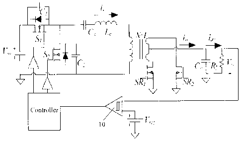
Figure 1 is a generalized schematic diagram of a series resonant converter
(SRC) with
a controller according to one embodiment;
Figure 2 is a plot of representative waveforms of an embodiment of the circuit
of
Figure 1;
Figures 3A and 3B are plots of voltage transfer characteristics for an
embodiment of
the circuit of Figure 1, for co = 1.05 and co = 1.25, respectively;
Figures 4A and 4B are plots of resonant capacitor voltage stress for an
embodiment of
the circuit of Figure 1, for co = 1.05 and o.) = 1.25, respectively;
Figures 5A and 5B are plots of resonant inductor voltage stress for an
embodiment of
the circuit of Figure 1, for co = 1.05 and co = 1.25, respectively;
Figure 6 is a plot of self resonant frequency (SRF) of a filter capacitor
cell, used to
find the required number of low-ESL capacitors for an embodiment of the
circuit of Figure 1;
Figure 7 is a plot of the number of capacitor cells as a function of filter
requirements;
Figure 8 is a plot showing waveforms during the worst-case unloading transient
for
the filter capacitor Co of an embodiment of Figure 1;
Figure 9 is a plot showing waveforms during the worst-case loading transient
for the
filter capacitor Co of an embodiment of Figure 1;
Figures 10A and 10B are plots showing impact of high threshold voltage on
filter
size: (A) for the full range of VTH; (B) for a range of VTH requiring less
than 450 uF of filter
capacitance;
Figure 11 is a plot of hysteretic window size as a function of high threshold
voltage
for a controller as described herein;
Figure 12 is a plot showing impact of clock frequency on low threshold voltage
for a
controller as described herein;
-4-
CA 02789381 2012-08-09
WO 2011/100835
PCT/CA2011/000196
Figures 13A and 13B are schematic diagrams of embodiments of a controller as
described herein;
Figure 14 shows waveforms generated from a simulation based on the controller
of
Figure 13A;
Figure 15 is a plot of current and voltage responses to a simulated transient
of an
embodiment of the circuit of Figure 1;
Figure 16 is a plot of semiconductor efficiency for a SRC with a controller
according
to an embodiment of the circuit of Figure 1;
Figure 17 is a plot of PDM duty cycle as a function of load range at 12 V
input, for a
SRC with a controller according to an embodiment of the circuit of Figure 1;
Figure 18 is a plot showing open loop results of a field programmable gate
array
(FPGA) programmed to implement an embodiment of a controller as described
herein;
Figure 19 is a plot showing output of a controller implemented with a FPGA,
with a
1.5 MHz command signal, according to one embodiment;
Figure 20 is a plot showing output of a controller implemented with a FPGA,
with a
2.5 MHz command signal; and
Figure 21 is a plot showing output of a controller implemented with a FPGA,
when
the command signal goes low in the middle of a switching cycle.
Detailed Description of Embodiments
Various techniques for controlling an SRC have been proposed. For example,
variable frequency (VF) control may be used, in which the switching frequency
of the
converter is adjusted to vary the impedance of the resonant tank, to regulate
the output
voltage. However, as the load decreases, regulation of the SRC is lost [1] and
gate loss
increases, reducing light-load efficiency.
Another control technique is constant frequency half-bridge, such as
asymmetric
pulse width modulation (APWM), where the resonant tank is fed with a unipolar
quasi-square
wave. The duty cycle of the square wave is varied to regulate the load
voltage. This
technique overcomes the regulation problem of VF control; however, it has a
limited input
-5-
CA 02789381 2012-08-09
WO 2011/100835
PCT/CA2011/000196
voltage range for which ZVS can be achieved. This technique also suffers from
problems
with gate signal generation as the duty cycle decreases from 50% [2].
Another control technique using constant frequency is secondary-side control
where
the conduction difference between the diode rectifier and the synchronous
rectifier is used to
maintain constant output voltage [4]. However, allowing diode conduction
reduces
efficiency of the converter.
A third constant frequency control technique is pulse density modulation
(PDM),
where the converter operates in bursts being fully on or fully off.
Implemented with analog
control, the PDM frequency is much greater than the switching frequency, and a
compensated
error signal is compared to a PWM waveform to determine when the converter
will be on or
off. A downfall of this method is that the output filter and control loop are
determined by the
low PDM frequency, and not the high switching frequency. Therefore, high
frequency
switching may be implemented, but without any of the associated benefits. The
most
common use of PDM is for inverters, and is implemented digitally using look up
tables [6, 8].
In such applications, output power is controlled, not voltage. By using
digital control, the
off-time is dispersed throughout the PDM cycle to minimize power fluctuations.
This
technique cannot be applied to dc/dc converters because it has similar control
delay problems
to analog implementation; and it only allows discrete power levels.
In pulse width modulation (PWM), fine output control is achieved in part by
having
fine control over the control pulse width. In conventional PDM, fine output
control is
achieved by varying the density of pulses. In one embodiment described herein,
the on time
of the converter is related to the switching frequency of the converter, such
as an integer
multiple of the switching frequency. If the switching frequency is suitably
high, a fine degree
of control is achieved. Both standard PWM and PDM control of a resonant
converter involve
operation of the converter at non-optimal conditions. However, in the
techniques described
herein, the resonant converter is operated at or close to its optimal
switching frequency.
In general, resonant converters can be classified into one of two classes
depending on
what signal transfers power. Current-type resonant converters use a sinusoidal
current; with
the most common being the series resonant converter. Voltage-type converters
transfer
power on a sinusoidal voltage; with the two most common topologies being the
parallel
resonant and series-parallel resonant converters. Application of a control
technique as
described herein is not limited to one resonant converter type or another; and
does not impede
-6-
CA 02789381 2012-08-09
WO 2011/100835
PCT/CA2011/000196
the inherent soft-switching of any resonant converter topology. In some
applications a series
resonant converter may be preferred due to its merits including: the primary-
side switches
achieve ZVS/ZCS, the rectifiers achieve ZCS, and a capacitive output filter is
used rather
than an inductive filter. Such features are topology-dependent, and
independent of the
control method used. Voltage-type converters do not have ZCS rectifiers, and
are subject to
reverse-recovery loss, which is topology-dependent.
Although embodiments are described herein mostly with respect to a half-bridge
configuration, the control method is readily extended to full-bridge circuits.
Rectifiers may
be uncontrolled (e.g., a diode) or controlled (e.g., based on a transistor,
such as a synchronous
rectifier) without impacting the fundamental behaviour of the control
technique.
The methods and circuits described herein include one or more of the following
features: regulation of the RC from no-load to full-load; response limited by
the converter
and not the control loop; inherent stability; operation in the range of tens
to hundreds of
megahertz to allow further miniaturization and integrated power architectures.
The method does not suffer from the drawbacks of prior methods, such as slow
control action or large filter requirements. The controller is implemented
digitally and may
use a clock that is a multiple of the desired switching frequency. The only
input to the
controller is the output of at least one comparator, such as a hysteretic
comparator.
According to an embodiment described herein, a SRC operated as voltage
regulator achieves
the efficiency benefits of conventional PDM control, while overcoming
drawbacks of poor
transient response and large filter size.
A generalized embodiment of a SRC with a controller as described herein is
shown in
Figure 1. In this embodiment, a hysteretic comparator 10 is used to sense the
output voltage
V, of the converter, which is compared to a reference voltage 17õ.f; and the
comparator output
is used a command signal fed to the controller. Alternatively, the output
current may be
sensed, using techniques known in the art. Current sensing may be preferred in
certain low-
current applications, such as, for example, a controller for LED lighting,
where control of the
output current is desired. Output current sensing may conveniently be
implemented in certain
converter types, such as, for example, a voltage-type converter having an
inductive output
filter, where DC resistive sensing using the resistance of the output inductor
may be used.
The controller may be implemented with one or more logic devices such as, for
example, a counter or a flip-flop. A field programmable gate array (FPGA) or a
complex
-7-
CA 02789381 2012-08-09
WO 2011/100835
PCT/CA2011/000196
programmable logic device (CPLD) may also be used. In one embodiment the
hysteretic
comparator 10 asserts a high command signal when the converter output voltage
falls below a
defined low threshold value, and sets the command signal low when the voltage
rises above a
defined high threshold value. The opposite may of course also be implemented.
The
controller produces the gating (i.e., switching) signals for the primary
switches (e.g.,
MOSFETs) at the desired switching frequency when the comparator output is
high. When
the comparator output is low, the switching cycle is ended. In one embodiment,
the
controller allows the switching cycle to complete before ending the on period.
The controller
ensures that the switching signal for each switch of the primary switch pair
(e.g., switches S1
and S2 of Figure 1) includes at least one off-on-off transition.
In another embodiment the controller produces switching signals for the
primary
switches that are one or more of edge-synchronous, opposite polarity, and 50%
duty cycle
when the command signal is high (i.e., the switching signals are symmetric).
In a further
embodiment the controller ensures proper (i.e., steady-state) RC tank behavior
if the
command signal goes low in the middle of a cycle. This is achieved by
completing the
switching cycle at the desired switching frequency. For example, the RC tank
may be driven
with an integer multiple of switching cycles, wherein pulses are not truncated
when the
controller senses the off command from the comparator (e.g., when an output
voltage of the
RC exceeds the threshold voltage). That is, the controller waits for the
switching cycle to
complete before switching off.
When transitioning the RC from off to on, the comparator output switches from
low
to high. The controller, which may include a counter, begins counting at the
next positive
clock edge. Because the clock is a multiple of the switching frequency, the
worst-case turn-
on delay is one clock cycle which is less than the switching cycle. Here,
"turn on delay"
refers to the amount of time the controller waits before enabling the RC when
an on
command is received from the hysteretic comparator. In this embodiment the
switching
frequency is related to resonant frequency, and the switching period is an
integer number of
clock periods. The PDM period is the sum of the RC on-time and off-time. When
transitioning the RC from on to off, the comparator output switches from high
to low. To
ensure a complete resonant cycle, the counter stops only if one switching
period has been
completed. Therefore, in the worst-case, the comparator output will go low
just after a cycle
has started, resulting in a one cycle delay.
-8-
CA 02789381 2012-08-09
WO 2011/100835
PCT/CA2011/000196
Representative waveforms are shown in Figure 2; where the converter is on
twice
during two different durations in the PDM period. The on intervals start and
end with zero
current transitions, while maintaining zero voltage switching in the middle.
In most prior
applications ZCS is suboptimal because it leads to frequency-dependent output
capacitance
loss. However, with the control method described herein, the frequency at
which ZCS occurs
is much lower than the switching frequency, so the loss is almost negligible.
By allowing the
converter to dictate when energy is required, reduction of the low frequency
ripple is
achieved without sacrificing response.
Control of an SRC as described herein may be analyzed by defining the output
currents according to Figure 1. The pulse density duty cycle D ppm is defined
by (1) as the
ratio of the total on time to the total on- and off-time of the SRC. This is
equal to the ratio of
load current i, to the per-cycle average of the rectified resonant tank output
current io.
I t on, k
al'
D
PDM ( 1 )
Lt
ari,k ,k
The equivalent ac resistance is a function of the pulse density duty cycle,
and defined
8/V2RL
.µac0
by (2), where 71- 2 , and N is the transformer turns ratio. The transfer
function
(0,1
Q= ______________________________________________________
is given by (3), with the variables in the equation defined as R
aco .43C. and
(4)0
03= ¨
a)r
where coo is the radian switching frequency. The definitions of the resonant
tank
parameters Q and co are identical to those used in standard converter
analyses. Thus, setting
DpDm to unity results in identical voltage transfer characteristics.
\72
=
D Prat R L
(2)
R = D R
tr ets-0
D PDM
o =
1 (3)
2N D pDm j ¨
(.0
-9-
CA 02789381 2012-08-09
WO 2011/100835
PCT/CA2011/000196
The voltage stress of the resonant components normalized to Võ, are given by
(4) and
(5). Both are inversely proportional to DpDm and are equal to the values under
traditional
control methods at unity pulse density duty cycle.
20 cs _______________________________________
I ) (4)
D faw iitker ¨ 1
V
Ls __________________________________________
V
1 (5)
_D1,01171- i+ j0 ro¨ ¨
Voltage transfer characteristics from (3) are shown in Figures 3A and 3B for
different
circuit parameters. It is shown that the gain of the circuit decreases with
increased quality
factor and relative operating frequency. It is also observed that the
influence of Q is reduced
when operating close to the resonant frequency. At unity duty cycle D pDm, the
gain is equal
to that of conventional control methods. The reduction of gain with duty cycle
illustrates the
ability to regulate the output against line and load variations through PDM
duty cycle. From
these curves, it is desirable to have a moderate value of co and a fairly high
Q to increase the
range of duty cycle required for regulation.
The limit on co is imposed by the acceptable conduction loss and required
gain. For a
given quality factor, there is a relative operating frequency that provides
the required gain
with some margin. Increasing the operating frequency beyond this requires a
lower
transformer turns ratio which increases conduction loss of the circuit.
At full load the circuit operates close to unity PDM duty cycle to keep the
conduction
loss close to that of traditional control techniques. At such operating point,
the slight increase
in conduction loss approximately cancels the slight reduction of gate loss,
which results in
efficiencies comparable to variable frequency control. However, as the load is
reduced,
frequency-dependent gate loss becomes the dominant loss component. Under light
load
conditions, the decrease in gate loss overshadows the conduction loss penalty
to make the
embodiments described herein more efficient than traditional control
techniques.
Evaluation of (4) and (5) yields component voltage stresses of the resonant
tank at
full-load, shown for G in Figures 4A and 4B, and for L, in Figures 5A and 5B,
for co = 1.05
and co = 1.25. In general, the stress increases with Q. For a given Q, the
peak stress
decreases as the operating frequency increases beyond the resonant frequency.
Therefore,
low Q and high co are desirable for minimizing component stress.
-10-
CA 02789381 2012-08-09
WO 2011/100835
PCT/CA2011/000196
From the above it will be appreciated that design of the SRC resonant tank is
a trade-
off between component stress and transfer capability. However, the voltage
stress curves are
somewhat misleading as it appears that the stress tends to infinity at low
duty cycle, which
would result in extremely oversized components. For a given set of tank
parameters, the
PDM duty cycle should be selected close to unity under the worst-case
operating conditions.
That way, the full-load stress is approximately the same as traditionally-
controlled resonant
converters, and when the duty cycle decreases with load, the peak stress
remains roughly
constant. Thus, component ratings will not increase beyond those for other
control methods.
With a control technique as described herein, there is a relationship between
hysteresis band, filter capacitor size, and clock frequency. The controller
implementation is
not limited by the clock frequency or resolution of commercially-available
programmable
logic. High clock frequency does not offer any significant improvement in
performance.
The control method and circuit described herein achieve the efficiency
benefits of
PDM without the associated high output voltage ripple, discrete output power,
or slow
response. Further, by decoupling standard control variables from the control
loop, the
method achieves practical high frequency operation, simplifies component
optimization, and
promotes miniaturization. Accordingly, the method and circuit described herein
are suitable
for applications such as central processing unit (CPU) power supplies,
particularly in
notebooks, netbooks, and other mobile devices. Implementing a series resonant
converter
that uses a control technique as described herein reduces the size and cost of
such power
supplies, as well as improves performance.
In some embodiments, when the rising edge of the comparator is used to
determine
the beginning of a switching cycle, there will be a delay in synchronizing the
switching
circuit with the system clock. The net result, limited to the first switching
cycle, is a drive-
train duty cycle greater than 50% at a slightly lower switching frequency.
Under APWM
control, drive-train duty cycle has a gain proportional to sin(nD), with the
maximum
occurring at 50% duty cycle. Operating at lower frequency increases the gain
of the tank.
The resultant gain and soft-switching capability depends on the design of the
resonant tank.
In some embodiments, if the comparator prematurely ends the switching cycle,
the net
effect will be excitation of the tank at a higher frequency, or an asymmetric
excitation of the
tank with a drive-train duty cycle less than 50%. In either case, the gain of
the resonant
network will be less than the ideal case of symmetric excitation at the
desired switching
-11-
CA 02789381 2012-08-09
WO 2011/100835
PCT/CA2011/000196
frequency. Loss of soft-switching is possible in both cases; and dependent on
resonant tank
design and the instant in the switching cycle when the turn-off signal is
applied. From the
above discussions it will be apparent that a control technique as described
herein may be
combined with one or more other techniques. For example, one such other
control method
may regulate one variable of the RC output, and a method described herein may
control a
second variable of the RC output. As an example, in half-bridge
implementations, variable
frequency, self-sustained oscillation, or asymmetric pulse width modulation
can be combined
with a method described herein. As another example, in full-bridge
implementations, phase-
shift modulation, variable frequency, self-sustained oscillation, or
asymmetric duty cycle can
be used in conjunction with a method described herein.
As another example, one such other technique can regulate against line (input
voltage)
variations, while a method as described herein may regulate against load
transients.
Therefore, instead of the converter on-time being a group of fixed-frequency,
50% duty cycle
square wave pulses, the on-time can be variable frequency symmetric pulses, or
constant
frequency asymmetric pulses; as determined by the second control loop. Further
combinations are of course possible.
The invention is further described by way of the following non-limiting
examples.
Example 1. Series Resonant Converter with Controller Implementation
This example addresses the dependency of hysteresis band, filter capacitor
size, and
clock frequency to provide rationale for the selection of each.
Analysis
Limitation of Conventional Digital Control
The limitations of digital control are a result of traditional control
techniques that rely
on fine resolution of the controller to maintain regulation. For example, (6)
and (7) are used
to calculate the required resolution and clock frequency for a buck converter.
At 500 kHz
switching frequency, a 12 V to 1 V converter with analogue to digital (ADC)
resolution of 10
-12-
CA 02789381 2012-08-09
WO 2011/100835
PCT/CA2011/000196
mV, the required resolution of the digital PWM (DPWM) is 12 bits, and the
clock frequency
is 2.05 GHz. Such requirements are impractical for low cost, low power
supplies.
1 Vin
NDpwm = 10g2(-)+ 1 = H + 1 (6)
AD AV,
fak = 2NDPwmfs (7)
However, with a control technique as described herein, the frequency variation
is due
to the number of on/off cycles, not the frequency of the driving waveform.
Further, the
hysteretic comparator acts as a single bit ADC which removes resolution and
sampling rate
requirements from the controller. This allows the control circuit to be
implemented with
extremely low clock frequencies with minimal impact on performance.
Limitations of Present-Day Capacitor Technology
The combination of high operating frequency and high current pushes the limits
of
present-day capacitor technology. As such, the effect of the equivalent series
inductance
(ESL) is more pronounced. In general, ESL is a function of the geometry of the
capacitor,
meaning larger packages will have greater ESL, as will larger capacitor values
with the same
package designation. Standard ceramic capacitors in 0805 packaging can have
ESL in the nH
range. For example, for a 22 F capacitor this translates to a self resonant
frequency (SRF)
of approximately 1 MHz. As a result, standard capacitors are ineffective above
about 500
kHz switching frequency.
To overcome the low self resonant frequency, low-ESL capacitors may be
connected
in parallel with standard capacitors to create a 'capacitor cell' with a self
resonant frequency
that is greater than the ripple frequency. A number of capacitor cells can
then be used to
form the output filter. Two options for low-ESL capacitors are reverse
geometry and multi-
terminal capacitors, with the latter offering superior reduction of ESL. The
SRF of a
capacitor cell can be calculated with (8), where capacitance and ESL are
represented by C
and l, and the subscripts std and low-ESL denote standard and low-ESL devices.
The variable
n represents the number of low-ESL capacitors used in the calculation.
_______________________________________________________ 1
SRFcell = 27T
F (Csta 4: nC/ow-ESL) (istd//
I i liow-ESL)
n
I --
(8)
-13-
CA 02789381 2012-08-09
WO 2011/100835
PCT/CA2011/000196
Evaluation of (8) produces the plot of Figure 6; where Cstd = 22 p,F, Clow-ESL
= 2.2 F, /so =
1.1 nH, and bow-ER, = 45 pH. The minimum number of low-ESL capacitors required
for a
design is determined by finding the intersection of the curve with the lowest
permissible SRF;
which is twice the switching frequency. The x-coordinate at this point or the
next highest
integer value in the event the point lies between two integers, is the minimum
number of low-
ESL capacitors required per cell. The number of cells required to at least
meet the required
filter capacitance value is found with Figure 7.
Filter Size and Hysteretic Band
The threshold voltages of the comparator, filter capacitor size, and allowable
voltage
range all impact the size and response of the converter. As with any
converter, the filter size
is limited by transient requirements. Analyses of both the loading and
unloading transients
provide a logical approach to controller implementation.
Unloading Transient Assumptions
The filter capacitor Co size is defined by (9), and determined by the
switching period
Ts., the maximum output voltage 17,,,nax, the high threshold voltage VTH, and
the capacitor
current during the maximum unloading transient (10). In (10), Aiciv,max is the
maximum load
step, and ./av is the load current. The worst case load current is the lowest
that is still
susceptible to the maximum load step. Here it is assumed that the maximum
unloading
transient only occurs at full-load. Waveforms of the worst-case unloading
transient are
shown in Figure 8 where the command signal goes low the instant after a
switching cycle has
begun. The shaded region represents the extra charge the filter capacitor has
to handle
without exceeding the maximum voltage Vo,Incoc=
Aic-0 Ts
Co =
(Vo,max VTH) (9)
DpDm
lay + lav,max (10)
.1 DpDm
The relationship between high threshold voltage and the converter
specifications and
filter size is given by (11) and was obtained by isolating VTH in (9).
-14-
CA 02789381 2012-08-09
WO 2011/100835
PCT/CA2011/000196
Aic-oTs
VTH "= Vo,max
Co (11)
Loading Transient Assumptions
The equation for the lower threshold voltage VTL is given in (12) and was
found by
assuming one clock cycle delay in synchronizing with the digital clock; as
illustrated in
Figure 9. This implementation uses a free-running clock as a means of ensuring
consistent
switching periods without issues of startup transients. However, the present
embodiment
only requires an oscillator during the on-time. From Figure 9 it can be seen
that the worst-
case loading transient occurs immediately following the start of a clock
period. In this
situation the filter capacitor must supply the charge, shown as the shaded
region, until a
switching cycle can begin the next clock cycle.
A iav,maxTclk
VTL _L Vo,min (12)
Co
Digital Clock Frequency
Unlike conventional digital controllers where high clock frequency is required
to
maintain stable operation, the present embodiment does not place strict
requirements on clock
speed. Thus the clock frequency may be relatively close to the switching
frequency. From
the above analysis, the only impact it has on transient performance is in the
case of a positive
load step. However, the filter is determined by the unloading transient, so
the impact of clock
frequency on transient response is almost negligible. It does play a role in
the size of the
hysteretic window, but only up to a certain frequency beyond which it provides
diminishing
returns.
In (13), /Ica is the ratio of a switching period 7; to a clock period Tca. The
relationship
between converter requirements and the digital clock frequency with respect to
switching
frequency is found with (13).
Ts fclk
nclk T f
= = (13)
clk o
Ai
_L av,max (v ¨ võ)
IT TL = 17o,mtn (14)
Ai- n o,max
Co clk
-15-
CA 02789381 2012-08-09
WO 2011/100835 PCT/CA2011/000196
Average Output Voltage
While the allowable operating voltage window is defined by the droop
resistance and
the rated load current, the hysteretic threshold voltages determine the
nominal output of the
converter under static load. An approximation for the nominal output voltage
is given by
(15), which is the midpoint between the threshold voltages.
,max tic ¨ 1\ DpDm
Vo,min V av
o,max ¨clk ) I av (1 ¨ D P DM rr i (15)
14),avg 2 2C0 s
Design
SRC Filter Design Based on Unloading Transient
Plots of filter capacitor size determined from (18) as a function of high
threshold
voltage are shown in Figure 10A for the full range of VTH and in Figure 10B
for a range of
VTH requiring less than 450 g of filter capacitance. The required filter size
increases
exponentially as the threshold voltage approaches the maximum output voltage.
This is
because as the allowable voltage deviation under the worst case transient is
reduced, a larger
capacitor is required to absorb the extra charge during a transient.
Clock Frequency and Filter Size
The clock frequency of the digital circuit is dependent on the loading
transient
according to (12). However, since the filter size is determined by the
unloading transient,
(14) is used to determine the allowable value of the lower threshold voltage.
Figure 11 shows
the impact of high threshold voltage on the low threshold voltage. As VTH
approaches V o,max
the low threshold voltage approaches Vo,,,,,; which is congruent with the
previous discussion
on filter size and the high threshold voltage. Referring back to Figures 10A
and 10B, a 20
mV increase in VTH from 0.96-0.98 V requires double the filter size, which
only reduces the
low threshold voltage by 3 mV for flak= 6. The low threshold voltage is
plotted against nak
in Figure 12 to justify the selection of low clock frequency. As ncik
increases, the allowable
low threshold voltage approaches the minimum output voltage. However, the
knees of the
curves occur at nak = 5, beyond which a further increase in clock frequency
loses its
effectiveness. At VTH = 0.97, increasing nem from 4 to 6 allows a 2 mV
reduction in the low
-16-
CA 02789381 2012-08-09
WO 2011/100835
PCT/CA2011/000196
threshold voltage. Such small returns may not justify arbitrary increases of
the clock
frequency. Furthermore, it shows that this implementation permits 100 MHz
switching
frequency with presently available programmable logic devices.
Converter Implementation
A series resonant converter under control as described herein, shown in Figure
1, with
the specifications given in Table I, was designed according to the above
design criteria. The
output voltage specifications were chosen to correspond to a 1 V, 40 A VR with
2 m 2 load
line. Whereas a buck converter would adapt its output voltage for a given
load, and
overshoot the upper bound during unloading transients, an SRC under this
control maintains
its output voltage within the allowable 80 mV range regardless of operating
conditions.
Table I. Series Resonant Converter Specifications
Parameter Value
Input Voltage (Vin) 12V +/-10%
Output Voltage (V0) 0.92-1.0V
Output Current (jay) 40A
Maximum Load Step 27A (40A<--->13A)
Switching Frequency (A) 5MHz
From the above design criteria, design of the resonant tank is a trade-off
between
component stress and transfer capability. Conveniently, low quality factor not
only reduces
component stress, but also improves the response of the converter.
For a given set of tank parameters, the PDM duty cycle is selected close to
unity
under the worst-case operating conditions. That way, the full-load stress is
approximately the
same as that in traditionally-controlled resonant converters, and when the
duty cycle reduces
with load, peak stress remains approximately constant. Thus, component ratings
do not
increase beyond those for other control methods.
-17-
CA 02789381 2012-08-09
WO 2011/100835
PCT/CA2011/000196
Resonant parameters of co = 1.15 and Q = 1.8 were selected for the design. At
5 MHz
switching frequency, these parameters translate to component values: Cs = 42
nF and Ls = 31
nH. For these specifications, an ideal filter capacitor requirement of 180 p,F
was calculated.
Six 22 [IF capacitors (Cs(d) in 0805 packaging with 1.1 nH ESL (istd) were
used in parallel to
form the foundation of the filter. Figure 6 was used to determine the minimum
number of
low-ESL capacitors required in each cell by finding the point on the curve
with a y-
coordinate equal to the minimum acceptable SRF value. The x-coordinate of this
point or the
next highest integer value in the event the point lies between two integers,
is the minimum
number of low-ESL capacitors required per cell. The number of cells required
to at least
meet the required filter capacitance value was found with Figure 7 simply by
using the result
from Figure 6 along the x-axis and reading the corresponding y-value. Thus, in
this design
six low-ESL capacitors were required per capacitor cell, and six cells were
required for the
filter to obtain a self resonant frequency of the filter above 10 MHz.
Controller Simulation
A controller based on the above design criteria was implemented in Altera
Quartus II software (Altera Corporation, San Jose, California). The schematic
is shown in
Figure 13B. Results of the simulation are shown in Figure 14. The key
waveforms are the
100 MHz system clock, clk 1 (line 0); the controller clock, PLL clk (line 2);
the command
signal, cmd (line 3); and controller output, PWM (line 9). Time instants ti
and t2 are
indicated to show that the output behaves as expected. At ti the command
signal goes high in
the middle of a clock cycle, but the PWM output does start until the next
rising edge of the
PLL_clk. At t2 the command signal falls shortly after a PWM cycle begins;
however, the
cycle continues to maintain constant switching frequency.
Converter Simulation
Simulation results are shown in Figure 15. A total of 211.2 p.F of filter
capacitance
was used to achieve these results, which is only that high due to limitations
of current
capacitor technology. Improvements in capacitor technology will enable further
miniaturization through filter size reduction with this control technique. In
comparison, a
two-phase buck converter (L = 300 nH) would require 700 pf of capacitance to
obtain the
same results; i.e., 3.3 times more capacitance than a practical SRC. In Figure
16, the
-18-
CA 02789381 2012-08-09
WO 2011/100835
PCT/CA2011/000196
semiconductor efficiency results are shown for the simulated converter across
the load range;
assuming full recovery of the gate energy of the synchronous rectifiers. Soft-
switching and
pulsed operation maintains efficiency greater than 91% across the load range.
Further, the
efficiency increases with load reduction, which is the contrary to typical
converter behaviour.
This can be explained by Figure 17 where the duty cycle is shown across the
operating range
of the converter. At light load, the conduction loss is reduced through
natural current
reduction and increased off-time of the converter; as well as through the
maintenance of soft-
switching. While transformer losses and conduction loss of the traces and
resonant and filter
capacitors are not accounted for, symmetrical constant frequency operation of
the converter
minimizes these as well.
Experimental Results
An Altera UP3 Education Board with EP1C6Q240C8 CycloneTM field
programmable gate array (FPGA) (Altera Corporation, San Jose, California) was
programmed to implement a controller based on the above design criteria. The
schematic is
shown in Figure 13A, and includes a phase locked loop (PLL). The PLL was
available on the
FPGA and was conveniently used as a clock divider, which was needed because of
the high
frequency clock (100 MHz) provided on the FPGA. Those skilled in the art will
know of
other ways to make a lower frequency clock from a high frequency clock. The
PLL or other
clock divider may be eliminated where a lower frequency clock (e.g., 4X the
switching
frequency) is available (see Figure 13B).
To verify correct operation of the controller, command signals of varying
frequencies
were fed into the FPGA, and the resulting PWM signal was measured. The top
trace in
Figures 18 to 21 is the 100 MHz clock generated by an on-board oscillator. The
second trace
is the phase-locked loop (PLL) output, which acts as the clock for the
designed logic. A
clock frequency of 20 MHz (nak = 4) was chosen based on the results of the
analysis
presented above. As shown in Figure 18, the PWM signal (third trace) is active
when the
command signal (bottom trace) is high; and inactive otherwise. To highlight
the speed of the
controller, the results for 1.5 MHz and 2.5 MHz command signals are shown in
Figures 19
and 20, respectively. In Figure 21 it can be seen that the controller output
maintains a
constant switching frequency despite the command signal falling shortly after
the switching
cycle begins.
-19-
CA 02789381 2015-05-04
Equivalents
While the invention has been described with respect to illustrative
embodiments
thereof, it will be understood that various changes may be made to the
embodiments without
departing from the scope of the invention. Accordingly, the described
embodiments are to be
considered merely exemplary and the invention is not to be limited thereby.
-20-
CA 02789381 2012-08-09
WO 2011/100835
PCT/CA2011/000196
References
[1] R.L. Steigerwald, A Comparison of Half-Bridge Resonant Converter
Topologies, IEEE
Trans. Power Elec., vol. 3, pp. 174-182, April 1988.
[2] P.K. Jain, A. St-Martin, and G. Edwards, Asymmetrical pulse-width-
modulated resonant
DC/DC converter topologies, IEEE Trans. Power Elec., vol. 11, pp. 413-422, May
1996.
[3] P. Jain, Asymmetrical PWM Resonant DC/DC Converter, Canadian Patent No.
2,080,027, November 1997.
[4] S. Pan, and P.K. Jain, Secondary-side adaptive digital controlled series
resonant dc-dc
converters for low voltage high current applications, in Proc. Power Elec.
Specialists
Conf, pp. 711-717, 2008.
[5] S. Dalapati, S. Ray, S. Chaudhuri, and C. Chakraborty, Control of a series
resonant
converter by pulse density modulation, in Proc. IEEE India Annual Conf
(INDICON), pp. 601-604, 2004.
[6] H. Fujita, H. Akagi, K. Sano, K. Mita, and R.H. Leonard, Pulse density
modulation based
power control of a 4 kW 400 KHz voltage-source invertor for induction heating
applications, in Proc. Power Conversion Conf, pp. 111-116, 1993.
[7] H. Koizumi, K. Kurokawa, and S. Mori, Analysis of class d inverter with
irregular driving
patterns, IEEE Trans. Circuits and Sys., vol. 53, pp. 677-687, March 2006.
[8] Y.-H. Liu, S.-C. Wang, Y.-F. Luo, Digital dimming control of CCFL drive
system using
pulse density modulation technique, in Proc. IEEE Region 10 Conf, pp. 1-4,
2007.
[9] D.D-C Lu, J.C.P. Liu, F.N.K. Poon, and B.M.H. Pong, A Single phase voltage
regulator
module (VRM) with stepping inductance for fast transient response, IEEE Trans.
Power Elec., vol. 22, pp. 417-424, March 2007.
[10] X. Wang, I. Batarseh, S.A. Chickamennahalli, and E. Standford, VR
transient
improvement at high slew rate load-active voltage transient voltage
compensator,
IEEE Trans. Power Elec., vol. 22, pp. 1472-1479, July 2007.
[11] D.J. Tschirhart, and P.K. Jain, A CLL resonant asymmetrical pulse width-
modulated
converter with improved efficiency, IEEE Trans. Industrial Elec., vol. 55, pp.
114-
122, January 2008.
-21-