Note: Descriptions are shown in the official language in which they were submitted.
CA 02789514 2012-08-10
STEP SWITCH
The invention relates to a tap changer with semiconductor
switching elements for uninterrupted switching over between winding
taps of a tapped transformer.
s A tap changer with semiconductor switching elements,
which is constructed as a hybrid switch, is known from WO 01/22447.
This known tap changer has, as hybrid switch, a mechanical part and
an electrical part. The mechanical part, which is the actual
subject of WO 01/22447, has mechanical switching contacts; the
central part is a movable slide contact that is moved along a
contact guide rail, which is connected with the star point, by
means of a motor drive and in that case connects stationary contact
elements. The actual load changeover itself is carried out by two
IGBTs each with four diodes in a Graetz circuit. This known
concept of a hybrid switch is subject to high mechanical loading in
order to ensure the necessary load changeover precisely at the zero
transition of the load current.
A further IGBT switching device is known from WO
97/05536, in which the taps of the regulating winding of a power
transformer are connectable with a load shunt by way of a series
circuit of two IGBTs. However, in this arrangement it is necessary
to undertake a special adaptation of the tap changer to the
respective tapped transformer that is to be connected.
The object of the invention is to indicate a tap changer
of the kind stated in the introduction that is of simple
construction and has a high level of functional reliability.
Moreover, it is an object of the invention to indicate such a tap
changer that is usable as standard apparatus for the most diverse
tapped transformers without transformer-specific adaptation being
needed.
- 1 -
CA 02789514 2012-08-10
These objects are fulfilled by a tap changer with the
features of the first patent claim. The subclaims relate to
particularly advantageous developments of the invention.
The invention starts from two semiconductor switching
units, wherein each switching unit has two IGBTs in anti-parallel
connection. Associated with each individual IGBT is a varistor
connected in parallel therewith. In that case, the varistor is so
dimensioned that the varistor voltage is smaller than the maximum
blocking voltage of the respective parallel IGBTs, but greater than
the maximum instantaneous value of the tap voltage.
As is usual in the case of tap changers of the hybrid
type, the semiconductor switching units are switchable on and off
by mechanical contacts and are connectable with the load shunt.
The invention shall be explained in more detail in the
following by way of drawings, in which:
Figure 1 shows a tap changer according to the invention
in schematic illustration,
Figure la shows an enlarged detail illustration of the
semiconductor switching units shown in Figure 1,
Figure 2 shows a tap changer according to the invention
in schematic illustration with an alternative contact construction,
Figure 3 shows a switching sequence in the case of
switching over from one winding tap n to an adjacent winding tap
n+l,
Figure 4 shows a realization, in terms of apparatus, of a
tap changer according to the invention in schematic illustration,
Figure 5 shows the constructional form of such a tap
changer according to the invention in perspective illustration,
Figure 6 shows a lateral sectional illustration thereof
and
- 2 -
CA 02789514 2012-08-10
Figure 7 shows a movable contact carrier of such a tap
changer by itself in perspective illustration.
Figure 1 shows a tap changer according to the invention.
Illustrated here are two load branches A and B that are connectable
s with two winding taps with tapped transformer by a respective
mechanical contact. Each of the two load branches A and B has a
mechanical main contact MCa or MCb, which in stationary operation
conducts the current of the respectively connected load branch and
produces a direct connection with a load shunt LA. Each load
branch A and B has in parallel with the respective main contact MCa
or MCb a series circuit consisting of a further mechanical contact
TCa or TCb as well as a respective semiconductor switching unit
SCSa, SCSb. The semiconductor switch units SCSa, SCSb are
electrically connected together at the side remote from the
respective switch contacts TCa, TCb and lead to a mechanical
transfer contact TC, the other side of which is connected with the
load shunt LA. Thus, during the switching over, which will be
explained in more detail further below, it is possible by
appropriate actuation of the mechanical contact TCa or TCb as well
as of the transfer contact TC to produce an electrical connection
of each of the two load branches A and B by way of the respective
semiconductor switching unit SCSa or SCSb with the load shunt LA.
Figure la additionally shows the electronic subassemblies
respectively shown on the right in Figure 1 and later also in the
following Figure 2, i.e. semiconductor switching units SCSa, SCSb,
in enlarged illustration. In that case, four IGBTs Ti ... T4 are
shown, of which two are connected in series relative to one another
in each branch. In addition, a diode D1 ... D4 is provided in
parallel with each IGBT Ti ... T4, wherein the diodes (D1, D2; D3,
D4) in each branch are connected relative to one another.
- 3 -
CA 02789514 2012-08-10
Moreover, a respective varistor Varl ... Var4 is in addition
connected in parallel therewith.
The two semiconductor switching units SCSa, SCSb
represent the actual semiconductor switch SCS. It consists, as
already explained, of the following components: in total four IGBTs
Ti ... T4 are provided, of which two are in each path. The IGBTS
are activated in pairs. If the load branch or path A is the side
switching off, initially the IGBTS Ti and T2 are switched on.
Since the current direction at the switch-over instant is random,
the IGBTS are connected in series relative to one another. During
the switching over to the other load branch or path B, the IGBTS 1
and 2 are switched off and the IGBTS of the other side are switched
on almost simultaneously. Diodes D1 ... D4 are provided in
parallel with each IGBT Ti ... T4. In addition, a respective
varistor Varl ... Var4 is also connected in parallel therewith.
These varistors serve for discharging or charging the stray
impedances (stray inductances) of the transformer stage. It can be
seen that the electrical circuit of the semiconductor switch SCS in
each branch A or B is of identical construction and contains the
described semiconductor switching units SCSa and SCSb. The
electrical combination can be seen in the lower part of Figure 1a,
which leads to the transfer contact TC explained further above and
not illustrated here.
Figure 2 shows a tap changer according to the invention
with, again, two load branches A and B. The already explained
mechanical contacts TCa, TCb and TC are here constructed as doubled
interrupting contacts.
Figure 3 shows a switching sequence in the case of
switching over of the tap changer from n to n+1. In that case, the
following steps are executed:
- 4 -
CA 02789514 2012-08-10
Phase 1: Stationary operation at tap A. The current
flows via the closed contact MCa to the load shunt
LA. The semiconductor switching units SCSa, SCSb
remain switched off, since all other mechanical
switches are open.
Phase 2: Switching-on of the electronic system. The
mechanical contacts TCa, TCb and TC are switched on
almost simultaneously. The semiconductor switch SCS
is thus supplied with electrical energy by way of
the tap voltage.
Phase 3: Switching-on of the semiconductor switching
subassembly SCSa. Since the electrical resistance
of the mechanical contact group is low by comparison
with that of the semiconductor components and of the
remaining electronic components the current is
initially still conducted by way of the mechanical
contact Mca.
Phase 4: Opening of the main contact MCa. The current is
thereby conducted by way of the semiconductor
switching unit SCSa.
Phase 5: The electronic system switches over. The
semiconductor switching unit SCSa is switched off;
the semiconductor switching unit SCSb is switched on
and takes over conducting of current.
Phase 6: The mechanical contact MCb of the other side B
is switched on and now takes over conducting the
current.
Phase 7: Switching-off of the semiconductor switching
unit SCSb. As soon as the mechanical contact MCb is
closed, the electronic system switches off the
semiconductor switching unit SCSb of this branch.
- 5 -
CA 02789514 2012-08-10
Phase 8: Switching-off of the entire electronic system.
The mechanical contacts TCa, TCb and TC are for that
purpose switched off almost simultaneously. All
electronic components are isolated from the voltage
supply, i.e. the tap voltage. The load current is
conducted from the side B via the closed mechanical
main contact MCb directly to the load shunt LA. The
switching over is concluded; the new static state is
reached.
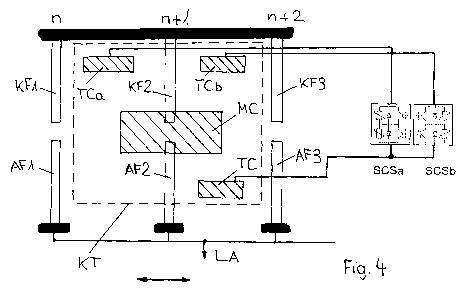
Figure 4 shows a form of realization of the tap changer
according to the invention, which is schematically illustrated in
Figures 1 and 2 and that executes the switching sequence, which is
illustrated in Figure 3, at the time of switching over.
In that regard, winding taps, here n, n+1, n+2., are
again shown, which are electrically connected with elongate, thin
pencil-like fixed contact fingers KF1 ... KF3. These contact
fingers KF1 ... KF3 are provided opposite respective further,
similarly constructed elongate contact fingers AF1 ... AF3 as shunt
fingers, which are conductively connected together and form the
load shunt LA. Provided above the contact fingers KF1 ... KF3 and
AF1 ... AF3, which lie horizontally in a plane, on both sides is a
contact carrier KT that is here indicated by dashed lines and that
is movable perpendicularly to the length direction of the contact
fingers. The movement direction is again symbolized by an arrow.
Arranged on the contact carrier KT on the side facing the
contact fingers KF1 ... KF3; AF1 ... AF3 are contact members that
are fixed on the contact carrier KT and are moved therewith in
invariable geometric arrangement relative thereto. In that case,
on the one hand this is the contact member MC that connects the
respective winding tap directly in stationary operation - which is
shown in Figure 4 - with the opposite contact finger of the load
- 6 -
CA 02789514 2012-08-10
shunt LA. On the other hand, two separate further contact members
TCa and TCb arranged laterally and symmetrically with respect
thereto are provided. The contact member TCa is electrically
connected with the input of the first semiconductor switching unit
SCSa. The second contact member TCb is electrically connected with
the input of the second semiconductor switching unit SCSb.
Finally, a further contact member TC that is electrically connected
with the output of the two semiconductor units SCSa, SCSb is
additionally provided on the other side on the contact carrier KT.
The explained further contact members - apart from the contact
member MC - are geometrically so arranged that depending on the
respective switching direction, the contact member TCa or TCb
temporarily contacts one of the contact fingers KF1 ... KF3 when
the contact carrier KT moves. The contact member TC on the other
side is geometrically arranged in such a manner that it produces
temporary contact with one of the contact fingers AF1 ... AF3 of
the load shunt LA during a switching-over process, i.e. actuation
of the contact carrier KT. In stationary operation, all these
contact members TCa, TCb, TC are not connected; the electrical
connection directly from the respectively connected winding tap,
here n+l, to the load shunt LA takes place exclusively by the
contact member MC, whilst the entire electronic system is cleared.
The construction, which is shown in this embodiment, of the
contacts - which are narrow in movement direction - as contact
fingers in conjunction with the movable contacts - which are wide
in movement direction - respectively constructed as a contact
member makes possible overall a particularly advantageous,
voltage-resistant form of the tap changer according to the
invention.
- 7 -
CA 02789514 2012-08-10
The designation of the explained contact members in this
figure corresponds with the designation of the mechanical switches
in Figures 1 and 2, which they represent.
It is to be noted that regardless of the constructional
form the circuit according to Figure 1 or 2 and also the switching
sequence according to Figure 3 remain unchanged.
Figure 5 shows, in schematic perspective illustration,
the constructional form. A housing 1 with an upper housing support
2 is shown. A contact carrier 3, which is linearly displaceable in
longitudinal direction of the housing 1 and that was designated in
Figure 4 as KT, is illustrated. The contact carrier 3 will be
discussed in more detail later. Contact fingers 4 are provided in
a first horizontal plane el, which is indicated by a dot-dashed
line and that are designated KF in Figure 4. Further contact
fingers 5 are arranged respectively opposite as shunt fingers and
are denoted AF in Figure 4. All shunt fingers 5 are electrically
connected together by means of a connecting plate 6 and led to the
load shunt. Contact fingers 7 are arranged in a second horizontal
plane e2, which is arranged parallel thereto, and on a side of the
housing 1, further contact fingers 8 are arranged in the center on
a separate carrier and further contact fingers 9 are arranged on
the other side again in the second horizontal plane e2.
It is to be noted that all contact fingers 4, 5; 7, 8, 9
are arranged at the same grid spacing; in each instance, for
reasons of clarity only one of each kind of the contact fingers is
provided with reference numerals. The contact carrier 3 has at its
lower region a two-part main contact 10 as contact member MC, which
at the respectively opposite, corresponding contact finger 4 is
electrically connected with the respective shunt finger 5 and thus
produces in stationary operation a direct connection with the load
shunt, as is shown in Figures 1 and 2.
- 8 -
CA 02789514 2012-08-10
The contact fingers 7 are respectively electrically
connected with the input of the first semiconductor switching unit
SCSa. The contact fingers 8 are respectively connected with the
input of the second semiconductor switching unit SCSb. Finally,
the contact fingers 9 are electrically connected with the common
output of the two semiconductor switching units SCSa, SCSb.
These electrical connections are, in fact, shown in
Figure 4, but here for reasons of clarity not illustrated in Figure
5, any more than the drive of the contact carrier 3.
Figure 6 shows this arrangement in lateral sectional
illustration. It can be clearly seen here that the contact fingers
4 and 5 are arranged in a first horizontal plane el and the contact
fingers 7, 8, 9 in a second horizontal plane e2. It can also be
seen that the contact carrier 3 has, apart from the described main
is contact 10, contact members 11, 12 and 13, which respectively
co-operate, i.e. can be connected, with the contact fingers 7 or 8
or 9, in the upper region.
The contact carrier 3 has at its lower part further
contact members 14, 15. Contact member 14 can connect the
respective contact finger 4; contact member 15 can connect the
respective contact finger 5. It is important for the function that
the contact members 11 and 12 are electrically connected with the
contact member 14, whereagainst the contact member 13 is
electrically connected with the contact member 15. The contact
carrier 3 thus connects electrical contact members 11, 12, 13 of
the upper plane e2 with contact members 14, 15 of the lower plane
el in an entirely specific manner. In this form of embodiment of
the invention as well, the contact fingers 4, 5; 7, 8, 9 are
constructed as pencil-like contact fingers that are narrow as seen
in movement direction of the contact carrier and that are fastened
only at one end, whereas the contact members 11, 12, 13; 14, 15 as
- 9 -
CA 02789514 2012-08-10
well as the main contact 10 have a substantially larger length,
preferably at least three times, in movement direction of the
contact carrier 3.
Figure 7 shows a contact carrier 3 by itself in
perspective illustration. Here at the outset the lateral contact
members 14, 15 arranged in the lower horizontal plane as well as
the main contact 10 can be seen. The contact members 11, 12 and
13, which are laterally offset in movement direction (indicated by
an arrow), are shown in the upper horizontal plane. The contact
member 11 corresponds in its function with the contact TCa: it
produces the connection with the input of the first semiconductor
switching unit SCSa. The contact member 12 corresponds with a
contact TCb: it produces the connection with the input of the
second semiconductor switching unit SCSb. The contact member 13
corresponds with the contact TC: it produces the connection with
the common output of the two semiconductor switching units SCSa,
SCSb. Precisely the electrical and mechanical construction
schematically illustrated in Figure 4 is thus realized.
On movement of the contact carrier 3 the first or second
semiconductor switching unit SCSa or SCSb, depending on the
respective switching direction, is supplied with electrical energy
by way of the respective contact member 11, corresponding with TCa,
or 12, corresponding with TCb, which is respectively temporarily
electrically connected with a fixed tap contact. The common output
of the semiconductor switching units SCSa and SCSb is then led by
way of the contact member 13, corresponding with TC, back again to
the load shunt.
In the embodiment, two horizontal planes were described;
it is equally also possible within the scope of the invention to
vertically arrange the two planes, which run in parallel.
- 10 -
CA 02789514 2012-08-10
In summary, the function of the contact carrier 3 can be
described in the following terms: In stationary operation it
produces a direct connection of a winding tap with the load shunt
in that a corresponding contact finger 4 is electrically connected
with the corresponding contact finger 5 of the load shunt by the
main contact 10. During the switching over, thereagainst, this
direct contacting is interrupted and the respective semiconductor
switching unit SCSI or SCS2 is temporarily switched on by contact
member 11 or 12 in another horizontal plane and the (common) output
of that switching unit is led by the further contact member 13 back
again in the first horizontal plane to the contact member 15 and on
to the contact finger 5 of the load shunt 6. The actual switching
planes, i.e. the horizontal planes el, are characteristic, as is
the auxiliary switching plane, i.e. the plane e2, for temporary
switching-on of the semiconductor switching units during a
switching-over process.
- 11 -