Note: Descriptions are shown in the official language in which they were submitted.
CA 02789658 2012-08-13
WO 2010/114736
PCT/US2010/028255
OPTICAL SPECTROSCOPY DEVICE FOR NON-INVASIVE BLOOD
GLUCOSE DETECTION AND ASSOCIATED METHOD OF USE
BACKGROUND OF THE INVENTION
[0001] Diabetes is a chronic disease that, when not controlled, over
time leads to
serious damage to many of the body's systems, including the nerves, blood
vessels,
eyes, kidneys and heart. The National Institute of Diabetes and Digestive and
Kidney
Diseases (NIDDK) estimates that 23.6 million people or 7.8 percent of the
population
in the United States had diabetes in 2007. Globally, the World Health
Organization
(WHO) estimates that more than 180 million people have diabetes, a number they
expect to increase to 366 million by 2030, with 30.3 million in the United
States.
According to the WHO, an estimated 1.1 million people died from diabetes in
2005.
They project that diabetes deaths will increase by more than 50% between 2006
and
2015 overall and by more than 80% in upper-middle income countries.
[0002] The economic burden from diabetes for individuals and society as
a whole is
substantial. According to the American Diabetes Association, the total annual
economic cost of diabetes was estimated to be $174 billion in the United
States in
2007. This is an increase of $42 billion since 2002. This 32% increase means
the
dollar amount has risen over $8 billion more each year.
[0003] A vital element of diabetes management is the self-monitoring of
blood
glucose (SMBG) concentration by diabetics in the home environment. By testing
blood glucose levels often, diabetics can better manage medication, diet, and
exercise
to maintain control and prevent the long-term negative health outcomes. In
fact, the
Diabetes Control and Complications Trial (DCCT), which followed 1,441
diabetics
for several years, showed that those following an intensive-control program
with
multiple blood sugar tests each day as compared with the standard-treatment
group
had only one-fourth as many people develop diabetic eye disease, half as many
develop kidney disease, one-third many develop nerve disease, and far fewer
people
who already had early forms of these three complications got worse.
[0004] However, current monitoring techniques discourage regular use
due to the
inconvenient and painful nature of drawing blood through the skin prior to
analysis,
which causes many diabetics to not be as diligent as they should be for good
blood
1
CA 02789658 2016-09-28
glucose control. As a result, non-invasive measurement of glucose
concentration is a desirable and beneficial development for the management
of diabetes. A non-invasive monitor will make testing multiple times each
day pain-free and more palatable for children with diabetes. According to a
study published in 2005 (J, Wagner, C. Malchoff, and G. Abbott, Diabetes
Technology & Therapeutics, 7(4) 2005, 612 ¨ 619), people with diabetes
would perform SMBG more frequently and have improved quality of life
with a non-invasive blood glucose monitoring device.
[0005] There exist a number of non-invasive approaches for blood glucose
determination. One technique of non-invasive blood chemicals detection
involves collecting and analyzing light spectra data.
[0006] Extracting information about blood characteristics such as glucose
concentration from spectral or other data obtained from spectroscopy is a
complex problem due to the presence of components (e.g., skin, fat, muscle,
bone, interstitial fluid) other than blood in the area that is being sensed.
Such
other components can influence these signals in such a way as to alter the
reading. In particular, the resulting signal may be much larger in magnitude
than the portion of the signal that corresponds to blood, and therefore limits
the ability to accurately extract blood characteristics information.
SUMMARY OF THE INVENTION
[0006a] In accordance with an embodiment of the present invention, there is
provided an optical spectroscopy apparatus, the apparatus comprising: a light
concentrating portion having: a) a first outer wall having an anterior end, a
posterior end, an inner surface and an outer surface, the inner surface
defining an interior portion, the interior portion having an anterior end and
a
posterior end; and b) a light source disposed within the interior portion. The
first outer wall has an opening in the posterior end, the opening having an
opening diameter. The interior portion has a substantially frusto-conical
shape; wherein the interior portion has a cross-sectional diameter at the
opening equal to the opening diameter and a second cross-
2
CA 02789658 2016-09-28
sectional diameter near the anterior end that is less than the opening
diameter. The inner surface is photo-reflective, wherein the interior portion
is structured to concentrate light before the light is received by a condenser
lens.
[0006b] Another embodiment of the present invention provides a method for
concentrating light in an optical spectroscopy apparatus, the method
comprising: utilizing a light source located with an interior portion of a
first
outer wall, wherein the first outer wall includes an anterior end, a posterior
end, a photo-reflective inner surface and an outer surface, the inner surface
defining an interior portion, the interior portion having an anterior end and
a
posterior end is substantially frusto-conical shape and the first outer wall
has
an opening in the posterior end, the opening having an opening diameter and
the interior portion has a cross-sectional diameter at the opening equal to
the
opening diameter and a second cross-sectional diameter near the anterior end
that is less than the opening diameter; and enhancing light power of light
before the light is received at a condenser lens by concentrating the light
using the structure of the interior portion.
BRIEF DESCRIPTION OF THE DRAWINGS
[0007] In the drawings, which are not necessarily drawn to scale, like
numerals
describe substantially similar components throughout the several views.
Like numerals having different letter suffixes represent different instances
of
substantially similar components. The drawings illustrate generally, by way
of example, but not by way of limitation, various embodiments discussed in
the present document.
FIG. 1 illustrates a plot of a pulse wave corresponding to light absorption
of arterial blood, according to some embodiments;
FIG. 2 is a simplified block diagram that illustrates the components of an
optical measurement system according to the present invention;
FIG. 3 illustrates an existing optical configuration for performing optical
measurements of a biological sample, according to soine embodiments;
2a
CA 02789658 2016-09-28
[0011] FIG. 4A illustrates a first alternative embodiment for performing
optical
measurements of a biological sample;
[0012] FIG. 4B illustrates a preferred embodiment for performing optical
measurements of a biological sample;
[0013] FIG. 4C illustrates a second alternative embodiment for performing
optical
measurements of a biological sample;
[0014] FIG. 5 is a cross-sectional view of an exemplary light funnel and
half angle
(a); and
[0015] FIG. 6 is a cross-sectional view of an exemplary light funnel and
light source.
DETAILED DESCRIPTION OF THE INVENTION
[0016] The following detailed description includes references to the
accompanying
drawings, which form a part of the detailed description. The drawings show, by
way
of illustration, specific embodiments in which the invention may be practiced.
These
embodiments, which are also referred to herein as "examples," are described in
enough detail to enable those skilled in the art to practice the invention.
The
embodiments may be combined, other embodiments may be utilized, or structural,
and logical changes may be made without departing from the scope of the
present
invention. The following detailed description is, therefore, not to be taken
in a
limiting sense, and the scope of the present invention is defined by the
appended
claims and their equivalents.
[0017] In this document, the terms "a" or "an" are used to include one or
more than
one and the term "or" is used to refer to a nonexclusive "or" unless otherwise
indicated. In addition, it is to be understood that the phraseology or
terminology
employed herein, and not otherwise defined, is for the purpose of description
only and
not of limitation. In the event of inconsistent usages between this document
and the
prior art documents referred to herein, the usage in the prior art references
should be
considered supplementary to that of this document; for irreconcilable
inconsistencies,
the usage in this document controls.
3
CA 02789658 2012-08-13
WO 2010/114736
PCT/US2010/028255
[0018] Embodiments of the present invention relate to optical
components, such as
light funnels for illumination and measurement of optical properties of a
sample.
Although spectroscopic sampling of human or animal body regions are
exemplified,
the embodiments relate to all types of optical instrumentation, including
optical
detectors, microscopes, spectrometers, etc.
[0019] Optical spectroscopy can be used to determine the amount of
light absorbed by
a biological sample such as human finger. By measuring the amount of light
absorbed by the finger, it is possible to determine glucose, cholesterol, and
hemoglobin levels of a person non-invasively. Fingertip measurements are
usually
preferred because of the large concentration of capillaries in the fingertip
and because
of the conversion of arterial blood into venous blood that occurs in the
fingertip.
However, the techniques of the present invention are not limited to use with a
human
finger. For example, the use of other samples, such as a human earlobe, may be
desirable.
[0020] When light is transmitted through a biological sample, such as a
human finger,
the light is absorbed and scattered by various components of the finger
including skin,
muscle, bone, fat, interstitial fluid and blood. It has been observed,
however, that
light absorption by a human finger exhibits a small cyclic pattern that
corresponds to a
heartbeat. FIG. 1 depicts a plot 102 of a cyclic detector photocurrent, D (t)
, that
corresponds to the light absorption of arterial blood in the capillary due to
the
heartbeat of the user. Although the magnitude of the cyclic pattern is small
in
comparison to the total photocurrent generated by the detector, considerable
information can be extracted from the cyclic pattern of the plot 102. For
example,
assuming that the person's heart rate is sixty beats per minute, the time
between the
start of any pulse beat and the end of that pulse beat is one-second. During
this one-
second period, the photocurrent will have a maximum or peak 104 reading and
minimum or valley 106 reading. The peak 104 reading of the plot corresponds to
when there is a minimum amount of blood in the capillaries, and the valley 106
reading corresponds to when there is a maximum amount of blood in the
capillaries.
By using information provided by the peak and valley of the cyclic plot, the
optical
absorption and scattering by major finger constituents that are not in the
capillaries
such as skin, fat, bones, muscle, and interstitial fluids are excluded. These
major
4
CA 02789658 2012-08-13
WO 2010/114736
PCT/US2010/028255
constituents that are not in the capillaries are excluded because they are not
likely to
change during the time interval of one heartbeat. In other words, the light
that is
absorbed by the blood can be detected based on the peaks and valleys of the
plot 102.
[0021] Assuming that the peak of the cyclic photocurrent generated by
the light-
sensing device is 4, the adjacent valley of the cyclic photocurrent is Iv, and
the
photocurrent generated by the light-sensing device without a sample is /0, the
transmittances corresponding to the peak and valley photocurrents can be
defined as:
[0022] T¨ (1);
v
[0023] and
[0024] T =¨ (2);
P
[0025] The corresponding peak and valley absorbance are:
[0026] Av = ¨log(Tv) (3);
[0027] and
[0028] Ap =¨log(T) (4);
[0029] The difference between AN and Ap reflects the light absorption
and scattering
by only the blood in the finger:
r /
[0030] EA=Av ¨ Ap= log ¨P (5);
/v
[0031] The algorithm shown in equation (5) only requires monitoring
the
photocurrent corresponding to light power transmitted through the finger. As a
result,
there is no need to determine photocurrent generated by the light-sensing
device
without a human finger.
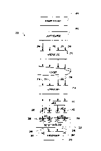
[0032] FIG. 2 is a simplified block diagram that illustrates components
of a current
optical measurement system, which is generally indicated by numeral 200, which
uses
the "pulsatile" concept for determining an amount of light absorbed and
scattered
solely by the blood in a sample (e.g. human finger). A power source 201, such
as a
battery, provides power to a light source 202 that generates a plurality of
light beams
204, 206, 208, 210 that are directed toward the top of the finger of a user.
According
to one aspect of the optical measurement system 200, each of the light beams
204,
CA 02789658 2012-08-13
WO 2010/114736
PCT/US2010/028255
206, 208, 210 have the same wavelength range, typically from about 700 nm to
about
1600 nm. Although the optical measurement system 200 is described herein as
generating four (4) light beams, it is contemplated that the light source 202
can be
altered to generate fewer light beams or additional light beams in other
embodiments.
[0033] A first aperture 212 ensures that the light beams 204, 206,
208, 210 strike a
target area of the sample (e.g. human finger). A second aperture 214 ensures
that the
portion of the light beams that are transmitted through the sample strike a
lens 216.
Light beams 204, 206, 208, 210 are attenuated by the sample and components of
the
optical measurement system 200, and, thus, attenuated light beams 218, 220,
222, 224
are emitted from the sample. The attenuated light beams 218, 220, 222, 224
strike the
lens 216, and the lens 216 collects the attenuated light beams 218, 220, 222,
224 so
that they impinge more efficiently on a detector block 226.
[0034] The detector block 226 is positioned directly under the lens
216 and comprises
a plurality of light-sensing devices (LSD) 228, 230, 232, 234 such as an array
of
photodiodes. According to one aspect of the optical measurement system 200,
each
of the light-sensing devices 228, 230, 232, 234 is tuned to detect a specific
spectrum
(or spectrums) of light. For example, each light-sensing device may be
associated
with a corresponding interference filter (IF), such as filters 236, 238, 240,
242. An
interference filter transmits one or more spectral bands or lines of light,
and
substantially blocks others.
[0035] Each of the light-sensing devices 228, 230, 232, 234 generates
a
corresponding photocurrent signal 244, 246, 248, 250 that is proportional to
the power
of the light received by the particular light sensing device. The photocurrent
signal
generated by the photodiode can be converted to another form of signal, such
as an
analog voltage signal or a digital signal.
[0036] Processor 243 is coupled to the detector block 226 and is
configured to
calculate the change of photocurrent signals 244, 246, 248, 250. In an
exemplary
embodiment, processor 243 executes an algorithm such as shown in the Equation
indicated by numeral (5) above, to calculate the change in the light
absorption (AA)
solely caused by the blood in the finger. Thereafter, this quantitative
calculation of
light absorption of the blood can be used to determine a characteristic of the
blood.
For example, by comparing the calculated light absorption value to
predetermined
6
CA 02789658 2012-08-13
WO 2010/114736
PCT/US2010/028255
values corresponding to different glucose levels stored in a memory (not
shown), a
glucose level of the user can be determined.
[0037] A difficulty associated with the finger based pulsatile
detection methodology
is low signal-to-noise ("S/N") ratio, because the amplitude of cyclic pattern
(i.e., the
difference between peak and valley) is typically 1%-2% of the total photocun-
ent
generated by the light power transmitted through the sample (e.g. a person's
finger).
To obtain a S/N ratio of 100:1 in the determination of AA, the baseline noise
of the
device being used to measure the light absorption by the sample should not be
larger
than 3.0 x 10⁻⁵ in absorbance (peak to peak), within a 10 Hz bandwidth.
[0038] However, a 3.0 x 10⁻⁵ absorbance (peak to peak) baseline noise
level within a
Hz bandwidth is difficult to obtain with the low light power levels that are
used by
some battery-powered hand held non-invasive blood chemicals measurement
devices.
[0039] One known solution involves data averaging. To increase the S/N
ratio, the
averaged value of AA, as defined by the equation below, is used in further
calculation
to extract blood glucose concentration: AA = E AA J In this equation, M is the
J=1
number of heartbeats during the time interval of the pulsatile measurement.
However,
this approach requires long data acquisition time, due to the fact that the
rate of
heartbeat is in the order of one per second. For example, 25 seconds would be
needed
for increasing the S/N ratio by a factor of five, and 100 seconds would be
needed for
increasing the S/N ratio by a factor of 10. In comparison, current commercial
blood
drawing glucose meters can determine blood glucose level within 5 seconds.
Furthermore, long detection time will significantly increase measurement
errors due
to finger movement, light power drift, temperature change, etc.
[0040] Another solution involves increasing light illumination power.
However, due
to size limitations of some devices, it may not be possible or it may be
inefficient to
increase illumination power to achieve a desired baseline noise level (e.g.,
battery
drain). Thus, there is a need for a system and method to increase the amount
of light
power that can be detected by such devices without significantly increasing
device
size, light illumination power, and battery power consumption.
[0041] FIG. 3 depicts the configuration of a conventional, prior art
apparatus for
measuring the amount of light absorbed by a sample (e.g. human finger). A lamp
302
7
CA 02789658 2012-08-13
WO 2010/114736
PCT/US2010/028255
generates near infrared ("NIR") radiation or light beams from 700 nm to 1600
nm.
The generated NIR light beams enter an entrance aperture 304 and pass through
the
sample. The NIR light beams transmitted through the sample pass through an
exit
aperture 306 onto a lens 308. The lens 308 collimates light beams and projects
them
onto filter array 310 and then detector array 312. The apparatus also includes
a wall
housing 314 to prevent stray light from reaching the light detectors.
[0042] The optical system shown in FIG. 3 has very low optical power
efficiency.
Light enters the sample via entrance aperture 304. Typically, to accommodate
small
finger size of children, entrance aperture 304 has a diameter of approximately
0.25
(1/4) inches or less. Light transmitted through the sample is collected
through an exit
aperture 306. Exit aperture 306 typically has a diameter of approximately 0.25
(1/4)
inches or less. Most light power emitted from the lamp 302 cannot reach the
target
area due to a small illumination solid angle. The optical configuration shown
in FIG.
3 also has a small solid angle for light collection. Light is emitted from the
exit
aperture 306 into the entire 27-c solid angle beneath the sample. The total
light power
collected using optical system shown in FIG. 3 is typically about 10% of the
light
power emitted through the aperture 306. Furthermore, the entire light power
distribution from 700 nm to 1600 nm is transmitted to every detector in the
detector
array 312, and each detector typically detects only a relatively narrow
wavelength
bandwidth, ¨10 nm. As such, up to 98% of light power (or more) is wasted.
[0043] FIG. 4A depicts an optical measurement system 400 for performing
optical
detection of a biological sample according to an exemplary, first alternative
embodiment. The system includes light illumination funnel 412, which may be
constructed according to the techniques described below with reference to FIG.
5. A
small light source 402, e.g., lamp, is disposed within the interior portion of
light
illumination funnel 412, and generates a plurality of light beams 404, 406,
408, 410.
Each of the light beams 404, 406, 408, 410 have the same wavelength range from
about 700 nm to about 1600 nm, for example. Although the optical measurement
system 400 is described herein as generating four (4) light beams, it is
contemplated
that the light source can be altered to generate fewer light beams or
additional light
beams in other embodiments.
8
CA 02789658 2012-08-13
WO 2010/114736
PCT/US2010/028255
[0044] The light beams 404, 406, 408, 410 from the light source 402
exit the light
illumination funnel 412 through an exit opening 416, with some of the beams
being
reflected by the sidewall of the funnel. The diameter of the exit opening 416
of the
light illumination funnel 412 is larger than or equal to the funnel diameter
414 near
the anterior end. Electrodes 413 and 415 of the light source 402 are connected
to the
lamp control board 401. For example, according to one embodiment the funnel
diameter 414 is approximately 0.125 (1/8) inch and the diameter of the exit
opening
416 is approximately 0.25 (1/4) inch. Accordingly, in contrast to the
configuration
depicted in FIG. 3, the light illumination funnel 412 focuses the light beams
404, 406,
408, 410 into the same general direction toward the top of the sample. The
light
illumination funnel may significantly increase the total light power received
by the
target area in comparison to the configuration of FIG. 3, and therefore
substantially
increase the S/N ratio.
[0045] FIG. 5 depicts a cross sectional view of an exemplary light
funnel 512. Light
funnel 512 could be used as a light illumination funnel e.g., 412 in FIGS. 4A,
4B, or
4C, or light collection funnel, e.g. 434 in FIG. 4C. Exemplary light funnel
512 has a
substantially cylindrical outer wall 502 with diameter D1, and an interior
portion
defined by an inner wall 506 that has a substantially frusto-conical shape.
The
interior portion of the funnel has a diameter D2 at the anterior end 504. The
funnel
has an exit opening 508 at the posterior end. Opening 508 (light exit) has a
diameter
D3 that is larger than D2. The separation distance between the two ends is L,
and the
Half Angle of the frusto-conical shape of the inner surface is a. The Half
Angles may
be less than about 45 degrees, for example. In an exemplary embodiment, the
value
of Half Angle oc is about 5 to about 25 degrees. The light funnel 512 may be
formed
from plastic, metal, or other suitable material or compound/layers of
material, with
any desired refractive index(es). According to one aspect, the light funnel
512 is
formed from metal and the surface of inner wall 506 is made highly reflective.
With
the light illumination funnel, the total light illumination power received by
the target
area may be increased by a factor of 3 to 4 over the light illumination
configuration
shown in FIG. 3.
[0046] FIG. 6 depicts an exemplary optical apparatus, which is
generally indicated by
numeral 600, which includes a light source 606, e.g., lamp, and a light
illumination
9
CA 02789658 2012-08-13
WO 2010/114736
PCT/US2010/028255
funnel 612. A printed circuit board (PCB") 602 for lamp power control may be
positioned near or in contact with the anterior end of the light illumination
funnel.
Light source 606, e.g., lamp, is connected to the board 602 via wires that
pass through
the anterior end of the funnel. Light source 606, e.g., lamp, may be mounted
to the
PCB 602. The PCB 602 receives electric power through power lines 604 that is
connected to a power source, e.g., power source 201, e.g., battery, shown in
FIG. 2.
When the electric power is supplied through the power lines 604, the light
source 606,
e.g., lamp, generates a plurality of light beams e.g., light beams 404, 406,
408, and
410, shown in FIGS. 4A, 4B, and 4C. The position of the light source 606,
e.g., lamp,
inside the funnel can be adjusted as to maximize the illumination power
received by
the large opening 608 (the light exit).
[0047] In an exemplary embodiment, light illumination funnel 612 is
mounted to PCB
602 via screws, posts or other connecting means. The frusto-conical shape of
the
inner surface of the light illumination funnel 612 serves to concentrate and
focus the
light beams 404, 406, 408, 410, shown in FIGS. 4A, 4B, and 4C, from the lamp
into a
generally conical beam toward the finger.
[0048] Referring again to FIG. 4A, light beams 404, 406, 408, 410 are
attenuated by
the sample and components of the optical measurement system 400. The
attenuated
light beams then pass an exit aperture 418, collected by a condenser lens 420,
e.g.,
aspheric lens. The beams 421 exiting the condenser lens 420, e.g., aspheric
lens, may
then pass through filters 426 to detectors 428.
[0049] An advantage of using a condenser lens 420, e.g., aspheric
lens, for light
collection is its large solid angle for light collection. When configured
properly, the
total light power received by each detector may be increased by a factor 3 to
4 when a
condenser lens 420, e.g., aspheric lens, is used for collecting light emitted
from the
target area in comparison to the light collection configuration shown in FIG.
3. The
combination of utilizing a light illumination funnel 412 and an condenser lens
420,
e.g., aspheric lens, as light collector may increase the total light power
received by
each detector by about nine times to about sixteen times in comparison to the
optical
configuration shown in FIG. 3.
[0050] The detector block 428 is positioned beneath the condenser lens
420, e.g.,
aspheric lens, and may include a plurality of light-sensing devices, such as
an array of
CA 02789658 2012-08-13
WO 2010/114736
PCT/US2010/028255
photodiodes. Each of the light-sensing devices detects a specific spectrum of
light. In
an exemplary embodiment, an interference filter 426 is placed on top of each
light-
sensing device.
[0051] A processor, e.g., processor 243 shown in FIG. 2, may be coupled
to the
detector block 428 and configured to calculate a change of current signals
generated
by the light sensing devices. For example, as described above in reference to
FIG. 2,
the processor 243 executes an algorithm such as shown in equation (5) to
calculate the
change in the light absorption (6,A) solely caused by the blood in a finger.
Thereafter,
this quantitative calculation of light absorption of the blood can be used to
determine
a characteristic of the blood.
[0052] FIG. 4B illustrates a preferred embodiment of optical
configuration for
performing optical detection of a biological sample and is generally indicated
by
numeral 460. Light source 402 generates a plurality of light beams 404, 406,
408,
410. The light source 402 may be incandescent light sources or infrared
emitting
diodes, for example. According to one aspect of the optical measurement system
460,
each of the light beams 404, 406, 408, 410 have the same wavelength range from
700
nm to 1600 nm, for example. Although the optical measurement system 460 is
described herein as generating four (4) light beams, it is contemplated that
the light
source can be altered to generate fewer light beams or additional light beams
in other
embodiments. The light beams 404, 406, 408, 410 from the light source 402 exit
the
light illumination funnel 412 through an exit opening 416. The diameter of the
exit
opening 416 of the light illumination funnel 412 is larger than or equal to
the diameter
of the opening 414 on the top, through which the two electrodes 413 and 415 of
the
light source 402 is connected to the lamp control board 401. For example,
according
to one embodiment the diameter of the entrance opening 414 is approximately
0.125
(1/8) inch and the diameter of the exit opening 416 is approximately 0.25
(1/4) inch.
Accordingly, in contrast to the configuration depicted in FIG. 3, the light
illumination
funnel 412 focuses the light beams 404, 406, 408, 410 in the same general
direction
toward the top of the finger of a user. The light illumination funnel may
significantly
increase the total light power received by the target area in comparison to
the
configuration of FIG. 3, and therefore substantially increase the Sil\I ratio.
11
CA 02789658 2012-08-13
WO 2010/114736
PCT/US2010/028255
[0053] In the exemplary, preferred embodiment depicted in FIG. 4B
indicated by
numeral 460, light beams 404, 406, 408, 410 are attenuated by the sample and
components of the optical measurement system. The attenuated light NIR beams
then
pass an exit aperture 418, are collected by a condenser lens 420, e.g.,
aspheric lens,
and projected onto a transmission grating device 422. Transmission diffraction
grating 422 angularly resolves the various wavelength components of the mixed
NIR
light beams into a spectrum with wavelength increasing monotonically in the
direction depicted by arrow 430. In other words, because the diffraction angle
depends on wavelength, different wavelength components of the light beams are
sent
to different directions by the diffraction grating 422. The optical spectrum
424
exiting the transmission diffraction grating 422 may then be narrowed down by
optional interference filter array 426. Light is detected by photodetector
array 428
(e.g. photodiodes). The detectors in array 428 may be positioned so that
detectors
tuned to a particular spectrum of light receive light from the transmission
diffraction
grating 422 within that spectrum. For example, the center wavelength of each
interference filter in the filter array 426 may be arranged to increase
monotonically to
coincide with corresponding wavelength component of the spectrum from the
transmission diffraction grating 422. It will be apparent that the use of
filters, e.g.,
filter array 426, is optional, and not necessary.
[0054] In comparison to the collection optical structure in FIG. 3
where entire light
power distribution from 700 nm to 1600 nm is sent to every detector, the
approach
utilizing transmission diffraction grating will limit the spectrum sent to
each detector
to wavelength components near the center wavelength of the detector (and/or
corresponding filter). As a result, the amount of light wasted is dramatically
reduced,
and the light power received by the photodiodes may be increased by a factor
of 10
times to 20 times in comparison to the light collection configuration
described in
reference to FIG. 4A. Therefore, the combination of utilizing a light
illumination
funnel 412, a condenser lens 420, e.g., aspheric lens, as light collector, and
a
transmission grating 422 as wavelength separation device may increase the
light
power received by the photodiodes by about 100 to about 200 times in
comparison to
the optical configuration shown in FIG. 3.
12
CA 02789658 2012-08-13
WO 2010/114736
PCT/US2010/028255
[0055] FIG. 4C illustrates an exemplary, second alternative embodiment
generally
indicated by numeral 462. Although the optical measurement system 462 is
described
herein as generating four (4) light beams, it is contemplated that the light
source can
be altered to generate fewer light beams or additional light beams in other
embodiments. The light beams 404, 406, 408, 410 from the light source 402 exit
the
light illumination funnel 412 through an exit opening 416. The diameter of the
exit
opening 416 of the light illumination funnel 412 is larger than or equal to
the diameter
of the opening 414 on the top, through which the two electrodes 413 and 415 of
the
light source 402 is connected to the lamp control board 401. For example,
according
to one embodiment the diameter of the entrance opening 414 is approximately
0.125
(1/8) inch and the diameter of the exit opening 416 is approximately 0.25
(1/4) inch.
Light illumination funnel 412 illuminates a sample (e.g. a finger). Light
beams 404,
406, 408, 410 are attenuated by the sample and components of the optical
measurement system. Attenuated light beams 436, 438, 444, 446 are emitted from
the
sample. Attenuated light beams 436, 438, 444, 446 enter light collection
funnel 434
through an entrance opening 442 (first opening) and exit the light collection
funnel
434 through an exit opening 440 (second opening). The diameter of the entrance
opening 442 of the light collection funnel 434 is less than or equal to the
diameter of
the exit opening 440. For example, according to one embodiment, the diameter
of the
exit opening 440 is approximately 0.625 (5/8) inch and the diameter of the
entrance
opening 442 is approximately 0.25 (1/4) inch. Light collection funnel 434 may
project the collected light onto filter array 426.
[0056] Light collection funnel 434 may be constructed according to the
techniques
described below with reference to FIG. 5. For example, exemplary light
collection
funnel 434 has a substantially cylindrical outer wall 502 and a central
opening defined
by an inner wall 506 that is of a frusto-conical shape. The light funnel
collector 434
may also be formed from plastic, metal, or other suitable material or
compound/layers
of material with any desired refractive index(es). Light collection funnel 434
may be
formed from metal and the surface of the frusto-conical shape inner wall may
be made
highly reflective. It has been observed that the overall collection efficiency
of light
collection funnel 434 is over 80%, which is eight times that obtained using
traditional
optical collection structure shown in FIG. 3. The combination of utilizing a
light
13
CA 02789658 2012-08-13
WO 2010/114736
PCT/US2010/028255
illumination funnel 412 and light collection funnel 434 may increase the light
power
received by the detectors by about 20 to about 30 times in comparison to the
optical
configuration in FIG. 3
[0057] Filter array 426 and detector array 428 are positioned beneath
the exit opening
440 of the light collection funnel 434 and comprises a plurality of light-
sensing
devices, e.g. light sensing devices 228, 230, 232, 234 shown in FIG. 2, such
as an
array of photodiodes. In an exemplary embodiment, each of the light-sensing
devices
detects a specific wavelength of light.
[0058] Embodiments of the invention may also include methods of using
the
apparatus as describe above or a light collection system. A light source may
contact a
target through an illumination funnel, sufficient to generate transmitted,
transflected
or reflected light. The transmitted, transflected or reflected light may enter
a light
collection system and be directed to one or more detectors, for example.
[0059] Thus, there has been shown and described several embodiments of
a novel
invention. As is evident from the foregoing description, certain aspects of
the present
invention are not limited by the particular details of the examples
illustrated herein,
and it is therefore contemplated that other modifications and applications, or
equivalents thereof, will occur to those skilled in the art. The terms "have,"
"having,"
"includes" and "including" and similar terms as used in the foregoing
specification
are used in the sense of "optional" or "may include" and not as "required."
Many
changes, modifications, variations and other uses and applications of the
present
construction will, however, become apparent to those skilled in the art after
considering the specification and the accompanying drawings. All such changes,
modifications, variations and other uses and applications, which do not depart
from
the spirit and scope of the invention, are deemed to be covered by the
invention,
which is limited only by the claims that follow. It should be understood that
the
embodiments disclosed herein include any and all combinations of features
described
in any of the dependent claims
14