Note: Descriptions are shown in the official language in which they were submitted.
CA 02790266 2012-09-13
249643
TRANSDUCER STRUCTURE FOR A TRANSDUCER
PROBE AND METHODS OF FABRICATING SAME
BACKGROUND OF THE INVENTION
[0001] The embodiments described herein relate to transducer structures,
and more particularly, to methods and systems for a controlled formation and
arrangement of a transducer structure for use in transducer probes.
[0002] Ultrasonic probes, which often include a piezoelectric post or an
array of piezoelectric posts, are used in several applications, including the
nondestructive
imaging of the interior of structures by, for instance, ultrasound scanning.
In many such
imaging applications, it is desirable to use a composite material, which is
usually
comprised of a piezoelectric material and a non piezoelectric material. These
composite
materials result in better piezoelectric performance as compared to monolithic
piezoelectric materials. It is necessary to reduce the size of the individual
piezoelectric
features, which constitute the composite, as much as possible, to enable
operation at
higher frequencies, which in turn provides increased resolution in the
obtained image.
Known dice-and-fill methods for manufacturing piezoelectric transducers
generally reach
a resolution limit when columnar posts in the piezoelectric transducers are
reduced in
size. Moreover, known methods of manufacturing probes, such as dice-and-fill
methods,
are limited to the fabrication of straight line kerfs between transducer
posts, thereby
restricting the available transducer design space, e.g. limits of transducer
post
arrangements, cross-sectional shapes and the inability to make free-form three-
dimensional transducer features.
[0003] Operation of known ultrasound probes at higher frequencies is
achieved in part by decreasing the thickness of the transducer material and
correspondingly reducing the x-y cross-sectional area of the piezoelectric
posts
comprising the transducer. This operation results in an increase in the dicing
time to
complete the manufacturing of the transducer. Moreover, the production yield
of the dice-
1
CA 02790266 2012-09-13
249643
and-fill method for manufacturing high-frequency transducers is generally
reduced as
compared to the production yield of conventionally manufactured lower-
frequency
transducers due to the increased likelihood of breakage of the (thinner)
piezoelectric
posts. Additionally, known manufacturing methods may produce transducers
fabricated
with shear waves that cause one or more ultrasound wavelengths to travel
within the
composite structure. Shear waves result in design constraints for probes and
result in
acoustical interferences such as ringing in probes.
BRIEF DESCRIPTION OF THE INVENTION
[0004] In one aspect, a composite ceramic transducer structure for use in
the construction of an ultrasound probe is provided. The structure includes a
substrate
and a plurality of piezoelectric transducer posts. The plurality of
piezoelectric transducer
posts are controllably formed on the substrate in a plurality of spatial
positions located on
an X-Y plane of the substrate. The plurality of piezoelectric posts includes a
plurality of
shapes defined in an X-Y-Z plane of the substrate, wherein the plurality of
piezoelectric
transducer posts are configured to facilitate minimizing shear waves within
the ultrasound
probe.
[0005] In another aspect, a method for manufacturing a ceramic
transducer structure for use in the construction of an ultrasound probe is
provided. The
method includes forming a substrate layer and forming a layer on the substrate
layer,
wherein the layer includes a transducer material and a photopolymer. The
method further
includes exposing a plurality of selected regions of the layer to a
programmable light
pattern to controllably cure the selected regions of the layer to facilitate
forming a
plurality of piezoelectric transducer posts. The piezoelectric transducer
posts include a
plurality of spatial positions located on an X-Y plane of the substrate and
having a
plurality of shapes in an X-Y-Z plane of the substrate. The piezoelectric
transducer posts
are configured to facilitate minimizing shear waves and maintaining
longitudinal waves
within the ultrasound probe.
2
249643
[0006] Still further in an aspect, an ultrasound probe is provided. The
probe includes a substrate and a plurality of piezoelectric transducer posts
controllably
formed on the substrate. The posts are formed in a plurality of spatial
positions on an X-
Y plane of the substrate, wherein the plurality of piezoelectric posts
includes a plurality
of shapes defined in an X-Y-Z plane of the substrate. The plurality of
piezoelectric
transducer posts are configured to facilitate minimizing shear waves and
maintaining
longitudinal waves within the ultrasound probe. The probe further includes a
filler
circumscribed around the piezoelectric transducer posts on the substrate.
Electrical
contacts are coupled to the plurality of piezoelectric transducer posts to
facilitate
converting electrical energy into ultrasonic energy.
BRIEF DESCRIPTION OF THE DRAWINGS
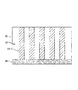
[0007] FIG. 1 illustrates a partial cross-sectional view of an exemplary
transducer structure that includes an array of a plurality of transducer
posts.
[0008] FIG. 2 is a flow chart of an exemplary method of manufacturing
an array of transducer posts used with the structure shown in FIG. 1.
[0009] FIG. 3A illustrates an exemplary slurry system that may be used
in manufacturing transducer posts used with the structure shown in FIG. 1.
[0010] FIG. 3B illustrates another process view of the slurry system
shown in FIG. 3A.
[0011] FIG. 4 illustrates an exemplary light modulating system that may
be used in manufacturing transducer posts used with the structure shown in
FIG. I.
[0012] FIG. 5A illustrates the light modulating system shown in FIG. 4
being used to fabricate an exemplary light pattern.
[0013] FIG. 5B illustrates another process view of the light modulating
system shown in FIG. 4.
3
CA 2790266 2017-07-07
249643
[0014] FIG. 5C illustrates another process view of the light modulating
system shown in FIG. 4.
[0015] FIG. 5D illustrates another process view of the light modulating
system shown in FIG. 4.
[0016] FIG. 6 illustrates a perspective view of the structure shown in
FIG. 1.
[0017] FIG. 7 illustrates a side view of exemplary transducer posts for
the structure shown in FIG. 6.
[0018] FIG. 8 illustrates another side view of exemplary transducer posts
that may be used with the structure shown in FIG. 6.
[0019] FIG. 9 illustrates a plan view of an exemplary array of transducer
posts that may be used with the structure shown in FIG. 6.
[0020] FIG. 10 illustrates a perspective view of the array of transducer
posts shown in FIG. 9.
[0021] FIG. 11 illustrates a partial side view of an exemplary probe
fabricated with an array of transducer posts.
DETAILED DESCRIPTION OF THE INVENTION
[0022] FIG. 1 illustrates a cross sectional view of an exemplary
transducer structure 10 that includes an array 12 of a plurality of transducer
posts 14
disposed on a substrate 16. FIG. 2 is a flow chart of an exemplary method 200
that may
be used to fabricate array 12 of transducer posts 14. In the exemplary
embodiment,
method 200 includes forming 202 a layer 18 (shown in FIG. 3) on substrate 16.
Substrate
16 may include materials such as, but not limited to, plastic, glass, mica,
metals,
ceramics, and/or combinations thereof. Layer 18 is fabricated from materials
such as, but
not limited to, an ultrasound transducer material, and a photo-curable,
polymer material.
4
CA 2790266 2017-07-07
249643
Ultrasound transducer material may include one or more conductive materials,
and/or one
or more piezoelectric materials and/or one or more acoustic materials.
[0023] In the exemplary embodiment, a plurality of selected regions of
layer 18 is exposed 204 to a programmable light system 30 (shown in FIG. 4).
Next,
selected regions of layer 18 are cured 206 to form polymerized ultrasound
transducer
regions and unexposed regions of layer 18 are selectively removed 208 to
create a desired
arrangement of polymerized ultrasound transducer posts 14. Method 200 also
includes
debinding 210 polymerized ultrasound transducer posts 14 to selectively remove
organic
polymers, and then sintering 212 the arrangement of polymerized ultrasound
transducer
posts 14 to obtain a desired array 12 of ultrasound transducer posts 14.
[0024] FIG. 3A illustrates an exemplary slurry system 20 that may be
used in preparing layer 18. FIG. 3B illustrates another process view of the
slurry system
shown in FIG. 3A. Any suitable manufacturing method for forming thin uniform
layers
may be used to form layer 18. In the exemplary embodiment, dispenser 24 of
slurry
system 20 deposits a bead 26 of slurry 22 on substrate 16, wherein slurry 22
includes the
transducer material and photopolymer material. A size of slurry bead 26 and/or
a rate of
bead 26 formation may be controlled based on predetermined characteristics of
structure
10. During manufacture, a blade 28 controllably wipes slurry 22 to facilitate
forming
layer 18 with desired sizing and shaping. Other suitable systems (not shown)
for use in
preparing layer 18 include, but are not limited to, a knife blade technique, a
doctor blade
technique, and screen printing known in the art.
[0025] In the exemplary embodiment, layer 18 includes piezoelectric
material 15 and photo-curable, polymer material 17. Any suitable piezoelectric
material
may be used in fabricating layer 18. For example, piezoelectric materials may
include,
but are not limited to only including, lead zirconate titanate, lead
metaniobate, lithium
niobate, bismuth titanate, lead titanate, and/or combinations thereof. Other
piezoelectric
materials may include, but are not limited to only including, lead magnesium
niobate,
lead zinc niobate, lead nickel niobate, bismuth scandium oxide, and/or
combinations
CA 2790266 2017-07-07
249643
thereof. In the exemplary embodiment, the piezoelectric material includes lead
zirconate
titanate (PZT). In another embodiment, layer 18 may also include any suitable
conductive material and a photopolymer. For example, a suitable conductive
material
may include, but is not limited to only including, platinum, palladium,
platinum-
palladium alloys, and/or combinations thereof. Any photo-curable polymer that
is
compatible with the one or more ultrasound transducer materials used to form
layer 18.
Further, any photo-curable material that polymerizes when exposed to a light
of a given
wavelength distribution may be used to fabricate layer 18.
[0026] FIG. 4 illustrates an exemplary light modulator system 30 that
may be used in manufacturing an array 12 of transducer post 14 used with
structure 10.
FIGS. 5a-5d illustrate light modulating system shown in FIG. 4 being used to
fabricate an
exemplary light pattern. In an embodiment, a spatial light modulator 34 is
systematically
moved to expose layer 18, using a "step-and-scan" manufacturing technique.
During
manufacturing, a plurality of selected regions 19 of layer 18 are exposed 204
to light of
a predetermined intensity and wavelength distribution that is capable of
initiating a
polymerization process. System 30 includes a computer 32 that provides digital
control
signals to control the modulating light intensity and/or direction of spatial
light modulator
34 to facilitate generating a predetermined light pattern 36 on layer 18. In
one
embodiment, programmable light pattern 36 is digitally controlled. Computer 32
generates electronic control signals and spatial light modulator 34 projects
predetermined
light pattern 36 on the plurality of selected regions 19 of layer 18 to expose
and to cure
206 those selected regions 19 of layer 18. Each layer 18 is exposed to the
digitally,
programmable light pattern 36, and the imaging of individual features is
dynamically
achieved via computer control. A digital pattern 38 representing the cross-
section of the
structure to be fabricated is projected onto layer 18. Spatial light modulator
34 selectively
cures 206 the photopolymer present within the selected region 19 of layer 18
to yield
polymerized regions within layer 18.
[0027] As best seen in FIGS. 5A-5D, during manufacture spatial light
modulator module 34 is movable in a generally horizontal plane along the X-
and Y-
6
CA 2790266 2017-07-07
CA 02790266 2012-09-13
249643
planes to emit the digitally programmable light pattern 36 in a desired
exposure pattern
42 on layer 18. Spatial light modulator module 34 may also be movable along
the Z-
plane. For example, spatial light modulator module 34 may be translated along
the X-
plane to produce a first exposure pattern 44 over at least a portion of layer
18, and
translated along the Y-plane to produce a different exposure pattern 46 on at
least a
portion of layer 18. Similarly, spatial light modulator 34 may be translated
along the Z-
plane to produce yet another exposure pattern 48 on at least a portion of
layer 18. The use
of this step-and-scan technique facilitates larger portions being fabricated
using small
area, high resolution, and digital masks.
[0028] Method 200 continues to selectively remove 208 unexposed
regions 21 of layer 18 to produce a desired arrangement of polymerized
transducer posts
14. Next, array 12 of polymerized transducer posts 14 is debinded 210 to
remove organic
polymers. Finally, in the exemplary embodiment, method 200 includes sintering
212
polymerized transducer posts 14 to obtain desired array 12 of ultrasound
transducer posts
14 spaced across substrate 16 (as shown in FIG. 1). Transducer posts 14 can be
placed at
any controlled spacing and/or can be fabricated independently with different
physical
dimensions and/or different shapes. Transducer posts 14 can be controllably
formed at
reduced costs with any spacing and/or have any physical dimensions and/or
shapes for
free-form, three dimensional formation that enables structure 10 to function
as described
herein.
[0029] The controllable formation and arrangement of transducer posts
14 facilitates enhanced resolution by a probe (such as probe 50 shown in FIG.
11) by
minimizing or substantially eliminating shear waves of ultrasound transducer
wavelengths traveling within array 12. Transducer posts 14 may have any
suitable
configuration, and/or orientation and/or sizing that facilitate minimizing or
eliminating
shear waves within array 12; that facilitates maintaining and/or enhancing
longitudinal
waves within array 12 and/or that facilitates enhancing resolution by probe
50.
7
CA 02790266 2012-09-13
249643
[0030] In an embodiment, plurality of transducer posts 14 are
controllably formed and arranged on substrate 16. The plurality of transducer
posts 14
are formed having a plurality of spatial positions located on the X-Y plane of
substrate
16. Further, the plurality of transducer posts 14 are formed having a
plurality of shapes
defined in the X-Y-Z plane of substrate 16. The plurality of spatial positions
and the
plurality of shapes of transducer posts 14 are configured to facilitate
minimizing shear
waves and maintaining longitudinal waves within array 12. In an embodiment,
spatial
positions and/or shapes of transducer posts 14 are configured to facilitate
interference
and/or cancellation of shear waves generated by posts 14 and traveling within
or among
posts 14. In the exemplary embodiment, spatial positions and/or shapes of
transducer
posts 14 further facilitate reducing amplitude of shear waves traveling within
or among
posts 14. The plurality of spatial positions and shapes facilitate enhancing
piezoelectric
properties and acoustic properties of a probe, such as probe 50 (shown in FIG.
11).
[0031] FIG. 6 illustrates a perspective view of structure 10 including
controllably formed and arranged array 12 of transducer posts 14. In an
embodiment, the
plurality of spatial positions of transducer posts 14 includes a periodic
arrangement of the
plurality of transducer posts 14 on substrate 16. Alternatively, the plurality
of spatial
positions of transducer posts 14 includes an aperiodie arrangement of the
plurality of
transducer posts 14 on substrate 16. In an embodiment, the plurality of
spatial positions
of transducer posts 14 located on substrate 16 includes at least one of a 0-3,
3-0, 1-3, 3-1,
3-3 and 2-2 composite structure.
100321 In the exemplary embodiment, transducer posts 14 are positioned
such that a spacing 52 is defined between adjacent transducer posts 14. In an
embodiment, spacing 52 is equidistant among at least one of the transducer
posts 14 and
adjacent transducer posts 14. In another embodiment, spacing 52 is non-
equidistant
among at least one of the transducer posts 14 and adjacent transducer posts
14. In one
embodiment, spacing 52 between transducer posts 14 is between about 5 microns
to
about 50 microns. Each transducer post 14 includes a proximal end 54, a distal
end 56,
and a body 58 that extends there between. Proximal end 54 is coupled to
substrate 16,
8
CA 02790266 2012-09-13
249643
and body 58 extends from proximal end 54 away from substrate 16. In the
exemplary
embodiment, at least one of the plurality of transducer posts 14 has a body 58
that is
formed with a substantially uniform configuration 60. More specifically, as
used herein,
uniform configuration 60 includes a substantially smooth side profile and/or a
substantially uniform patterned side profile (not shown) that accommodates
minor
variations in cross-sectional shape along body 58. Further, as used herein,
uniform
configuration 60 includes substantially similar cross sectional areas for
bodies 58.
[0033] In another embodiment, the plurality of shapes for the plurality of
transducer posts 14 includes a different cross sectional area for at least one
transducer
post 14 of the plurality transducer posts 14. Still further, in an embodiment,
the plurality
of shapes for the plurality of transducer posts 14 includes a different side
profile shape for
at least one transducer post 14 of the plurality of transducer posts 14.
[0034] In the exemplary embodiment, at least one body 58 of the
plurality of transducer posts 14 has a non-orthogonal shape 62 such as, but
not limited to,
a columnar shape including a substantially circular cross section. In one
embodiment, a
diameter 64 of such a transducer element 14 is between about 1 micron to about
50
microns in length. In the exemplary embodiment, bodies 58 each have a
substantially
equal height 66 as measured between ends 54 and 56. In the exemplary
embodiment,
each transducer element height 66 is between about 5 microns to about 150
microns.
Moreover, in the exemplary embodiment, body 58 includes a height to width
aspect ratio
of at least 2:1. Alternatively, at least one body 58 is formed with a
different height 66 as
compared to other bodies 58 in the plurality of transducer posts 14 within
array 12.
[0035] FIG. 7 illustrates a side view of exemplary transducer posts 14
for the structure shown in Fig. 6. In the exemplary embodiment, at least one
transducer
post 14 can have a different density 68 than other transducer posts 14 of the
plurality of
transducer posts 14. Alternatively, each transducer post 14 of the plurality
of transducer
posts 14 can have substantially similar densities. The density structure of
each transducer
post 14 facilitates minimizing or substantially eliminating shear waves of
ultrasonic
9
CA 02790266 2012-09-13
249643
transducer waves traveling within array 12. Transducer post 14 can be formed
with any
density distribution that facilitates eliminating shear waves from traveling
within, or
among posts 14 of array 12. Transducer post 14 can be formed with any density
distribution that facilitates maintaining longitudinal waves of waves
traveling within, or
among, posts 14 of array 12. Further, in an embodiment, each transducer post
14 of the
plurality of transducer posts 14 can have a uniform density distribution or a
non-uniform
density distribution. Transducer post 14 can also include structures such as,
but not
limited to, blind holes and thru-holes distributed within transducer post 14.
[0036] FIG. 8 illustrates a side view of an exemplary transducer element
14 formed with a non-orthogonal shape 70. In the exemplary embodiment,
transducer
element 14 is formed with a columnar shape that is defined by a hexagonal
cross section.
In the exemplary embodiment, a length 72 of each side 73 of transducer element
14 is
between about 1 micron to about 50 microns, and each transducer element 14 has
a height
74 as measured from substrate 16 of between about 5 microns to about 150
microns.
[0037] FIG. 9 illustrates a plan view of an exemplary array 76 of
transducer posts 14 disposed on substrate 16 shown in Fig. 6. FIG. 10
illustrates a
perspective view of array 76. In the exemplary embodiment, transducer posts 14
within
array 76 are formed with a non-orthogonal shape, such as, but not limited to,
a columnar
shape defined by a substantially circular cross section. Alternatively,
transducer posts 14
in array 76 can be formed with other non-orthogonal shapes (not shown) such
as, but not
limited to, hexagonal cross-sectional shapes. Moreover, transducer posts 14 in
array 76
may be formed with orthogonal shapes (not shown).
[0038] As shown, at least some transducer posts 14 are formed with
different physical sizing within array 76, as compared to other transducer
posts 14 within
array 76. More specifically, in the exemplary embodiment, array 76 includes a
plurality
of transducer posts 78 that are formed with a larger cross sectional size as
compared to
other transducer posts 84 in array 76. Moreover, in an embodiment, each
transducer
element 78 within array 76 has a larger diameter 80 than a diameter 82 of each
adjacent
CA 02790266 2012-09-13
249643
transducer element 84. In the exemplary embodiment, each diameter 80 is
approximately
30% to 50% larger than each diameter 82.
[0039] In array 76, each transducer element 78 is positioned between a
pair 79 of transducer posts 84 and a grouping 81 of other transducer posts 84.
Grouping
81 of transducer posts 84 may include a plurality of transducer posts 84. In
one
embodiment, grouping 81 includes four transducer posts 84. In the exemplary
embodiment, spacing 83 defined between adjacent transducer posts 84 is between
about 5
microns to about 50 microns. Further, spacing 85 defined between transducer
element 78
and each adjacent transducer element 84 is between about 5 microns to about 50
microns.
The orientation of array 76, and the shape and/or size of transducer posts 78
and 84
facilitate minimizing or substantially eliminating shear waves from traveling
within, or
among, transducer posts 14 of transducer structure 10. Further, the
orientation of array
76, and the shape and/or size of transducer posts 78 and 84 facilitate
maintaining
longitudinal waves traveling within, or among, transducer posts 14 of
transducer structure
10. Additionally, the orientation of array 76, and the shape and/or size of
transducer
posts 78 and 84 facilitate reducing an overall size of structure 10 to enable
probe, such as
probe 50 (shown in FIG. 11), to operate at higher frequencies than probes with
known
spacing and/or orientation and/or shapes. Further, the orientation of array
76, and the
shape and/or size of transducer posts 78 and 84 facilitate increasing the
resolution in
images obtained by probe 50.
[0040] FIG. 11 illustrates a partial side view of exemplary probe 50
fabricated with array 12 of transducer posts 14. Probe 50 includes array 12 of
transducer
posts 14 with electrodes 86 coupled on each top side 88 that enable probe 50
to be
electrically coupled to a power source (not shown). Posts 14 convert
electrical energy
into ultrasonic energy. Probe 50 also includes a filler 92 that circumscribes
the plurality
of transducer posts 14 on substrate 16. In the exemplary embodiment, filler 92
includes
an epoxy material that holds the transducer posts together and supports the
electrode
material between post 14, which creates a composite material with a lower
acoustic
impedance as compared to monolithic ceramic materials and higher coupling
factor. This
11
CA 02790266 2012-09-13
249643
formation allows for a more efficient acoustic coupling between the transducer
post 14
and the component (not shown) being inspected by probe 50.
[0041] As used herein, the term "controlled or arranged," when used in
the context of a discussion of one or more components of the structure and/or
transducer
post and/or probe, may refer to a physical geometry and/or a size and/or an
orientation of
the transducer posts as is independently user-defined or programmably
implemented. In
addition, the term may also refer to, and include the situation wherein the
arrangement of
the transducer posts of the probe is also user-defined, and may be, for
instance, non-
uniform and/or uniform. This arrangement could be aperiodic/random over
controlled or
uncontrolled distances. The term "post" when used in the context of a
discussion of one
or more components of the structure and/or transducer post and/or probe, may
refer to
any features of piezoelectric materials.
[0042] The embodiments described herein provide geometries and/or
orientations and/or spacings for transducer posts to facilitate minimizing
and/or
eliminating shear waves and maintaining longitudinal waves, which in turn,
enhances the
performance of the associated probe, as compared to the performance of probes
that
include known transducer posts. The embodiments described herein include non-
orthogonal column cross-sections in either the x-y, x-z, or y-z planes such
as, for
instance, circular and hexagonal. Non-orthogonal cross sections further
facilitate
minimizing or substantially eliminating shear waves that are generated by the
application
of an electrical potential across the structure. The embodiment described
herein further
provide the ability to produce free-form, three dimensional transducer posts
for improved
higher electromechanical coupling coefficients, improved acoustic impedance
match
between the transducer and the article being inspected, and improved resonance
characteristics using cost effective manufacturing.
[0043] The embodiments described herein provide a structure for use
with a transducer probe. The disclosed dimensional ranges include all sub
ranges there
between. The dimensional ranges for the transducer posts facilitate reducing
an overall
12
249643
size of the transducer element to enable the probe to be operated at higher
frequencies.
Additionally, the dimensional ranges for the transducer element facilitate
increasing
resolution in images obtained by probe.
[0044] A technical effect of the of the embodiments described herein
includes the controlled array of transducer posts which facilitates minimizing
or
eliminating shear waves traveling within array of transducer structure.
Another technical
effect of the array of transducer posts described herein facilitates reducing
the size of the
transducer element to facilitate operating the probe at higher frequencies. A
further
technical effect technical effect of the array of transducer posts facilitates
increasing
resolution in images obtained by probe.
[0045] Exemplary embodiments of a transducer post, probe, and
methods of manufacturing the transducer post, structure, and probe and
assembling the
probe are described above in detail. The transducer post, structure, probe,
and methods
are not limited to the specific embodiments described herein, but rather,
components of
the transducer post and/or the probe and/or steps of the method may be
utilized
independently and separately from other components and/or steps described
herein. For
example, the probe and methods may also be used in combination with other
diagnostic
systems and methods, and are not limited to practice with only the ultrasonic
transducer
probe as described herein. Rather, the exemplary embodiments can be
implemented and
utilized in connection with many other diagnostic systems or other support
structures.
[0046] Although specific features of various embodiments of the
invention may be shown in some drawings and not in others, this is for
convenience only.
In accordance with the principles of the invention, any feature of a drawing
may be
referenced and/or claimed in combination with any feature of any other
drawing.
[0047] This written description uses examples to disclose the invention,
including the best wave, and also to enable any person skilled in the art to
practice the
invention, including making and using any layers or systems and performing any
incorporated methods. The patentable scope of the invention may include other
examples
13
CA 2790266 2017-07-07
249643
that occur to those skilled in the art in view of the description. Such other
examples are
intended to be within the scope of the invention.
14
CA 2790266 2017-07-07