Note: Descriptions are shown in the official language in which they were submitted.
CA 02790794 2014-06-09
54106-1185
- 1 -
Accelerator for charged particles
FIELD OF INVENTION
The invention relates to an accelerator for charged particles,
with a capacitor stack of electrodes concentrically arranged
with respect to one another, as used, in particular, in the
generation of electromagnetic radiation.
BACKGROUND
Particle accelerators serve to accelerate charged particles to
high energies. In addition to their importance in fundamental
research, particle accelerators are becoming ever more
important in medicine and for many industrial purposes.
Until now, linear accelerators and cyclotrons were used to
produce a particle beam in the MV range, these usually being
very complicated and complex instruments.
Such accelerators are used in free-electron lasers (FEL). A
fast electron beam accelerated by the accelerator is subjected
to periodic deflection in order to generate synchrotron
radiation.
Such accelerators can also be used in the case of X-ray
sources, in which X-ray radiation is generated by virtue of a
laser beam interacting with a relativistic electron beam, as a
result of which X-ray radiation is emitted as a result of
inverse Compton scattering.
Another type of known particle accelerators are so-called
electrostatic particle accelerators with a DC high-voltage
source. Here, the particles to be accelerated are exposed to a
static electric field.
By way of example, cascade accelerators (also Cockcroft-Walton
accelerators) are known, in which a high DC
CA 02790794 2014-06-09
54106-1185
- 2 -
=
voltage is generated by multiplying and rectifying an AC
voltage by means of a Greinacber circuit, which is connected a
number of times in series (cascaded), and hence a strong
electric field is provided.
SUMMARY
Some embodiments of the invention are based on the object of specifying
an accelerator for accelerating charged particles, which, while
having a compact design, enables particularly efficient
particle acceleration to high particle energies and which, as
a result thereof, can be used for generating electromagnetic
radiation.
The accelerator according to some embodiments of the invention for
accelerating charged particles comprise:
a capacitor stack
- with a first electrode, which can be brought to a first
potential,
- with a second electrode, which is concentrically arranged
with respect to the first electrode and can be brOught to a
second potential that differs from the first potential,
- with at least one intermediate electrode, which is
concentrically arranged between the first electrode and the
second electrode and which can be brought to an intermediate
potential situated between the first potential and the
second potential.
There is a switching device, to which the electrodes of the
capacitor stack - i.e. the first electrode, the second
electrode and the intermediate electrodes - are connected and
which is embodied such that, during operation of the switching
device, the electrodes of the capacitor 6-tack concentrically
arranged with respect to one another are brought to increasing
CA 02790794 2012-08-22
PCT/EP2011/051462 - 2a -
2010P01981WOUS
potential levels.
A first acceleration channel is present, which is formed by
first openings in the electrodes of the capacitor stack
CA 02790794 2012-08-22
PCT/EP2011/051462 - 3 -
2010P01981W0US
such that charged particles can be accelerated by the
electrodes along the first acceleration channel. A second
acceleration channel is also present, which is formed by
second openings in the electrodes of the capacitor stack such
that charged particles can be accelerated along the second
acceleration channel by the electrodes.
Furthermore, a device is present, by means of which the
accelerated particle beam is influenced in the interior of the
capacitor stack, as a result of which photons that are emitted
by the particle beam are generated. As a result of the device,
an interaction with the accelerated particle beam is created,
which interaction changes the energy, the speed and/or the
direction of propagation. As a result of this, the
electromagnetic radiation, more particularly coherent
electromagnetic radiation, which emanates from the particle
beam can be produced.
The capacitor stack can more particularly comprise a plurality
of intermediate electrodes concentrically arranged with
respect to one another, which are connected by the switching
device such that, when the switching device is in operation,
the intermediate electrodes are brought to a sequence of
increasing potential levels between the first potential and
the second potential. The potential levels of the electrodes
of the capacitor stack increase in accordance with the
sequence of their concentric arrangement. Here, the high-
voltage electrode can be the innermost electrode in the case
of the concentric arrangement, whereas the outermost electrode
can be e.g. a ground electrode. An accelerating potential is
formed between the first and second electrode.
Thus, the capacitor stack and the switching device constitute a
DC high-voltage source because the central electrode can be
brought to a high potential. The potential difference provided
by the high-voltage source enables the device to be operated as
CA 02790794 2012-08-22
PCT/EP2011/051462 - 4 -
2010P01981W0US
an accelerator. The electric potential energy is converted into
kinetic energy of the particles by virtue of applying the high
potential between particle source and target. Two rows of holes
bore through the concentric electrode stack.
Charged particles are provided by a source and accelerated
through the first acceleration channel toward the central
electrode. Subsequently, after interaction with the device in
the center of the capacitor stack, e.g. within the innermost
electrode, the charged particles are routed away from the
central electrode through the second acceleration channel and
can once again reach the outside. As a result of deceleration
of the beam in the electric field, the energy expended for the
acceleration is recuperated, and so very large beam currents
and hence a great luminance can be obtained compared to the
applied electric power.
Overall, it is possible to achieve a particle energy in the MV
range in the case of a compact design and to provide a
continuous beam. A source substantially situated at ground
potential can for example provide negatively charged
particles, which are injected as particle beam and are
accelerated toward the central electrode through the first
acceleration channel.
Overall, the concentric arrangement enables a compact design
and, in the process, an expedient form for insulating the
central electrode.
For expedient use of the insulation volume, i.e. the volume
between the inner and the outer electrode, one or more
concentric intermediate electrodes are brought to suitable
potentials. The potential levels successively increase and can
be selected such that this results in a largely uniform field
strength in the interior of the entire insulation volume.
CA 02790794 2012-08-22
PCT/EP2011/051462 - 5 -
2010P01981W0US
The introduced intermediate electrode(s) moreover increase the
dielectric strength limit, and so higher DC voltages can be
produced than without intermediate electrodes. This is due to
the fact that the dielectric strength in a vacuum is
approximately inversely proportional to the square root of the
electrode spacings. The introduced intermediate electrode(s),
by means of which the electric field in the interior of the DC
high-voltage source becomes more uniform, at the same time
contribute to an advantageous increase in the possible,
attainable field strength.
In one embodiment, the device is embodied to provide a laser
beam, which interacts with the accelerated particle beam such
that the emitted photons emerge from inverse Compton
scattering of the laser beam at the charged particles of the
accelerated particle beam. The emitted photons are coherent.
The laser beam can advantageously be obtained by forming a
focus within the laser cavity.
The energy of the laser beam, the acceleration of the
particles and/or the type of particles can be tuned to one
another such that the emitted photons lie in the X-ray
spectrum. The accelerator can thus be operated as compact
coherent X-ray source.
The particle beam can be an electron beam. To this end, an
electron source can be arranged e.g. outside of the outermost
electrode of the capacitor stack.
In another embodiment, the device is embodied to generate a
transverse magnetic field, e.g. using a dipole magnet, with
respect to the direction of propagation of the particle beam.
This brings about a deflection of the accelerated particle
beam such that the photons are emitted from the particle beam
as synchrotron radiation. As a result of this, the accelerator
can as synchrotron radiation source and, more particularly, as
CA 02790794 2012-08-22
PCT/EP2011/051462 - 6 -
2010P01981WOUS
free-electron laser by coherent superposition of the
individual radiation lobes.
The device can, in particular, create a transverse magnetic
field which brings about a periodic deflection of the
accelerated particle beam along a path in the interior of the
capacitor stack, for example by a series of dipole magnets. As
a result of this, the accelerator can create coherent photons
particularly efficiently.
The electromagnetic radiation emitted by the particle beam can
emerge by means of a channel through the electrode stack.
In an advantageous embodiment, the electrodes of the capacitor
stack are insulated from one another by vacuum insulation. As
a result of this, it is possible to achieve insulation of the
high-voltage electrode which is as efficient, i.e. as space-
saving and robust, as possible. It follows that there is a
high vacuum in the insulation volume. A use of insulating
materials would be disadvantageous in that the materials tend
to agglomerate internal charges
- which, in particular, are caused by ionizing radiation
during operation of the accelerator - when exposed to an
electric DC field. The agglomerated, traveling charges cause a
very inhomogeneous electric field strength in all physical
insulators, which then leads to the breakdown limit being
exceeded locally and hence to the formation of spark channels.
Insulation by a high vacuum avoids such disadvantages. The
electric field strength that can be used during stable
operation can be increased thereby. As a result of this, the
arrangement is substantially free from insulator materials -
except for a few components such as e.g. the electrode mount.
In the case of an accelerator, the use of a vacuum is moreover
advantageous in that there is no need to provide a separate
beam tube, which in turn at least in part has an insulator
CA 02790794 2012-08-22
PCT/EP2011/051462 - 6a -
2010P01981WOUS
surface. This also prevents critical
CA 02790794 2012-08-22
PCT/EP2011/051462 - 7 -
2010P01981WOUS
problems of the wall discharge from occurring along the
insulator surfaces because the acceleration channel now no
longer needs to have insulator surfaces. An acceleration
channel is merely formed by openings in the electrodes which
are situated in a line, one behind the other.
In one advantageous embodiment, the switching device comprises
a high-voltage cascade, more particularly a Greinacher cascade
or a Cockcroft-Walton cascade. By means of such a device, it
is possible to charge the first electrode, the second
electrode and the intermediate electrodes for generating the
DC voltage by means of a comparatively low AC voltage. This
embodiment is based on the concept of a high-voltage
generation, as is made possible, for example, by a Greinacher
rectifier cascade.
In one embodiment variant, the capacitor stack is subdivided
into two mutually separate capacitor chains by a gap which
runs through the electrodes. As a result of separating the
concentric electrodes of the capacitor stack into two mutually
separate capacitor chains, the two capacitor chains can
advanfageously be used for forming a cascaded switching device
such as a Greinacher cascade or Cockcroft-Walton cascade.
Here, each capacitor chain constitutes an arrangement of
(partial) electrodes which, in turn, are concentrically
arranged with respect to one another.
In an embodiment of the electrode stack as spherical shell
stack, the separation can be brought about by e.g. a cut along
the equator, which then leads to two hemispherical stacks.
In the case of suCh a circuit, the individual capacitors of
the chains can be respectively charged to the peak-peak
voltage of the primary input AC voltage which serves to charge
the high-voltage source. The aforementioned potential
equilibration, a uniform electric field distribution
CA 02790794 2014-06-09
54106-1185
- 8 -
and hence an optimal use of the insulation clearance can be
achieved in a simple manner.
In an advantageous fashion, the switching device, which
comprises a high-voltage cascade, can interconnect the two
mutually separated capacitor chains and, in particular, be
arranged in the gap. The input AC voltage for the high-voltage
cascade can be applied between the two outermost electrodes of
= the capacitor chains because, =for example, these Can be
accessible from the outside. The diode chains of a rectifier.
circuit can then be applied in the equatorial gap - and hence
in a space-saving manner.
The electrodes of the capacitor stack can be formed such that
they are situated on the surface of an ellipsoid, more
particularly on the surface of a sphere, or on the surface of
a cylinder. These shapes are physically expedient. Selecting
the shape of the electrodes as in the case of a hollow sphere
or the sphericalcapacitor is particularly expedient.. Similar
shapes such as e.g. in the case of a cylinder are also
possible, wherein the latter however usually has a
comparatively inhomogeneous electric field distribution.
The low inductance of the shell-like potential electrodes
allows the application of high operating frequencies, and so
the voltage reduction during the current drain remains
= restricted despite relatively low = capacitance of the
individual capacitors.
CA 02790794 2014-06-09
54106-1185
- 8a -
According to one aspect of the present invention, there is
provided an accelerator for accelerating charged particles,
comprising: a capacitor stack comprising: a first electrode
configured to be brought to a first potential, a second
electrode concentrically arranged with respect to the first
electrode and which is configured to be brought to a second
potential that differs from the first potential, and at least
one intermediate electrode concentrically arranged between the
first electrode and the second electrode and which is
configured to be brought to an intermediate potential between
the first potential and the second potential, a switching
device to which the electrodes of the capacitor stack are
connected, the switching device being configured such that,
during operation of the switching device, the electrodes of the
capacitor stack concentrically arranged with respect to one
another can be brought to increasing potential levels, a first
acceleration channel formed by first openings in the electrodes
of the capacitor stack such that charged particles can be
accelerated by the electrodes along the first acceleration
channel, a second acceleration channel formed by second
openings in the electrodes of the capacitor stack such that
charged particles can be accelerated by the electrodes along
the second acceleration channel, and a device configured to
influence the accelerated particle beam in the interior of the
capacitor stack, as a result of which photons that are emitted
by the particle beam are created.
According to another aspect of the present invention, there is
provided a method for accelerating charged particles,
comprising: providing a capacitor stack comprising: a first
electrode configured to be brought to a first potential, a
ak 02790794 2014-06-09
54106-1185
- 8b -
second electrode concentrically arranged with respect to the
first electrode and which is configured to be brought to a
second potential that differs from the first potential, and at
least one intermediate electrode concentrically arranged
between the first electrode and the second electrode and which
is configured to be brought to an intermediate potential
between the first potential and the second potential,
controlling a switching device to bring the capacitor stack
concentrically arranged with respect to one another to
increasing potential levels, accelerating charged particles by
electrodes along a first acceleration channel formed by first
openings in the electrodes of the capacitor stack, accelerating
charged particles by electrodes along a second acceleration
channel formed by second openings in the electrodes of the
capacitor stack, and using a device to influence the
accelerated particle beam in the interior of the capacitor
stack, as a result of which photons that are emitted by the
particle beam are created.
BRIEF DESCRIPTION OF THE DRAWINGS
Exemplary embodiments of the invention will be explained in
more detail on the basis of the following drawing, without
however being restricted thereto. In detail:
figure 1 shows a schematic illustration of a Greinacher
circuit, as known from the prior art,
CA 02790794 2014-06-09
54106-1185
- 9 -
figure 2 shows a schematic illustration of a section through a
DC high-voltage source with a particle source in the
center,
figure 3 shows a schematic illustration of a section through a
DC high-voltage source according to figure 2, with an
electrode spacing decreasing toward the center,
figure 4 shows a schematic illustration of a section through a
DC high-voltage source which is embodied as free-
electron laser,
figure 5 shows a schematic illustration of a section through a
DC high-voltage source which is embodied as coherent
X-ray source,
figure 6 shows a schematic illustration of the electrode design
with a stack of cylindrically arranged electrodes,
figure 7 shows an illustration of the diodes of the switching
device, which diodes are embodied as vacuum-flask-free
electron tubes,
figure 8 shows a diagram showing the charging process as a
function of pump cycles, and
figure 9 shows the advantageous Kirchhoff-form of the electrode
ends.
DETAILED DESCRIPTION
In the figures, the same parts have been provided with the
same reference signs.
The principle of a high-voltage cascade 9, which is configured
as per a Greinacher circuit, should be clarified using the
circuit diagram in figure 1.
CA 02790794 2012-08-22
PCT/EP2011/051462 - 9a -
2010P01981WOUS
An AC voltage U is applied to an input 11. The first half-wave
charges the capacitor 15 to the voltage U
CA 02790794 2012-08-22
PCT/EP2011/051462 - 10 -
2010P01981W0US
via the diode 13. In the subsequent half-wave of the AC
voltage, the voltage U from the capacitor 13 is added to the
voltage U at the input 11, such that the capacitor 17 is now
charged to the voltage 2U via the diode 19. This process is
repeated in the subsequent diodes and capacitors, and so the
voltage 6U is obtained in total at the output 21 in the case
of the circuit shown in figure 1. Figure 2 also clearly shows
how, as a result of the illustrated circuit, the first set 23
of capacitors respectively forms a first capacitor chain and
the second set 25 of capacitors respectively forms a second
capacitor chain.
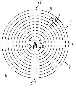
Figure 2 shows a schematic section through a high-voltage
source 31 with a central electrode 37, an outer electrode 39
and a row of intermediate electrodes 33, which are
interconnected by a high-voltage cascade 35, the principle of
which was explained in figure 1, and which can be charged by
this high-voltage cascade 35.
The electrodes 39, 37, 33 are embodied in the form of a hollow
sphere and arranged concentrically with respect to one
another. The maximum electric field strength that can be
applied is proportional to the curvature of the electrodes.
Therefore, a spherical shell geometry is particularly
expedient.
Situated in the center there is the high-voltage electrode 37;
the outermost electrode 39 can be a ground electrode. As a
result of an equatorial cut 47, the electrodes 37, 39, 33 are
subdivided into two mutually separate hemispherical stacks
which are separated by a gap. The first hemispherical stack
forms a first capacitor chain 41 and the second hemispherical
stack forms a second capacitor chain 43.
In the process, the voltage U of an AC voltage source 45 is
respectively applied to the outermost electrode shell halves
CA 02790794 2012-08-22
PCT/EP2011/051462 - 10a -
2010P01981W0US
39', 39". The diodes 49 for forming the circuit are arranged
in the region of the great circle of halves of the hollow
spheres, i.e. in the equatorial cut 47 of the respective
hollow spheres.
=
CA 02790794 2012-08-22
PCT/EP2011/051462 - 11 -
- 2010P01981WOUS
The diodes 49 form the cross-connections between the two
capacitor chains 41, 43, which correspond to the two sets 23,
25 of capacitors from figure 1.
In the case of the high-voltage source 31 illustrated here, an
acceleration channel 51, which runs from e.g. a particle
source 53 arranged in the interior and enables the particle
beam to be extracted, is routed through the second capacitor
chain 43. The particle stream of charged particles experiences
a high acceleration voltage from the hollow-sphere-shaped
high-voltage electrode 37.
The high-voltage source 31 or the particle accelerator is
advantageous in that the high-voltage generator and the
particle accelerator are integrated into one another because
in this case all electrodes and intermediate electrodes can be
housed in the smallest possible volume.
In order to insulate the high-voltage electrode 37, the whole
electrode arrangement is insulated by vacuum insulation. Inter
alia, this affords the possibility of generating particularly
high voltages of the high-voltage electrode 37, which results
in a particularly high particle energy. However, in principle,
insulating the high-voltage electrode by means of solid or
liquid insulation is also conceivable.
The use of vacuum as an insulator and the use of an
intermediate electrode spacing of the order of 1 cm affords
the possibility of achieving electric field strengths with
values of more than 20 MV/m. Moreover, the use of a vacuum is
advantageous in that the accelerator need not operate at low
load during operation due to the radiation occurring during
the acceleration possibly leading to problems in insulator
materials. This allows the design of smaller and more compact
machines.
CA 02790794 2012-08-22
PCT/EP2011/051462 - ha -
2010P01981WOUS
Figure 3 shows a development of the high-voltage source shown
in figure 2, in which the spacing of the electrodes 39, 37,
CA 02790794 2012-08-22
PCT/EP2011/051462 - 12 -
2010P01981W0US
33 decreases toward the center. As a result of such an
embodiment, it is possible to compensate for the decrease of
the pump AC voltage, applied to the outermost electrode 39,
toward the center such that a substantially identical field
strength nevertheless prevails between adjacent electrode
pairs. As a result of this, it is possible to achieve a
largely constant field strength along the acceleration channel
51. This embodiment can likewise be applied to the
applications and embodiments explained below.
Figure 4 shows a development of the high-voltage source shown
in figure 2 as a free-electron laser 61. The circuit device 35
from figure 2 is not illustrated for reasons of clarity, but
is identical in the case of the high-voltage source shown in
figure 4. The design can likewise have an electrode spacing
which decreases toward the center, as shown in figure 3.
In the example illustrated here, the first capacitor chain 41
also has an acceleration channel 53 which is routed through
the electrodes 33, 37, 39.
In place of the particle source, a magnet device 55 is arranged
in the interior of the central high-voltage electrode 37 and it
can be used to deflect the particle beam periodically. It is
then possible to produce electrons outside of the high-voltage
source 61, which electrons are accelerated through the first
capacitor chain 41 toward the central high-voltage electrode 37
along the acceleration channel 53. Coherent synchrotron
radiation 57 is created when passing through the magnet device
55 and the accelerator can be operated as a free-electron laser
61. The electron beam is decelerated again by the acceleration
channel 51 of the second capacitor chain 43 and the energy
expended for acceleration can be recuperated.
The outermost spherical shell 39 can remain largely closed and
thus assume the function of a grounded housing.
CA 02790794 2012-08-22
PCT/EP2011/051462 - 13 -
2010P01981W0US
The hemispherical shell situated directly therebelow can then
be the capacitor of an LC resonant circuit and part of the
drive connector of the switching device.
For such a type of acceleration, the accelerator can provide a
MV high-voltage source with N = 50 levels, i.e. a total of
100 diodes and capacitors. In the case of an inner radius of r
- 0.05 m and a vacuum insulation with a dielectric strength of
MV/m, the outer radius is 0.55 m. In each hemisphere there
are 50 intermediate spaces with a spacing of 1 cm between
adjacent spherical shells.
A smaller number of levels reduces the number of charge cycles
_
and the effective internal source impedance, but increases the
demands made on the pump charge voltage.
The diodes arranged in the equatorial gap, which interconnect
the two hemisphere stacks can, for example, be arranged in a
spiral-like pattern. According to equation (3.4), the total
capacitance can be 74 pF and the stored energy can be 3.7 kJ.
A charge current of 2 mA requires an operating frequency of
approximately 100 kHz.
Figure 5 shows a development of the accelerator, shown in
figure 4, for of a source 61' for coherent X-ray radiation.
In place of the particle source, a laser device 59 is arranged in
the interior of the central high-voltage electrode 37 and it can
be used to generate a laser beam 58 and direct the latter onto
the particle beam. As a result of interaction with the particle
beam, photons 57' are created as a result of inverse Compton
scattering, which photons are emitted by the particle beam.
Figure 6 illustrates an electrode form in which hollow-cylinder-
shaped electrodes 33, 37, 39 are arranged concentrically with
respect to one another. A gap divides the electrode stack into
CA 02790794 2012-08-22
PCT/EP2011/051462 - 14 -
2010P01981WOUS
two mutually separate capacitor chains, which can be connected
by a switching device with a configuration analogous to the
one in figure 2.
Figure 7 shows a shown embodiment of the diodes of the
switching device. The concentrically arranged, hemisphere-
shell-like electrodes 39, 37, 33 are only indicated in the
illustration for reasons of clarity.
In this case, the diodes are shown as electron tubes 63, with
a cathode 65 and an anode 67 opposite thereto. Since the
switching device is arranged within the vacuum insulation, the
vacuum flask of the electron tubes, which would otherwise be
required for operating the electrodes, can be dispensed with.
The electron tubes 63 can be controlled by thermal heating or
by light.
In the following text, more detailed explanations will be
offered in respect of components of the high-voltage source or
in respect of the particle accelerator.
Spherical capacitor
The arrangement follows the principle shown in figure 1 of
arranging the high-voltage electrode in the interior of the
accelerator and the concentric ground electrode on the outside
of the accelerator.
A spherical capacitor with an inner radius r and an outer
radius R has a capacitance given by
r R
C vg 47rfo (3.1)
R r
The field strength at a radius p is then given by
(3.2)
=
CA 02790794 2012-08-22
PCT/EP2011/051462 - 14a -
2010P01981WOUS
E= _______________________________ rR (3.2)
(R -r)p
CA 02790794 2012-08-22
PCT/EP2011/051462 - 15 -
2010P01981WOUS
This field strength has a quadratic dependence on the radius
and therefore increases strongly toward the inner electrode.
At the inner electrode surface p = r, the maximum
r(R r)U (3.3)
has been attained. This is disadvantageous from the point of
view of the dielectric strength.
A hypothetical spherical capacitor with a homogeneous electric
field would have the following capacitance:
R2 rR 4-
e. "! = 4.7reo (3.4)
R r
As a result of the fact that the electrodes of the capacitors
of the Greinacher cascade have been inserted as intermediate
electrodes at a clearly defined potential in the cascade
accelerator, the field strength distribution is linearly
fitted over the radius because, for thin-walled hollow
spheres, the electric field strength approximately equals the
flat case
¨ r)
with minimal maximum field strength.
The capacitance between two adjacent intermediate electrodes
is given by
rkr-k_t
Ck itXfi) ________________________________
rvit
Hemispherical electrodes and equal electrode spacing d = (R-r)/N
CA 02790794 2012-08-22
PCT/EP2011/051462 - 15a -
2010P01981W0US
leads to rk= r +kd and to the following electrode capacitances:
r-2 rd (2rd d2) k
CA 02790794 2012-08-22
PCT/EP2011/051462 - 16 -
2010P01981WOUS
Rectifier
Modern soft avalanche semiconductor diodes have very low
parasitic capacitances and have short recovery times. A
connection in series requires no resistors for equilibrating
the potential. The operating frequency can be selected to be
comparatively high in order to use the relatively small inter-
electrode capacitances of the two Greinacher capacitor stacks.
In the case of a pump voltage for charging the Greinacher
cascade, it is possible to use a voltage of U1rc,4100kV, i.e. 70
kVeff. The diodes must withstand voltages of 200 kV. This can
be achieved by virtue of the fact that use is made of chains
of diodes with a lower tolerance. By way of example, use can
be made of ten 20 kV diodes. By way of example, diodes can be
BY724 diodes by Philips, 3R757-200A diodes by EDAL or
ESJA5320A diodes by Fuji.
Fast reverse recovery times, e.g. trr100 ns for BY724,
minimize losses. The dimensions of the BY724 diode of 2.5 mm x
12.5 mm make it possible to house all 1000 diodes for the
switching device in a single equatorial plane for the
spherical tandem accelerator specified in more detail below.
In place of solid-state diodes, it is also possible to use
electron tubes in which the electron emission is used for
rectification. The chain of diodes can be formed by a
multiplicity of electrodes, arranged in a mesh-like fashion
with respect to one another, of the electron tubes, which are
connected to the hemispherical shells. Each electrode acts as
a cathode on one hand and as an anode on the other hand.
Discrete capacitor stack
The central concept consists of cutting through the
electrodes,
CA 02790794 2012-08-22
PCT/EP2011/051462 - 17 -
2010P01981W0US
which are concentrically arranged in succession, on an
equatorial plane. The two resultant electrode stacks
constitute the cascade capacitors. All that is required is to
connect the chain of diodes to opposing electrodes over the
plane of the cut. It should be noted that the rectifier
automatically stabilizes the potential differences of the
successively arranged electrodes to approximately 2 Uin, which
suggests constant electrode spacings. The drive voltage is
applied between the two outer hemispheres.
Ideal capacitance distribution
If the circuit only contains the capacitors from figure 3, the
stationary operation supplies an operating frequency f, a
charge
OtSf
I '
per full wave in the load through the capacitor Co. Each of the
capacitor pairs C2k and C2k+1 therefore transmits a charge
(k+1)Q.
The charge pump represents a generator-source impedance
v-4 , "," = . -
(1)
*f
k10.
As a result, a load current Iout reduces the DC output voltage
as pet
Coat 2.10In iktut 0.10)
CA 02790794 2012-08-22
PCT/EP2011/051462 - 18 -
2010P01981W0US
The load current causes a residual AC ripple at the DC output
with the peak-to-peak value of
tut I
(14.1
-
If all capacitors are equal to Ck = C, the effective source
impedance is
It, N34-0:0 N
mr-
412)
fC
and the peak-to-peak value of the AC ripple becomes
1-1
it; rs. 1 ____
a 3,
"
For a given total-energy store within the rectifier, a
capacitive inequality slightly reduces the values RG and RR
compared to the conventional selection of identical capacitors
in favor of the low-voltage part.
Figure 7 shows the. charging of an uncharged cascade of N = 50
concentric hemispheres, plotted over the number of pump
cycles.
Leakage capacitances
Any Charge exchange between the two columns reduces the
efficiency of the multiplier circuit, see figure 1, e.g. as a
result of the leakage capacitances cj and the reverse recovery
charge losses qj by the diodes D.
CA 02790794 2012-08-22
PCT/EP2011/051462 - 19 -
2010P01981WOUS
The basic equations for the capacitor voltages 131, at the
positive and negative extrema of the peak drive voltage U,
with the diode forward vOltage drop being ignored, are:
f,t7i = 14241-4 (314)
1i# 415)
lok,
tjr.;44
up to the index 2N - 2 and
r,=:+
tAtly... V2At - (118)
t-7:27y. wig.)
Using this nomenclature, the mean amplitude of the DC output
voltage is
(12f))
(los E
The peak-to-peak value of the ripple in the DC voltage is
2.4'171
:_=t Et,wit+ ilk .µ 420
With leakage capacitances ci parallel to the diodes Di, the
basic equations for the variables are u1 - 0, 132N - 2 U, and
the tridiagonal system of equations is
{ Yktven
+.00itk (Ok cglik =
I 0 VI
Reverse recovery charges
CA 02790794 2012-08-22
PCT/EP2011/051462 - 20 -
2010P01981WOUS
Finite reverse recovery times trr of the delimited diodes cause
a charge loss of
10= QD (12:0
with ri = f tr, and QD for the charge per full wave in the
forward direction. Equation (3.22) then becomes:
+ I Q YkOeti
0µ`-"000:k 41-7AA'r:141:4.1,41. 1 yk odd
(124)
Continuous capacitor stack
Capacitive transmission line
In Greinacher cascades, the rectifier diodes substantially
take up the AC voltage, convert it into DC voltage and
accumulate the latter to a high DC output voltage. The AC
voltage is routed to the high-voltage electrode by the two
capacitor columns and damped by the rectifier currents and
leakage capacitances between the two columns.
For a large number N of levels, this discrete structure can be
approximated by a continuous transmission-line structure.
For the AC voltage, the capacitor design constitutes a
longitudinal impedance with a length-specific impedance 3.
Leakage capacitances between the two columns introduce a
length-specific shunt admittance V. The voltage stacking of
the rectifier diodes brings about an additional specific
current load 3, which is proportional to the DC load current
CA 02790794 2012-08-22
PCT/EP2011/051462 - 21 -
2010P01981WOUS
'out and to the density of the taps along the tranSmission
line.
The basic equations for the AC voltage U(x) between the
columns and the AC direct-axis current I(X) are
U-r 0.20
U' 3 f126)
The general equation is an extended telegraph equation:
3!
tpt 37:1 =3J
1
In general, the peak-to-peak ripple at the DC output equals
the difference of the AC voltage amplitude at both ends of the
transmission line.
t;= U(t) Utti) (3.24)
Two boundary conditions are required for a unique solution to
this second-order differential equation.
One of the boundary conditions can be U (xd = Uin, given by
the AC drive voltage between the DC low-voltage ends of the
two columns. The other natural boundary condition determines
the AC current at the DC high-voltage end x = xl. The boundary
condition for a concentrated terminal AC impedance Zl between
the columns is:
014 ) '11:111 tltr
õ r¨ =.7
Li
In the unloaded case Zl = the
boundary condition is U' (x1) = 0.
,
CA 02790794 2012-08-22
PCT/EP2011/051462 - 22 -
2010P01981WOUS
Constant electrode spacing
For a constant electrode spacing t, the specific load current
is
,
õ.s V 160
1
and so the distribution of the AC voltage is regulated by
31 =
The average DC output voltage then is
I
µ,.
Eta* (322)
t 4
and the DC peak-to-peak ripple of the DC-voltage is
(3.M)
Optimal electrode spacing
The optimal electrode spacing ensures a constant electric DC
field strength 2 E in the case of the planned DC load current.
The specific AC load current along the transmission line,
depending on the position, is
3 - ________________________________________
The AC voltage follows from
CA 02790794 2012-08-22
PCT/EP2011/051462 - 23 -
2010P01981W0US
tar- 1141'=-3 too 1;134
0:
=
The electrode spacings emerge from the local AC voltage
amplitudes t(x) = U(x)/E.
The DC output voltage in the case of the planned DC load
current is Uout = 2Ed. A reduction in the load always increases
the voltages between the electrodes; hence operation with
little or no load can exceed the admissible E and the maximum
load capacity of the rectifier columns. It can therefore be
recommendable to optimize the design for unloaded operation.
For any given electrode distribution that differs from the one
in the configuration for a planned DC load current, the AC
voltage along the transmission line and hence the DC Output
voltage is regulated by equation (3.27).
Linear cascade_
In the case of a linear cascade with flat electrodes with the
width w, height h and a spacing s between the columns, the
transmission line impedances are
MO*
gbid, fuh.
4
Linear cascade - constant electrode spacing
The inhomogeneous telegraph equation is
0:47)
its t
,
CA 02790794 2012-08-22 ,
,
PCT/EP2011/051462 - 24 -
2010P01981W0US
Under the assumption of a line which extends from x = 0 to x -
d = Nt and is operated by Uin = U (0), and of a propagation
constant of y2 = 2/(h*s), the solution is
(
- OgIe4.- AxiSk"4 Ns
.
. 0:4 = '---- MR + __________________________________________________________
OA id . ,cos itlet
The diodes substantially tap the AC voltage, rectify it
immediately and accumulate it along the transmission line.
Hence, the average DC output voltage is
or - explicitly -
i
LitihNd /l Id s' 4\114
4toior-vir ______________________________ ,;--ttin + : oth -1,
1,, 14
A series expansion up to the third order in yd results in
tcAlt. -1. 24 '1.64 1 ,-. ---- = ', Li (M)
3 Iis r3. f ohm -
,
and
411-Ak -- .-.Vi it 4-= ;- - --,' .40:t . 4421
The load-current-related effects correspond to equation (3.12)
and (3.13).
Linear cascade - optimal electrode spacing
CA 02790794 2012-08-22
PCT/EP2011/051462 - 24a -
2010P01981W0US
In this case, the basic equation is
CA 02790794 2012-08-22
PCT/EP2011/051462 - 25 -
2010P01981WOUS
tL.2 E I s
172
14. ppm
It appears as if this differential equation has no closed
analytical solution. The implicit solution which satisfies
U'(0) = 0 is
cl4
(3441
titih V:_t (42 pm E jov
-ha - 1%01 ViVi
Radial cascade
Under the assumption of a stack of concentric cylinder
electrodes with a radius-independent height h and an axial gap
s between the columns as shown in figure 4, the radial-
specific impedances are
2iiretp,fr
- ___________________________ ,
(3.45)
etwrm
Radial cascade - constant electrode spacing
With an equidistant radial electrode spacing t = (R-r)/N, the
=basic equation
V'+
11$ p
has the general solution
RP) illtht/P) 4- BIG(114 __
4410 OAV?)
4-if (Die
, .
CA 02790794 2012-08-22
PCT/EP2011/051462 - 26 -
2010P01981WOUS
with y2 = 2/(h*s). Ko and I0 are the modified zeroth-order
Bessel functions and Lo is the modified zeroth-order STRUVE
function Lo .
The boundary conditions U' (r) = 0 at the inner radius r and U
(R) = Uin at the outer radius R determine the two constants
A
tri., ltf-A 4
- - I.4- TT{ frerYLoevit) - Tall) tlit. tiri 4- DI
. ,..... = = = . - , t-,pid .
4 '
1,41T)Kt.(49 littrriK60:1?)
ti
trift I( i Nr) 4 Irt 4 t 1K I (P0.)174i (IR) 4- Ko(!tri) {LI (ill 4. . .
4, " '
" OITY)
iR)Kthri --I.' ilKik.,R)
such that
= ioi''',AKI (;yr) 4- h 6 *)Robpi
00.) #
(7 MK 1. (ill ..1.- II frir)Ko6R)
. .
l'otit i . ,
:f... .4µ...õ.....õ.... , ..iovoi ..14.1
m¨,......L..:.:..-,,..:.,.;,¨,... .......:_' ,...L..`
= 40,04.41 :' ' =11:;'11
+11(7r)KOt';'1?)
- . 2 to(v)Ko(yRY- ..fdikiKii(107
"-- . Or) -f
,-- 7; = 14) ( ',, MK 1 NT) +1.teir)..(-;
R.);
)
131A)
K1 and Il are the modified Bessel functions and L1 is the
modified Struve function L1 = L'o - 2/n, all of first order.
The DC output voltage is
., 2 g . ._
.- f tili#0 .
(3.50
t i.; 'r, '
Radial cascade - optimal electrode spacing
- CA 02790794 2012-08-22
PCT/EP2011/051462 - 27 -
2010P01981W0US
The optimal local electrode spacing is t(p) = U(p)/E and the
basic equation becomes
I are _U2__ -(3:52)
r,:ut
1332)
p
It appears as if this differential equation has no closed
analytical solution, but it can be solved numerically.
Electrode shapes
Equipotential surfaces
A compact machine requires the dielectric field strength to be
maximized. Generally smooth surfaces with small curvature
should be selected for the capacitor electrodes. As a rough
approximation, the dielectric strength E scales with the
inverse square root of the electrode spacing, and so a large
number of closely spaced apart equipotential surfaces with
smaller voltage differences should be preferred over a few
large distances with large voltage differences.
Minimal E-field electrode edges
For a substantially planar electrode design with equidistant
spacing and a linear voltage distribution, the optimal edge-
shape is known as KIRCHHOFF form (see below),
A + WO I 1 + 2A cosl +
1-0 "in ____________
2tI 4r I -24 cos 0 A-
_ ¨ A2 ( 2.4"iut)
"2 Arrtgit - ;=irct'Aut
4$0.
2 ir . I
CA 02790794 2012-08-22
PCT/EP2011/051462 - 28 -
2010P01981WOUS
dependent on the parameters D D [0, n/2]. The electrode shape
is shown in figure 8. The electrodes have a normalized
distance of one and an asymptotic thickness 1 - A at a great
distance from the edge which, at the end face, tapers to a
vertical edge with the height
______________________________________ = (15)
7
The parameter 0 < A < 1 also represents the inverse E-field
overshoot as a result of the presence of the electrodes.
The thickness of the electrodes can be arbitrarily small
without introducing noticeable E-field distortions.
A negative curvature, e.g. at the openings along the beam
path, further reduces the E-field amplitude.
This positive result can be traced back to the fact that the
electrodes only cause local interference in an already
existing E-field.
The optimal shape for free-standing high-voltage electrodes is
ROGOWSKI- and BORDA profiles, with a peak value in the E-field
amplitude of twice the undistorted field strength.
Drive voltage generator
The drive voltage generator must provide a high AC voltage at
a high frequency. The usual procedure is to amplify an average
AC voltage by a highly-insulated output transformer.
Interfering internal resonances, which are caused by
unavoidable winding capacitances and leakage inductances,
CA 02790794 2012-08-22
PCT/EP2011/051462 - 29 -
2010P01981W0US
cause the draft of a design for such a transformer to be a
challenge.
A charge pump can be an alternative thereto, i.e. a
periodically operated semiconductor Marx generator. Such a
circuit supplies an output voltage which alternates between
ground and a high voltage of single polarity, and efficiently
charges the first capacitor of the capacitor chain.
Dielectric strength in the vacuum
d-13'5-law
There are a number of indications - but no final explanation -
-
that the breakdown voltage is approximately proportional to
the square root of the spacing for electrode spacings greater
than d 10-3 m.
The breakdown E-field therefore scales as per
pi = (A t)
with A constant, depending on the electrode material (see
below). It
appears as if currently available electrode
surface materials require an electrode spacing distance of d
10-2 m for fields of E 20 MV/m.
Surface materials
The flashover between the electrodes in the vacuum strongly
depends on the material surface. The results of the CLIC study
(A. Descoeudres et al. "DC Breakdown experiments for CLIC",
Proceedings of EPAC08, Genoa, Italy, p.577, 2008) show the
breakdown coefficients
CA 02790794 2012-08-22
PCT/EP2011/051462 - 30 -
2010P01981WOUS
material 1 n-in
sted f 3.8.1
I -
Ski 316ET 3.79 3.16
1Sti, 3M4
V t 2.,8-4
Ti 1 2.70
11/4.10 1,92
krzaufi 1.90
Ta , 1.34
Al I 1,30, 0...45
Gli 1 i.rr 0.70
Dependence on the electrode area
There are indications that the electrode area has a
substantial influence on the breakdown field strength. Thus:
(
tza ir, V riq, _0-4225
Entox 'F.,- .õTv = 41/5 ¨ ¨ (A.2)
n, Ict14
applies for copper electrode surfaces and an electrode area of
2*10-2 mm. The following applies to planar electrodes made of
stainless steel with a spacing of 10-3 m:
V
Eiõ 6738 - 106 ( ___
ra law,
Shape of the electrostatic field
Dielectric utilization rate
It is generally accepted that homogeneous E-fields permit the
greatest voltages. The dielectric SCHWAIGER utilization rate
factor n is defined as the inverse of the
CA 02790794 2012-08-22
PCT/EP2011/051462 - 31 -
2010P01981WOUS
local E-field overshoot as a result of field inhomogeneities,
i.e. the ratio of the E-field in an ideal flat electrode
arrangement and the peak-surface E-field of the geometry when
considering the same reference voltages and distances.
It represents the utilization of the dielectric with respect
to E-field amplitudes. For small distances d < 6*10-3 m,
inhomogeneous E-fields appear to increase the breakdown
voltage.
Curvature of the electrode surface
Since the E-field inhomogeneity maxima occur at the electrode
surfaces, the relevant measure for the electrode shape is the
mean curvature H = (kl+k2)/2.
There are different surfaces which satisfy the ideal of
vanishing, local mean curvatures over large areas. By way of
example, this includes catenary rotational surfaces with H =
0.
Each purely geometrical measure such as n or H can only
represent an approximation to the actual breakdown behavior.
Local E-field inhomogeneities have a non-local influence on
the breakdown limit and can even improve the general overall
field strength.
Constant E-field electrode surfaces
Figure 8 shows KIRCHHOFF electrode edges in the case of A =
0.6 for a vertical E-field. The field overshoot within the
electrode stack is 1/A = 1.-6. The end faces are flat.
An electrode surface represents an equipotential line of the
electric field analogous to a free surface of a flowing
liquid. A voltage-free electrode
CA 02790794 2012-08-22
PCT/EP2011/051462 - 32 -
2010P01981W0US ,
follows the flow field line. Any analytical function w(z)
with the complex spatial coordinate z = x + iy satisfies the
POISSON equation. The boundary condition for the free flow
area is equivalent to a constant magnitude of the (conjugated)
derivative v of a possible function W.
... :the.
fAAji
it-
Any possible function w(V) over a flow velocity V or a
hodograph plane leads to a z-image of the plane
f dir i 1 do 3
z =a ¨ =
, P
Without loss of generality, the magnitude of the derivative on
the electrode surface can be normalized to one, and the height
DE can be denoted as A compared to AF (see figure 6). In the
7-plane, the curve CD then images on the arc i -> 1 on the
unit circle.
In figure 8, points A and F correspond to 1/A, B corresponds
to the origin, C corresponds to i and D and E correspond to 1.
The complete flow pattern is imaged in the first quadrant of
the unit circle. The source of the flow lines is 1/A, that of
the sink is 1.
Two reflections on the imaginary axis and the unit circle
extend this flow pattern over the entire complex V-plane. The
potential function co is therefore defined by four sources at
V-positions + A, -A, 1/A, -1/A and two sinks of strength 2 at
+ 1.
( ") 2t- -t=
...t4t =ing(6,4)+4(1174-A)+10g r - 1)¨ 240344y..
(414)
. .
CA 02790794 2012-08-22
PCT/EP2011/051462 - 33 -
2010P01981W0US
The derivative thereof is
liw 1 1. 1 1 1: 2
=___ = ____ 4.. - __ : :
..4... .:¨..... ¨ .............,..,¨ ___. I(..4.1)
and thus
1 1
1 1 1 2
:z ,-- 1,,,, 0 = -1 , , * 4-µ = = - + _____________________ (AMj
+ ¨,-'----- ¨ --: .2 ) iifs
At the free boundary CD, the flow velocity is
V= ei9, hence
dV= i Vid9 and
- ,,
., 4..t.r...,..7^..vr,"..,,"-.. ,,,-.......,-rOVt
.I.1.)
A ____________________________________________ . .0õ F.. +1 OM ¨ I tN.+1.
kA
I
:t
with zo= i b at point C. Analytic integration provides equation
(3.54).
=
CA 02790794 2012-08-22
PCT/EP2011/051462 - 34 -
2010P01981WOUS
List of reference signs
9 High-voltage cascade
11 Input
13 Diode
15 Capacitor
17 Capacitor
19 Diode
21 Output
23 First set of capacitors
25 Second set of capacitors
31 -High-voltage source
33 Intermediate electrode
35 High-voltage cascade
37 Central electrode
39 Outer electrode
39', 39" Electrode shell half
41 . First capacitor chain
43 Second capacitor chain
45 AC voltage source
47 Equatorial cut
49 Diode
51 Acceleration channel through the second capacitor chain
52 Particle source
61 free-electron laser
61' Source for coherent X-ray radiation
53 Acceleration channel through the first capacitor chain
55 Magnet device
57 Synchrotron radiation
57' Photons from inverse Compton scattering
58 Laser beam
59 Laser device 63 Electron tubes 65 Cathode
67 Anode
81 High-voltage source