Note: Descriptions are shown in the official language in which they were submitted.
CA 02790853 2012-08-22
WO 2011/106568 PCT/US2011/026133
VARIABLE ACTIVE IMAGE AREA IMAGE SENSOR
CROSS-REFERENCE TO RELATED APPLICATIONS
[0001] This is a continuation-in-part (CIP) application of U.S, Application
No. 12/712,146, filed on February 24, 2010, the contents of which are
incorporated
by reference herein in their entirety for all purposes.
FIELD
[0002] Embodiments of the invention relate to image sensors with a variable
active image area.
BACKGROUND
[0003] Linear Image Sensors and Area Array Image Sensors
[0004] Imaging devices commonly use image sensors to capture images. An
image sensor may capture images by converting incident light that carries the
image
into image capture data. Image sensors may be used in various devices and
applications, such as camera phones, digital still cameras, video, biometrics,
security, surveillance, machine vision, medical imaging, barcode, touch
screens,
spectroscopy, optical character recognition, laser triangulation, and position
measurement.
[0005] One kind of image sensor is a linear image sensor, or a linear imager,
as shown by conventional linear image sensor 101 in FIG. IA. Linear image
sensors
are often selected for use in applications where the image to be captured is
mainly
along one axis, e.g., barcode reading or linear positioning. A conventional
linear
imager 101 may have many (e.g., a few hundred, a few thousand) light detecting
elements (LDEs) 103 in a linear arrangement.
-1-
SUBSTITUTE SHEET (RULE 26)
CA 02790853 2012-08-22
WO 2011/106568 PCT/US2011/026133
[0006] Each LDE 103 may convert incident light into an electrical signal
(e.g., an amount of electrical charge or an amount of electrical voltage).
These
electrical signals may correspond to values that are output to readout 105.
The
values from LDEs in the same row may be read out into readout 105. Readout 105
may then output digital or analog image data to other components for further
processing, such as an image processor. Readout 105 may be comprised of a
shift
register that shifts out the image data at a high rate of speed.
[0007] Another kind of image sensor is an area array image sensor, or an
area array imager, as shown by conventional area array image sensor 102 in
FIG.
1B. Area array image sensors may be employed in applications where it is
important to capture two-dimensional aspects of an image, e.g., digital still
cameras
and video. A conventional area array imager 102 may have many (e.g., hundreds,
thousands) rows of LDEs, each row having many (e.g., hundreds, thousands) LDEs
104.
[0008] Similar to the readout process for linear imager 101 above, the values
from LDEs 104 in the same row of area array imager 102 may be read out into a
column readout 106. To read out values from the multiple rows of area array
imager
102, a row shifter 108 may shift the readout process through each row of LDEs
104.
For instance, values from the first row of LDEs 104 may be read out into
column
readout 106. Next, column readout 106 may output image data of the first row
to
other components for further processing (e.g., an image processor), and row
shifter
108 may shift the readout process to the second row of LDEs 104. As the
readout
process progresses through each row, an imaging device may capture image data
from the entire face of LDEs 104 of area array imager 102.
[0009] Column readout 106 may be comprised of a shift register or other
logic that shifts out the image data at a high rate of speed. Row shifter 108
may also
be comprised of a shift register or other logic for advancing the readout
process to
the next row.
[0010] For each image capture, the LDEs of an image sensor may produce a
corresponding frame of data. Compared to a conventional area array imager, a
conventional linear imager may produce much less data per image capture frame.
Processing the data of an image captured by the linear imager may involve much
-2-
CA 02790853 2012-08-22
WO 2011/106568 PCT/US2011/026133
less computation than processing the data of an image captured by the area
array
imager. For example, a linear imager with one row of 480 LDEs may produce 480
data samples per frame of image capture data. In contrast, an area array
imager for
low resolution VGA with 480 rows of 640 LDEs per row may produce 640 x 480 =
307,200 data samples per frame of image capture data. Clearly, processing the
image capture data from the linear imager may involve much less processing
power
then processing the image capture data from the area array imager.
[0011] As a conventional linear imager may have much fewer LDEs than a
conventional area array imager, the linear imager may have lower power
consumption. Additionally, processing the relatively smaller amounts of data
from
the linear imager may lead to fewer computations, which may lead to even lower
power consumption.
[0012] Also, with a fewer number of LDEs to occupy physical space, the
size of the circuit die for a conventional linear imager may be much smaller.
This
smaller size may lead to comparatively lower production costs for the linear
imager.
[0013] Thus, compared to a system design using an area array imager, a
system design using a linear imager may provide lower power consumption, lower
production costs, and smaller size. Such relative advantages may be based on
the
relatively low count of LDEs of the linear imager.
[0014] Alignment for Image Sensors
[0015] Alignment is a common concern in applications for linear imagers.
Without proper alignment, an entire application may fail, regardless of the
quality of
the linear image sensor employed. Proper alignment of the linear arrangement
of
LDEs of a conventional linear imager to the desired image capture field within
suitable margins of alignment tolerance can be difficult to achieve and
maintain.
For example, the active image area of a linear image sensor may be long and
thin,
and the margin of alignment tolerance for the thin aspect ratio may be very
narrow
when the linear image sensor is first assembled in an image capture device. If
assembly of the image capture device fails to achieve proper alignment within
the
suitable tolerance margins, the image capture device may be unusable. An
assembly
system that produces a high rate of unusable devices may have low assembly
yield.
-3-
CA 02790853 2012-08-22
WO 2011/106568 PCT/US2011/026133
[0016] Additionally, the alignment of the linear image sensor may change
due to common physical movement of the sensor through common physical usage of
the image capture device. Correcting the alignment may involve costs in
repairs or
replacements.
[0017] Additionally, an image capture device may comprise multiple
components in addition to the linear imager, such as optical elements (e.g.,
lenses,
reflectors, prisms). Proper usage of such additional components may also
involve
precisely aligning these additional components with the linear imager and the
desired image capture field. All of these components may have to be aligned
within
certain margins of alignment tolerances, as well. Difficulties in properly
aligning all
of these components together may lead to difficulties in the assembly of the
image
capture device.
[0018] For example, a linear imager with a row of 2000 LDEs, each light
detecting element with dimensions of 10 x 10 microns, may have an image area
of
20 millimeters x 10 microns. It can be very difficult to achieve and maintain
the
proper optical arrangement for aligning the long, thin active image area of
the linear
imager to the desired image capture field. Although it may be possible to
assemble
and construct devices with sufficiently narrow margins of tolerance, costs
associated
with these narrow margins may be high in various ways, such as costs in
production,
maintenance, calibration, alignment, repair, and replacement.
[0019] Furthermore, as the effect of alignment adjustments can be magnified
with increasing distances, even narrower margins of alignment tolerance may be
required in applications where relatively large distances are involved. For an
examplary linear image sensor image area of 20 millimeters x 10 microns, if
the
image to be captured is scores of centimeters or even meters away from the
linear
image sensor, alignment tolerances may have to be within only a few microns.
[0020] Even if the image capture device is properly aligned, the desired
image may change in ways that can introduce additional issues. For example,
the
shape and/or position of the desired image may change so that desired image
does
not fall within the image capture field. That is, the desired image would not
be
aligned with the image capture field of the image capture device. Such changes
in
the desired image may be caused by environmental changes. For example, changes
-4-
CA 02790853 2012-08-22
WO 2011/106568 PCT/US2011/026133
in the environment temperature may cause mechanical components to expand or
contract, which may affect the optical alignment between the desired image and
the
image capture field.
[0021] One technique for easing alignment tolerances is using an LDE with
very tall dimensions. For example, instead of square dimensions of 8 microns x
8
microns, one may use very tall dimensions of 125 microns x 8 microns. The tall
LDEs may collect light from a much greater area, so the larger dimensions may
enable greater alignment tolerances and increased sensitivity. However,
although
greater amounts of light may be collected, much of this collected light may be
undesired for the particular application. Such extra light may contribute to
unfavorable effects, such as extra noise in the form of unwanted signals.
[0022] Another technique may involve digital binning of multiple LDEs.
Instead of employing a single LDE with tall physical dimensions and a tall
active
image area, one may digitally bin together multiple LDEs with smaller physical
dimensions to form an effective active image area that matches the tall active
image
area. Image capture data samples may be readout from each of the binned LDEs
and
then digitally processed to obtain the desired image capture information.
However,
the digital processing may add noise and lower the signal-to-noise ratio.
Also,
similar to using LDEs with tall physical dimensions, the extra light collected
may
contribute to unfavorable effects. Furthermore, the additional LDEs for
digital
binning may increase the data samples and the corresponding computations for
digitally processing the data samples. Moreover, the effective active image
area of
the digitally binned LDEs may still be fixed in size and location. Therefore,
addressing the alignment needs of a specific application may still require
highly
precise arrangement of LDEs of specific LDE size. Digital binning may be
exemplified by the DLIS 2K imager from Panavision Imaging LLC.
[0023] FIG. 2A illustrates an image properly aligned with a conventional
linear image sensor. In FIG. 2A, image 205 represents an image to be captured.
When the image to be captured is mainly along one axis, a relatively small
range of
alignment positions may be suitable for a conventional linear imager 201. FIG.
2B
illustrates an image not properly aligned with a conventional linear image
sensor.
-5-
CA 02790853 2012-08-22
WO 2011/106568 PCT/US2011/026133
Without proper alignment, linear imager 201 may not suitably capture image
205, as
exemplified in FIG. 2B.
[0024] In contrast to linear imagers, alignment may often be a lesser concern
in applications for area array imagers. FIG. 2C illustrates an image within
the active
image area of a conventional area array image sensor. Compared to the long,
thin
active image area of linear imager 205, the active image area of a
conventional area
array imager 202 may be similar in length but much taller in height by many
orders
of magnitude. Accordingly, the larger active image area of the area array
imager
allows a greater range of suitable alignment positions for capturing the same
image
205 with the area array imager 202.
[0025] Thus, there may be a tradeoff between image capture options. Using
a linear imager instead of an area array imager may involve less processing
power,
lower power consumption, lower production costs, and smaller size. However,
using a linear imager may also involve greater alignment concerns and
associated
costs. An image sensor with the benefits of both a linear imager and an area
array
imager could enable devices and applications with low system costs.
SUMMARY
[0026] Embodiments of the invention provide a variable active image area.
Sub-pixels are arranged into a variable selection group, which includes a
pixel
group. Sub-pixels of the pixel group can belong to a plurality of selection
subgroups. A selector is configured to select a combination of one or more
selection
subgroups to provide variable sub-pixel selection. Variable sub-pixel
selection can
vary different aspects of a variable active image area (e.g., location, size,
shape).
Varying these aspects can lead to greater flexibility in alignment and
calibration
considerations. Selecting only some of all the sub-pixels can lead to less
processing
and lower power consumption.
-6-
CA 02790853 2012-08-22
WO 2011/106568 PCT/US2011/026133
[0027] The pixel group can output one pixel group value per selected
combination. A readout can read out the one pixel group value. The one pixel
group value may be based on a plurality of sub-pixel values generated by a
plurality
of sub-pixels. Processing the plurality of sub-pixel values into one pixel
group value
may lead to less processing and lower power consumption.
[0028] A variable selection group can comprise two pixel groups. A
selection subgroup may include a sub-pixel from each of these two pixel
groups. If
this selection subgroup is selected, the included sub-pixels may also be
selected.
Thus, multiple sub-pixels can be selected by selecting just one selection
subgroup.
[0029] Embodiments of the invention can include two variable selection
groups. Variable sub-pixel selection for one variable selection group can be
independent of variable sub-pixel selection for the other variables selection
group.
Therefore, a wide variety of active image area selection configurations is
possible.
[0030] Binning circuitry can bin together a plurality of sub-pixels within a
pixel group, either through analog or digital binning. An analog embodiment
can
include a sense node and each sub-pixel of the pixel group including a
photodetector
and a selection gate configured to connect the photodetector to the sense
node. An
analog embodiment may reduce digital processing.
[0031] Holding circuitry can hold unused or non-selected sub-pixels in a
reset condition. These unused or non-selected sub-pixels can belong to a set
of
selection subgroups other than the one or more selection subgroups of the
selected
combination. This holding circuitry can minimizing crosstalk between
neighboring
sub-pixels related to blooming. Low or no blooming may lead to better image
quality. An embodiment can include a bias source and a selection subgroup bias
gate configured to connect the bias source to a selection subgroup. Each
unused or
non-selected sub-pixel belonging to the selection subgroup can include an
unused or
non-selected photodetector and a sub-pixel bias gate configured to connect the
unused or non-selected photodetector to the bias source.
-7-
CA 02790853 2012-08-22
WO 2011/106568 PCT/US2011/026133
BRIEF DESCRIPTION OF THE DRAWINGS
[0032] FIG. 1A illustrates a conventional linear image sensor.
[0033] FIG. 113 illustrates a conventional area array image sensor.
[0034] FIG. 2A illustrates an image properly aligned with a conventional
linear image sensor.
[0035] FIG. 2B illustrates an image not properly aligned with a conventional
linear image sensor.
[0036] FIG. 2C illustrates an image within the active image area of a
conventional area array image sensor.
[0037] FIG. 3A illustrates an exemplary variable active image area image
sensor and related components according to embodiments of the invention.
[0038] FIG. 3B illustrates details of an exemplary variable selection group of
an exemplary variable active image area image sensor according to embodiments
of
the invention.
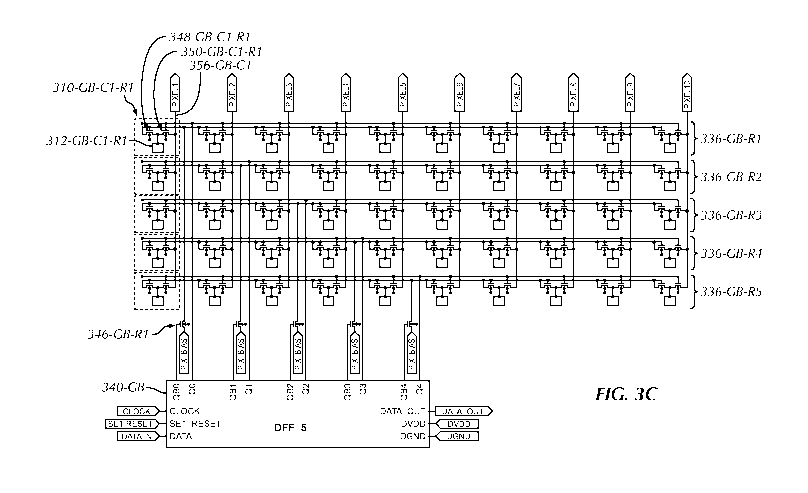
[0039] FIG. 3C illustrates an embodiment of a variable selection group with
50 sub-pixels arranged into 10 pixel groups and 5 selection subgroups.
[0040] FIG. 4A illustrates an exemplary active image area selection
configuration of an image sensor face according to embodiments of the
invention.
[0041] FIG. 4B illustrates some variations in active image area selection
configurations using six variable selection groups according to embodiments of
the
invention.
[0042] FIG. 5 illustrates an exemplary image capture device including a
sensor (imager) according to embodiments of the invention.
[0043] FIG. 6 illustrates a hardware block diagram of an exemplary image
processor that can be used with a sensor (imager) according to embodiments of
the
invention.
-8-
CA 02790853 2012-08-22
WO 2011/106568 PCT/US2011/026133
DETAILED DESCRIPTION
[0044] In the following description of preferred embodiments, reference is
made to the accompanying drawings which form a part hereof, and in which it is
shown by way of illustration specific embodiments in which the invention can
be
practiced. It is to be understood that other embodiments can be used and
structural
changes can be made without departing from the scope of the embodiments of
this
invention.
[0045] Variable Active Image Area Imager and Related Components
[0046] FIG. 3A illustrates an exemplary variable active image area image
sensor and related components according to embodiments of the invention. A
variable active image area image sensor according to embodiments of the
invention
may be used in various devices and applications, such as camera phones,
digital still
cameras, video, biometrics, security, surveillance, machine vision, medical
imaging,
barcode, touch screens, spectroscopy, optical character recognition, laser
triangulation, and position measurement
[0047] A variable active image area imager may comprise an image sensor
with a linear shape and multiple rows of LDEs, as shown by variable active
image
area image sensor 303 in FIG. 3A. As an example, variable active image area
imager 303 may comprise 2-20 rows and around 1000 columns of LDEs, or "sub-
pixels." Other embodiments may include an image sensor with a different shape,
such as a square, rectangle, circle, or oval.
[0048] The sub-pixels may be divided into one or more groups 320-G1, 320-
G2,. . ., 320-GN for variable selection. Variable selection group 320-G1
represents
an exemplary Group 1. Each variable selection group may comprise one or more
pixel groups. A pixel group may be arranged as a row, a column, a diagonal, or
any
other arbitrary arrangement of sub-pixels, according to application needs. For
instance, column 330-G1-C1 represents an exemplary pixel group in a column
arrangement at position Group 1-Column 1.
-9-
CA 02790853 2012-08-22
WO 2011/106568 PCT/US2011/026133
[0049] Sub-pixel 310-G1-C1-R1 represents an exemplary sub-pixel
(comprising a photodetector, e.g., a photodiode, a photogate) at position
Group 1-
Column 1-Row 1. Sub-pixel 310-G1-C1-R1 may be sensitive to light in various
ranges of the electromagnetic spectrum. One example is the infrared region,
e.g.,
700-900 nm. Other examples include one or more specific color regions, e.g.,
one or
more of red, yellow, green, blue, and violet. Another example is the
ultraviolet
region, e.g., 100-400 nm. Sub-pixels may also be monochrome. Still other
examples may include wavelength ranges beyond those mentioned here. In other
words, embodiments of the invention may be independent of any particular
wavelength range for sub-pixels.
[0050] Additionally, embodiments of the invention may be independent of
specific types of sub-pixels and image sensor architecture. For example, an
exemplary sub-pixel may belong to the Active Pixel Sensor type, as exemplified
in
U.S. Patent No. 5,949,483 to Fossum et al. For another example, an exemplary
sub-
pixel may belong to the Active Column Sensor type, as exemplified in U.S.
Patent
No. 6,084,229 to Pace et al.
[0051] For each variable selection group, there may be a corresponding
selector, as exemplified by selector 340-G1 for Group 1. (Selector 340-G2
would
correspond to group 320-G2, and selector 340-GN would correspond to group 320-
GN.) Selector 340-G1 may select a combination of one or more selection
subgroups
of sub-pixels in group 320-G1 through output 345-G1. A selection subgroup may
be
arranged as a row, a column, a diagonal, or any other arbitrary arrangement.
For
instance, the first row of sub-pixels in group 320-G1 (e.g., including sub-
pixels 310-
G1-C1-R1 and 310-G1-C2-R1) may be characterized as an exemplary selection
subgroup in a row arrangement at position Group 1-Row 1.
[0052] Furthermore, selector 340-G1 can be configured to select any
combination of one or more selection subgroups of sub-pixels in group 320-G1
through output 345-G1. For example, in the case of three selection subgroups
arranged as Rows 1, 2, and 3, selector 340-G1 can be configured to select any
combination of one or more of these three selection subgroups: {Row 11, {Row 2
{Row 3}, {Row 1, Row 2}, {Row 1, Row 3}, {Row 2, Row 3}, {Row 1, Row 2,
Row 3 } .
-10-
CA 02790853 2012-08-22
WO 2011/106568 PCT/US2011/026133
[0053] Every column in group 320-G1 may have the same selected one or
more rows. In column 330-G1-C1, a sub-pixel in a selected row may produce
output for column 330-G1-C1. If there is more than one selected row, sub-
pixels of
the selected rows would be selected to produce output for column 330-G1-C1.
Output for column 330-G1-C1 may be incorporated into an input 335-G1-C1 into a
readout 370. Values 375 corresponding to image capture data may be output from
readout 370 for processing, e.g., image processing. Readout 370 may comprise a
memory element, such as a shift register. Alternatively, readout 370 may
comprise
random access logic or a combination of shift register logic and random access
logic.
[0054] Variable Selection Group
[0055] FIG. 3B illustrates details of an exemplary variable selection group
(e.g., 320-G1) of an exemplary variable active image area image sensor
according to
embodiments of the invention. For clarity, other component details of group
320-G1
have not been included in FIG. 3B.
[0056] Group 320-G1 may comprise one or more sets of circuitry associated
with corresponding pixel groups of sub-pixels. Each pixel group of variable
selection group 320-G1 may have a corresponding pixel group circuit. For
example,
pixel group circuit 333-G1-Cl represents circuitry associated with the
exemplary
pixel group arranged in a column at position Group 1-Column 1. For each
additional pixel group, group 320-G1 may comprise another pixel group circuit,
such as 333-G1-C2 for Group 1-Column 2.
[0057] In addition to variable row selection group 320-G1, groups 320-G2 to
320-GN may be similar, or even identical, to group 320-G1 with corresponding
reference characters with G2 to GN for Groups 2 to N. Each group 320-G1 to 320-
GN may have the same number of columns per group or each group 320-GI to 320-
GN may have different numbers of columns. Each group 320-G1 to 320-GN may
have the same number of rows per group or each group 320-G1 to 320-GN may
have different numbers of rows.
[0058] In group 320-G1, each column may comprise M rows of sub-pixel
photodetectors. For Group 1-Column 1, there are sub-pixel photodetectors 312-
G1-
-11-
CA 02790853 2012-08-22
WO 2011/106568 PCT/US2011/026133
Cl-R1 to 312-G1-C1-RM. For each sub-pixel photodetector, there may be a
selection gate. A selection gate may be any suitable gating element (e.g., a
field-
effect transistor (FET), a transmission gate). Selector 340-G1 may send a
control
signal345-G1-Rl to selection gate 350-G1-Cl-Rl for selecting a sub-pixel of a
selection subgroup. For instance, sub-pixel 310-G1-C1-R1 in FIG. 3A represents
a
sub-pixel of an exemplary selection subgroup at position Group 1-Row 1.
Selector
340-GI may send a control signal 345-G1-RM to selection gate 350-G1-Cl-RM for
selecting Row M. Each column may have the same number of rows, or different
columns may have different numbers of rows.
[0059] Incident light that carries a desired image may be converted into
image capture data values through the following exemplary process. Light
incident
onto sub-pixel 312-G1-Cl-R1 may be converted into an electrical signal, which
may
be output to selection gate 350-G1-C1-R1. Control signal345-G1-Rl may control
selection gate 350-G1-Cl-Rl to place a corresponding electrical signal onto a
common sense node 356-G1-C1. The electrical signal may be processed through
the
cooperation of reset switch 380-G1-C1, reset line signal 382-G1-C1, reset bias
384-
G1-C1, sense circuitry 390-G1-Cl, and capture circuitry 360-G1-Cl.
[0060] Sense circuitry 390-G1-C1 may generate an output representative of
the total electrical signal on the sense node 356-G1-C1. Sense circuitry 390-
G1-Cl
may be embodied in multiple variations. An exemplary embodiment may comprise
a sense FET connected to sense node 356-G1-C1, the sense FET also connected to
an amplifier that outputs an analog value for analog binning. Another
exemplary
embodiment may comprise an op-amp connected to sense node 356-G1-C1, the op-
amp configured into an applicable op-amp configuration (e.g., comparator,
integrator, gain amplifier) that outputs a digital value for digital binning.
[0061] The output of sense circuitry 390-G1-C1 can then be captured by
capture circuitry 360-G1-C1. In the case that sense circuitry 390-G1-C1
outputs an
analog value, capture circuitry 360-G1-C1 can include an analog-to-digital
converter
(ADC) that digitizes the output of sense circuitry 390-G1-C1. In the analog
case, an
analog value can be switched onto bus(es) for further processing or readout.
In the
digital case, a value representative of the total electrical signal can then
be
determined and stored in a memory element (e.g., a latch, an accumulator).
This
-12-
CA 02790853 2012-08-22
WO 2011/106568 PCT/US2011/026133
value can be read out for processing, e.g., image processing. In one
embodiment,
capture circuitry 360-G1-C1 may provide input 335-G1-C1 into readout 370 of
FIG.
3A. In another embodiment, capture circuitry 360-G1-C1 may be part of readout
370.
[0062] Data from pixel group circuit 333-G1-C1 may be understood as
"pixel" data. In the case that only one row is selected, common sense node 356-
G1-
C1 may have a total electrical signal corresponding to one sub-pixel. In this
case,
one sub-pixel may be understood as the size of the "pixel" data.
[0063] In the case that multiple rows are selected at the same time (e.g.,
three rows), common sense node 356-G1-C1 may have a total electrical signal
corresponding to multiple sub-pixels (e.g., three sub-pixels). Binning may be
understood as reading out more than one sub-pixel at a time. If multiple sub-
pixels
(e.g., three) are selected, the number of sub-pixels may be understood as the
size of
the "pixel" data from pixel group circuit 333-G1-C1. If multiple non-adjacent
sub-
pixels are selected (e.g., a set of 1 sub-pixel non-adjacent to another set of
2 adjacent
sub-pixels), "pixel" data from pixel group circuit 333-G1-C1 may be understood
as
incorporating image information from non-adjacent portions of the
corresponding
column. Additional teachings concerning binning may be found in U.S. Patent
No.
7,057,150 B2 to Zarnowski et al.
[0064] When a set of sub-pixels is selected in a column (i.e., one or more
sub-pixels), this set may be understood as a "pixel" of the column. The size
of this
pixel would be based on the number of sub-pixels in the set. The location of
this
pixel would be based on the location of selected row(s) in the column.
Additionally,
even if the set consists of two non-adjacent sub-pixels, one may still
consider such a
set as a pixel.
[0065] In addition to pixel group circuit 333-GI-CI, group 320-GI may
comprise additional sets of pixel group circuits, exemplified by pixel group
circuit
333-G1-C2. Pixel group circuit 333-G1-C2 may be similar, or even identical, to
pixel group circuit 333-G1-C1 with corresponding reference characters with C2
for
Column 2.
-13-
CA 02790853 2012-08-22
WO 2011/106568 PCT/US2011/026133
[0066] Within the same variable selection group (e.g., 350-G1), all the pixel
group circuits (e.g., 333-G1-C1, 333-G1-C2, etc.) may receive the same control
signals (e.g., 345-G1-R1 to 345-G1-RM) from the same selector (e.g., 340-G1).
Therefore, a selection subgroup (e.g., row selection) could be the same for
all the
pixel groups (e.g., columns) in the same variable selection group. In an
example
embodiment of group 320-G1 with 5 rows and 10 columns, if selector 340-G1
selects Rows 2-4, group 320-GI may have an active image area of a block of 30
sub-
pixels (3 rows of sub-pixels x 10 columns of sub-pixels = 30 sub-pixels).
[0067] In embodiments with a plurality of variable selection groups, the sub-
pixel selection for one variable selection group may be independent of the sub-
pixel
selection for another variable selection group. For example, the control
signals
provided by selector 340-G1 may be independent of the control signals provided
by
selector 340-G2.
[0068] In the previous disclosure of U.S. Patent Application No. 12/712,146
filed February 24, 2010, sub-pixels have been described as LDEs that can be
binned
together to form a larger pixel prior to readout. The process of binning the
sub-
pixels may effectively control the size of the pixel to be readout. If the
desired pixel
size is larger than a single sub-pixel, then binning can be utilized. The
selection of
binned sub-pixels in a pixel group may also control the location of a pixel.
Only the
sub-pixels aligned in position to the desired image may need to be readout.
[0069] During the design phase, a pixel group may be constructed to have
multiple sub-pixels. The minimum sub-pixel size may be set to fit the
application
need or set smaller to allow for finer positioning of selected sub-pixels. If
sub-pixel
binning is not desired for the application, then a value of only a single sub-
pixel may
be read out from a pixel group. Calibration may be performed to fine tune the
selection of sub-pixels according to which sub-pixels may be most closely
aligned to
the desired image. Such calibration may be performed during assembly or at any
time after assembly.
[0070] FIG. 3C illustrates an embodiment of a variable selection group with
50 sub-pixels arranged into 10 pixel groups and 5 selection subgroups. The
variable
selection group forms a block of sub-pixels. The pixel groups are arranged
into 10
columns of sub-pixels. The selection sub-groups are arranged into 5 rows of
sub-
-14-
CA 02790853 2012-08-22
WO 2011/106568 PCT/US2011/026133
pixels. The physical size of the group can be of any size according to
application
preferences.
[0071] Sub-pixel 310-GB-Cl-R1 represents an exemplary sub-pixel in the
group block at position Column 1-Row 1. Sub-pixel 310-GB-Cl-R1 may comprise
a FET as selection gate 350-GB-Cl-R1.
[0072] If selected by DFF output QO from selector 340-GB, selection gate
350-GB-Cl-R1 connects photodiode 312-GB-Cl-R1 to sense node 356-GB-C1. In
this embodiment, a sub-pixel may be selected if the DFF output QO to the gate
of
FET 350-GB-Cl-R1 is "high" or a digital "1," thus photodiode 312-GB-Cl-R1
would be connected to sense node 356-GB-C1. Sense node 356-GB-Cl can be
connected to sense circuitry (e.g., a buffering amplifier as a source
follower, an input
FET of an operational amplifier).
[0073] It can be seen that an enabled output of DFF-QO would select all the
sub-pixels of row 336-GB-R1 throughout their respective columns. In the same
manner, an enabled output of DFF-Q1 would select all the sub-pixels of row 336-
GB-R2 throughout their respective columns. Therefore, a combination of one or
more rows of sub-pixels can be selected based on DFF output Q0-Q4.
Furthermore,
any combination of one or more rows can be selected based on DFF output Q0-Q4.
Image capture information from each selected sub-pixel would transfer to the
sense
node of the corresponding column of the sub-pixel.
[0074] The selector 340-GB DFF block can be a shift register, as shown in
FIG. 3C. Selector 340-GB comprises 5 serially connected D flip-flops. Other
configurations are possible where the information indicating the selected sub-
pixels
can be held and stored until such information is reset or reprogrammed.
[0075] The following description provides timing information for operating
the embodiment of FIG. 3C. 5 clock cycles can be used to program the 5 serial
flip-
flops. To select row 336-GB-RS, DATA_IN may be "1" for DFF clock cycle 1 and
followed by "0" for DFF clock cycles 2-5. DFF outputs Q0-Q4 would be 00001,
selecting only row 336-GB-RS. Afterwards, the values on the all the column
sense
nodes would be read out, and these values would correspond to the values of
selected row 336-GB-RS. For other examples, DFF outputs Q0-Q4 as 01100 could
-15-
CA 02790853 2012-08-22
WO 2011/106568 PCT/US2011/026133
select rows 336-GB-R2, R3; and DFF outputs Q0-Q4 as 10110 could select rows
336-GB-R1, R3, R4.
[0076] Referring back to FIG. 3C, DFF outputs QB can also provide a useful
feature, such as minimizing crosstalk between neighboring sub-pixels related
to
blooming. As a photodiode converts incident light photons into electrical
charge,
the photodiode may saturate. Once the photodiode has been saturated, charge
may
spill over to neighboring photodiodes. This spillover may be known as
blooming.
[0077] The QB output of the flip-flops can be used to hold the non-selected
sub-pixels in a reset condition. For example, a FET can be used as row bias
gate
346-GB-R1 to connect a bias to the sub-pixels of row 336-GB-R1. In the case
that
row 336-GB-R1 is not selected for readout, Q1 may be "low" or "0," and QB 1
may
be "high" or "1." The gate of FET 346-GB-R1 would be "high" or "1" and be on.
The PIX_BIAS value would be put on sub-pixel bias gate 348-GB-Cl-R1.
Specifically, the PIX_BIAS value would be put on the gate and drain of FET 348-
GB-Cl-R1, connecting the PIX_BIAS onto photodiode 312-GB-Cl-R1.
[0078] Even if sub-pixel 310-GB-Cl-R1 is not selected for readout, its
photodiode 312-GB-Cl-R1 may still convert incident light photons into
electrical
charge. PIX_BIAS could hold the value of photodiode 312-GB-Cl-R1 to a
particular reference value to prevent the photodiode from collecting photon-
generated charge. The charge that is generated on non-selected sub-pixel 310-
GB-
C1-R1 could be drained off through PIX_BIAS. Thus, charge would not fill
photodiode 312-GB-Cl-R1 and would not spill over into neighboring sub-pixels,
thereby preventing or minimizing blooming. Otherwise, blooming may lead to a
nearby selected photodiode picking up unwanted charge from non-selected
photodiode 312-GB-Cl-R1. Such unwanted charge could adversely affect the image
capture information provided by the selected photodiode, thus reducing image
quality. Accordingly, low or no blooming may lead to better image quality.
[0079] Active Image Area Selection Configurations
[0080] Based on the teachings above, the sub-pixels of an image sensor can
be selected so that the active image area of the image sensor can be
configured into a
wide variety of arrangements. For each variable selection group, a selector
may
-16-
CA 02790853 2012-08-22
WO 2011/106568 PCT/US2011/026133
send control signals to select sub-pixels in the group that would form part of
the
active image area. In between image captures, a selector may alter its
selection of
sub-pixels so that a different active image area selection configuration can
be used
for each image capture.
[0081] In some embodiments, sub-pixels may be selected according to
addressing techniques. For example, a sub-pixel may have its own unique
address.
With addressing techniques, a selector can receive address information and
then
send control signals to selection gates based on the received address
information.
[0082] In some embodiments, sub-pixels may be selected according to
position information. For example, a selector for a variable selection group
(e.g.,
selector 340-G2 for group 320-G2) can simply receive row selection information
(e.g., selection of Rows 2-5), and then send control signals to select sub-
pixels based
on the row selection information (e.g., all the sub-pixels in Rows 2-5 for all
columns
in group 320-G2).
[0083] A selector may be simple and comprise just a memory element, such
as a shift register comprising flip-flops. As an example, a simple string of
values
held by flip-flops of the shift register may indicate the row selection for
all the
columns in a variable selection group. In some embodiments, the number of flip-
flops in a selector may equal the number of rows (i.e., the number of elements
in a
pixel group) in the corresponding variable selection group.
[0084] The shift registers could be programmed using a Data_In input, a
clock, and an optional reset. Flip-flops are small and could easily fit within
a narrow
space (e.g., within 20 microns) along the edge of an image sensor face. Such a
narrow space may barely increase the die size.
[0085] A selector may comprise other components (e.g., a processor,
additional logic) that can receive address or position information of selected
sub-
pixels in various forms and then process this information to produce suitable
control
signals to select the corresponding sub-pixels.
[0086] A selector may receive sub-pixel selection information from another
controlling component or the selector may be part of a larger controlling
component
that produces sub-pixel selection information.
-17-
CA 02790853 2012-08-22
WO 2011/106568 PCT/US2011/026133
[0087] An exemplary active image area selection configuration may be
linear. A linear configuration may be useful for capturing a linear image. For
capturing a linear image, the selected sub-pixels may be mainly along one
linear
axis. However, it would not be required for these sub-pixels to be aligned
along a
horizontal axis, i.e., a particular row of sub-pixels. That is, instead of
employing
conventional measures of physically aligning a linear image and the physical
dimensions of the image sensor face to have a particular alignment (e.g., a
specific
parallel alignment), the active image area of an image sensor can be
configured to
closely match the linear image.
[0088] FIG. 4A illustrates an exemplary active image area selection
configuration (e.g., 401) of an image sensor face (e.g., 402) according to
embodiments of the invention. FIG. 4A is intended to show principles related
to
embodiments of the invention and may not be drawn to exact scale. Face 402 may
have 10 rows and 1000 columns of sub-pixels. Each sub-pixel may have
dimensions
of 10 x 10 microns so that face 402 may have boundary dimensions of 100
microns
x 10 mm. Configuration 401 may be useful for capturing a linear image that has
an
alignment with respect to image sensor face 402 that is not parallel (e.g.,
diagonal).
[0089] A desired linear image may start at the sub-pixel located at position
Row 1-Column 1 at the top left of face 402 and continue down to an the maximum
angle to the sub-pixel located at position Row 10-Column 1000 at the bottom
right
of face 402. Configuration 401 with an active image area 403 may capture such
a
desired linear image. As this desired linear image may shift only one row
every 100
columns, configuration 401 may employ only 10 variable selection groups (1000
total columns / 100 columns per shift = 10 variable selection groups for
shifting).
For each variable selection group, a selector may control the location, size,
and
shape of the portion of the active image area (e.g., 404) in the variable
selection
group.
[0090] If face 402 is divided into 10 variable selection groups, it may be
sufficient to have only 10 sets of row selection information (one set for each
variable
selection group) instead of 1000 sets of row selection information (one set
for each
column). In other words, it may sufficient to have distinct row selection
information
for every 100 columns. Therefore, the requirements for row selection
information
-18-
CA 02790853 2012-08-22
WO 2011/106568 PCT/US2011/026133
may be greatly simplified. For example, only 10 distinct addresses may be
sufficient
to provide an active image area selection configuration that is aligned to the
entire
desired linear image.
[0091] If face 402 is divided into more than 10 variable selection groups
(e.g., 20 variable selection groups of 50 columns each), greater alignment
flexibility
may be provided. For example, a desired linear image may not span across all
1000
columns when the image is aligned at a steep angle across face 402. In this
case, it
may be unnecessary to use image information from all the variable selection
groups,
and finer resolution may provide closer alignment between the steeply angled
image
and the selected sub-pixels.
[0092] In some embodiments where a selector comprises flip-flops, consider
an example of 20 variable selection groups, each group having 10 rows and 50
columns of sub-pixels. For each variable selection group, a selector may
comprise
10 flip-flops (i.e., one flip-flop per row). In total, the corresponding
selectors would
employ 200 flip-flops (i.e., 10 flip-flops x 20 variable selection groups).
[0093] A useful technique is calibrating an image sensor. One type of
calibration may include calibrating the selection of sub-pixels so that one
image
sensor can have a variety of active image area selection configurations. One
method
for calibrating the selection of sub-pixels may comprise illuminating the
image
sensor face with a desired image (e.g., a linear bar of light), reading out
image
information from all the sub-pixels, extracting the captured image data, and
programming the image sensor selectors to select the sub-pixels that are
aligned
most closely with the position of the desired image.
[0094] Another type of calibration may include calibrating for background
conditions of an image capture field (e.g., ambient light, infrared light,
sunlight).
One method for doing so may comprise periodically taking background condition
measurements, determining differences between the background condition
measurements and image capture data, and processing image capture data to
compensate for the background conditions.
-19-
CA 02790853 2012-08-22
WO 2011/106568 PCT/US2011/026133
[0095] Instead of mechanical types of calibration, these electronic types of
calibration may be performed independent of the mechanical aspects of an image
sensor. For example, the physical position of an image sensor does not have to
be
altered or tested. Instead, the image sensor may be calibrated by different
electronic
programming. Additionally, mechanical types of calibration may be used in
combination with these electronic types of calibration.
[0096] Also, these electronic types of calibration may be performed
repeatedly and in various combinations to accommodate various conditions. For
instance, calibration may be performed in between image captures; with and
without
an input image to capture; during non-usage and usage; with and without
background light; and with different desired image locations, shapes, and
sizes.
[0097] Additionally, another useful technique is determining when re-
calibration is needed. For example, when image capture data indicates an
unexpected image capture, re-calibration may be needed. For instance, when an
input light is on and no light is indicated in the image capture data, re-
calibration
may be needed. In such a situation, image information from all the sub-pixels
may
be re-read as part of the re-calibration.
[0098] FIG. 4B illustrates some variations in active image area selection
configurations using six variable selection groups according to embodiments of
the
invention. Configuration 412 shows a straight line of one row of sub-pixels.
[0099] One variation is varying the height of a selection subgroup of sub-
pixels. Configuration 414 shows a tall, straight line of three adjacent,
binned rows
of sub-pixels. Configuration 416 shows line segments with varying heights in
each
variable selection group, according to the following arrangement of heights in
terms
of sub-pixels: 1, 3, 7, 5, 1, 3.
[00100] Another variation is varying position of a selection subgroup of sub-
pixels. Configuration 418 shows a straight line of one row of sub-pixels,
vertically
shifted up with respect to the line of configuration 416. Configuration 420
shows
line segments of two adjacent, binned rows of sub-pixels. The line segments
have
varying vertical positions, arranged like an angled line. Configuration 422
shows
line segments of three adjacent, binned rows of sub-pixels. The line segments
have
-20-
CA 02790853 2012-08-22
WO 2011/106568 PCT/US2011/026133
varying vertical positions, arranged like a curve. Configuration 424 shows
line
segments of three adjacent, binned rows of sub-pixels. The line segments have
varying vertical positions, arranged so that the active image area is non-
continuous.
[00101] Another variation is blanking variable selection groups.
Configuration 426 shows lines segments similar to configuration 424, but there
are
blank regions in the first, fourth, and sixth variable selection groups. In a
blank
variable selection group, no sub-pixels are selected.
[00102] Another variation is selecting non-adjacent sub-pixels. Configuration
428 shows lines segments similar to configuration 420, but with an additional
straight line similar to configuration 418.
[00103] Another variation is varying size of a variable selection group.
Configuration 430 shows six variable selection groups, each with a different
size.
[00104] Any of these variations may be combined with each other.
Configuration 432 shows an example of combined variations. The first, third,
and
fifth variable selection groups show selected sub-pixels. For varying heights,
each
group has selection subgroups with different heights of sub-pixels: the first
group
may have a segment of two adjacent, binned rows of sub-pixels; the third group
may
have a segment of four adjacent, binned rows of sub-pixels; and the fifth
group may
have a segment of one row of sub-pixels. For varying positions, each group has
selection subgroups with a different position. For blanking variable selection
groups, the second, fourth, and sixth groups are blank. For selecting non-
adjacent
sub-pixels, the first group has three non-adjacent segments of sub-pixels and
the
fifth group has four non-adjacent segments of sub-pixels. For varying size of
a
variable selection group, each of the six variable selection groups has a
different
size.
[00105] Readout of Image Capture Information
[00106] In the embodiment of FIGs. 3A and 3B, image capture information
from the face of variable active image area imager 303 can be provided per
column
(i.e., pixel group). That is, as image capture information is read out from
the
columns, image capture information from the face is collected.
-21-
CA 02790853 2012-08-22
WO 2011/106568 PCT/US2011/026133
[00107] In a column, the column's sub-pixels may produce output that
contains the image capture information of the column. For instance, column 330-
G1-C1 may provide input 335-G1-C1 into readout 370. The other columns of
variable active image area imager 303 may similarly provide corresponding
input
into readout 370. Readout 370 may include one or more memory elements for
storing the image capture information from variable active image area imager
303.
[00108] Regardless of the number of selected rows in a column, the image
capture information output by the entire column may be stored as one value.
For
example, in the case that only one row is selected (e.g., Row M), image
capture
information from just one sub-pixel (e.g., 310-G1-C1-RM) in a column (e.g.,
Column 1) may be stored as one value in capture circuitry (e.g., 370-G1-C1).
As
another example, in the case that two rows are selected, image capture
information
from two sub-pixels in the column may also be stored as one value in the
capture
circuitry. The values from multiple columns may be sampled all together at a
time
or sampled sequentially.
[00109] Therefore, the total number of values to process may correspond to a
number of columns of the variable active image area imager 303, instead of the
total
number of sub-pixels in those columns. Accordingly, the image capture
information
from the face of variable active image area imager 303 can be processed as one
row
of values, not multiple rows. For instance, if readout 370 includes a shift
register as
a memory element for storing the image capture information of the columns,
such a
shift register can shift out this image capture information of the columns as
one row
of values, not multiple rows. In contrast, the readout process for a typical
area array
imager may involve reading out multiple rows of values, one row at a time, to
collect all the image capture information from the face of the area array
imager.
Thus, variable active image area imager 303 may process much less information
than a typical area array imager, resulting in lower power consumption and
lower
requirements for processing power.
[00110] Additionally, in some embodiments, it may be unnecessary to process
image capture information from every column (i.e., pixel group) (or even from
every
variable selection group). Such embodiments may be practiced with selective
readout, such as reading out image capture information from some columns (or
from
-22-
CA 02790853 2012-08-22
WO 2011/106568 PCT/US2011/026133
some variable selection groups) without reading out image capture information
from
particular columns (or even from particular variable selection groups). Such
embodiments may also be practiced by reading out image capture information
from
every column (or from every variable selection group), discarding image
capture
information from particular columns (or from particular variable selection
groups),
and processing the remaining image capture information.
[00111] Image Capture Device
[00112] FIG. 5 illustrates an exemplary image capture device 500 including a
sensor 506 (imager) according to embodiments of the invention. Light 501 can
approach sensor 506 via one or more optional optical elements 502 (e.g.,
reflecting
element, deflecting element, refracting element, propagation medium). An
optional
shutter 504 can control the exposure of sensor 506 to light 501.
[00113] A controller 506 can contain a computer-readable storage medium, a
processor, and other logic for controlling operations of a sensor 508. As an
example, controller 506 can provide control signals for performing the sub-
pixel
selection operations described above, such as the selecting of sub-pixels by
selectors
340-G1, 340-G2,. .., 340-GN in FIG. 3A. Sensor 508 can operate in accordance
with the variable active image area image sensor teachings above. The computer-
readable storage medium may be embodied in various non-transitory forms, such
as
physical storage media (e.g., a hard disk, an EPROM, a CD-ROM, magnetic tape,
optical disks, RAM, flash memory).
[00114] In contrast to a computer-readable storage medium, the instructions
for controlling operations of sensor 508 may be carried in transitory forms.
An
exemplary transitory form could be a transitory propagating medium, such as
signals
per se).
[00115] Readout logic 510 can be coupled to sensor 508 for reading out
image capture information and for storing this information within an image
processor 512. Image processor 512 can contain memory, a processor, and other
logic for performing operations for processing the data of an image captured
by
sensor 508. The sensor (imager) along with the readout logic and image
processor
can be formed on a single imager chip.
-23-
CA 02790853 2012-08-22
WO 2011/106568 PCT/US2011/026133
[00116] Controller 506 may control operations of readout 510. Controller
506 may also control operations of image processor 512. Controller 506 can
comprise a field-programmable gate array (FPGA) or a microcontroller.
[00117] FIG. 6 illustrates a hardware block diagram of an exemplary image
processor 612 that can be used with a sensor (imager) according to embodiments
of
the invention. In FIG. 6, one or more processors 638 can be coupled to read-
only
memory 640, non-volatile read/write memory 642, and random-access memory 644,
which can store boot code, BIOS, firmware, software, and any tables necessary
to
perform the processing described above. Optionally, one or more hardware
interfaces 646 can be connected to the processor 638 and memory devices to
communicate with external devices such as PCs, storage devices, and the like.
Furthermore, one or more dedicated hardware blocks, engines, or state machines
648
can also be connected to the processor 638 and memory devices to perform
specific
processing operations.
[00118] Comparative Advantages
[00119] Embodiments of the variable active imager area image sensor may
provide notable advantages over conventional image sensors. By way of example,
in applications for capturing a linear aspect of an image, embodiments of the
variable active imager area image sensor may be used instead of a conventional
linear imager. Embodiments of the variable active image area imager can
provide
variable location, size, and shape of active image area, which can lead to
greater
flexibility in alignment and calibration considerations for the position,
size, and
shape of the image. Furthermore, embodiments of the variable active image area
imager can provide electronic types of calibration that can repeatedly adjust
to
different alignment conditions, independent of mechanical methods of
calibration
and alignment.
[00120] In the same applications for capturing a linear aspect of an image,
embodiments of the variable active imager area image sensor may be used
instead of
a conventional area array imager, as well. Embodiments of the variable active
image area imager and a conventional linear imager may provide similar, or
even the
same, amounts of image information to process. Specifically, a conventional
area
array imager and embodiments of the variable active image area imager may
-24-
CA 02790853 2012-08-22
WO 2011/106568 PCT/US2011/026133
similarly have two-dimensional faces. For a conventional area array imager,
image
information from the face may be read out from each of all the rows, one row
of
information at a time. Each row of information is based on information from
the
same row of LDEs. Each row may be chosen for readout, in a fixed or random
sequence. In contrast, for embodiments of the variable active image area
imager,
image information from the face may be read out from all selected rows as just
one
row of information. Also, sub-pixel selection in the variable active image
area
imager may be independent of any fixed or random sequence of choosing rows
that
eventually progresses through many different rows for a readout process. For
instance, sub-pixel selection may be based on application needs (e.g.,
calibration and
alignment issues). Accordingly, scanning of the face can be reduced and
focused on
regions of interest instead of the entire face. The one row of information may
be
based on information from a variety of LDE row selection configurations, and
some
of these configurations can include information from multiple rows of LDEs or
from
different rows of LDEs. Thus, similar to a conventional linear imager, using a
variable active image area imager may involve less processing power and lower
power consumption than a conventional area array imager.
[00121] Additionally, embodiments of the variable active image area imager
can select a subset of sub-pixels or a subset of image capture information
produced
by sub-pixels. Thus, the use of unnecessary sub-pixels or the use of
unnecessary
image capture information can be avoided, which can lead to less processing
and
lower power consumption and less image capture information with noise.
[00122] Furthermore, embodiments of the variable active image area imager
can keep sub-pixels that are not selected for readout in a reset condition.
This reset
condition can minimize crosstalk between neighboring sub-pixels related to
blooming, thus contributing to higher image quality.
[00123] Although embodiments of this invention have been fully described
with reference to the accompanying drawings, it is to be noted that various
changes
and modifications will become apparent to those skilled in the art. Such
changes
and modifications are to be understood as being included within the scope of
embodiments of this invention as defined by the appended claims.
-25-