Note: Descriptions are shown in the official language in which they were submitted.
CA 02791037 2012-08-23
LED MODULE AND METHOD OF MANUFACTURING THE SAME
FIELD OF THE INVENTION
[0001] The present disclosure relates to an LED module and a
method of manufacturing the same.
BACKGROUND OF THE INVENTION
[0002] Conventionally, in a general method of manufacturing
an LED module, a separate LED element manufactured by
assembling an LED element in a lead frame-shaped package and
coating the LED element by a fluorescent material is
installed on a surface of a PCB substrate to manufacture a
module for illumination.
[0003] However, as for the LED element manufactured in
accordance with this method, a heating property of the LED
element is deteriorated and a luminous efficiency becomes
decreased, and it is limited to obtain brightness of a
conventional light bulb with restriction on a size, and also,
cost of the LED element cannot be reduced.
[0004] In order to overcome such problems, there has been
suggested a chip on board (COB) method in which a metal core
PCB (MCPCB) substrate is used without a package and a LED is
directly assembled in the MCPCB substrate.
[0005] The MCPCB has a high thermal conductivity but a
material thereof is expensive. For mass production of the
MCPCB, investment in facilities such as a specially designed
- 1 -
CA 02791037 2012-08-23
facility for mass production needs to be followed. Further,
in manufacturing the MCPCB, it is difficult to perform a
micro process with a size of about 50um or less. Therefore,
it has been deemed that the COB method has a low efficiency
in manufacturing a LED module for illumination and the MCPCB
is costly and inappropriate for a module for illumination.
[0006] Although there has been a research on a high-
efficiency LED single chip capable of improving luminosity
of an element, such a chip is expensive and a size thereof
cannot be reduced since a specially designed package is
needed to improve a heat emitting property thereof and also,
cost of assembly is very high.
[0007] Accordingly, a more efficient manufacturing method of
an LED module is demanded.
[0008] Some embodiments of the present disclosure provide an
LED module and a method of manufacturing the LED module
capable of improving a luminous efficiency of an LED element
by improving a heat emitting property thereof when a high-
luminance LED module is manufactured and capable of
manufacturing a small-sized high-luminance LED module at low
cost by forming a low-luminance LED into a module.
[0009] Further, some embodiments of the present disclosure
provide an LED module and a method of manufacturing the LED
module capable of improving a light emitting property of
each LED element by installing a reflecting plate in each
element and capable of manufacturing modules in various
- 2 -
CA 02791037 2012-08-23
shapes, which makes it possible to manufacture a high-
luminance LED for illumination having various functions.
[0010] Furthermore, some embodiments of the present
disclosure provide an LED module and a method of
manufacturing the LED module capable of considerably
reducing a defect rate of a module and production cost per
unit by using a semiconductor process that makes it easy to
mass produce.
BRIEF SUMMARY OF THE INVENTION
In accordance with a first embodiment of the present
invention, there is provided a manufacturing method of an
LED module including: forming an insulating film on a
substrate; forming a first ground pad and a second ground
pad separated from each other on the insulating film;
forming a first division film that fills a space between the
first and second ground pads, a second division film
deposited on a surface of the first ground pad, and a third
division film deposited on a surface of the second ground
pad; forming a first partition layer of a predetermined
height on each of the division films; sputtering seed metal
to the substrate on which the first partition layer is
formed; forming a second partition layer of a
predetermined height on the first partition layer; forming a
first mirror connected with the first ground pad and a
second mirror connected with the second ground pad by
- 3 -
CA 02791037 2012-08-23
performing a metal plating process to the substrate on which
the second partition layer is formed; removing the first
and second partition layers; connecting a zener diode to the
first mirror and connecting an LED to the second mirror; and
depositing a fluorescent material so as to fill a space
formed by the first mirror and the second mirror.
In accordance with a second embodiment of the present
invention, there is provided a manufacturing method of an
LED module including: inserting a zener diode into a
substrate; forming an insulating film on the substrate;
forming a first ground pad and a second ground pad separated
from each other on the insulating film; forming a first
division film that fills a space between the first and
second ground pads, a second division film deposited on a
surface of the first ground pad, and a third division film
deposited on a surface of the second ground pad; forming a
first partition layer of a predetermined height on each of
the division films; sputtering seed metal to the substrate
on which the first partition layer is formed; forming a
second partition layer of a predetermined height on the
first partition layer; forming a first mirror connected with
the first ground pad and a second mirror connected with the
second ground pad by performing a metal plating process to
the substrate on which the second partition layer is formed;
removing the first and second partition layers; connecting
an LED to the second mirror; and depositing a fluorescent
- 4 -
CA 02791037 2012-08-23
material so as to fill a space formed by the first mirror
and the second mirror.
In accordance with a third embodiment of the present
invention, there is provided an LED module including: a
first ground pad and a second ground pad separated from each
other on a substrate on which an insulating film is formed;
a first mirror connected with a surface of the first ground
pad; a second mirror connected with a surface of the second
ground pad; a zener diode connected with the first mirror;
an LED positioned on a partial surface of the second mirror;
and a fluorescent material formed on the zener diode and the
LED, wherein the other surface of the first mirror and the
other surface of the second mirror face each other.
[0011] In view of the foregoing, it is possible to improve a
heat emitting property when a high-luminance LED module is
manufactured and possible to manufacture a small-sized high-
luminance LED module at low cost by forming a low-luminance
LED into a module.
[0012] Further, in view of the foregoing, it is possible to
improve a light emitting property of each LED element by
installing a reflecting plate in each element and possible
to manufacture modules in various shapes, which makes it
possible to manufacture a high-luminance LED for
illumination having various functions.
[0013] Furthermore, in view of the foregoing, it is possible
to considerably reduce a defect rate of a module and
- 5 -
CA 02791037 2012-08-23
production cost per unit by using a semiconductor process
which makes it easy to mass produce.
BRIEF DESCRIPTION OF THE DRAWINGS
[0014] Non-limiting and non-exhaustive embodiments will be
described in conjunction with the accompanying drawings.
Understanding that these drawings depict only several
embodiments in accordance with the disclosure and are,
therefore, not to be intended to limit its scope, the
disclosure will be described with specificity and detail
through use of the accompanying drawings, in which:
[0015] Figs. la to lh are diagrams illustrating a
manufacturing method of an LED module in accordance with an
embodiment of the present disclosure;
Fig. 2 is a cross-sectional view of an LED module in
accordance with an embodiment of the present disclosure;
Figs. 3a to 3c are diagrams illustrating a
manufacturing method of an LED module in accordance with
another embodiment of the present disclosure; and
Fig. 4 is a flowchart of a manufacturing method of an
LED module in accordance with an embodiment of the present
disclosure.
DETAILED DESCRIPTION OF THE INVENTION
[0016] Hereinafter, embodiments of the present invention
will be described in detail with reference to the
- 6 -
CA 02791037 2012-08-23
accompanying drawings so that the present invention may be
readily implemented by those skilled in the art. However,
it is to be noted that the present invention is not limited
to the embodiments but can be realized in various other ways.
In the drawings, parts irrelevant to the description are
omitted for the simplicity of explanation, and like
reference numerals denote like parts through the whole
document.
[0017] Through the whole document, the term "connected to"
or "coupled to" that is used to designate a connection or
coupling of one element to another element includes both a
case that an element is "directly connected or coupled to"
another element and a case that an element is
"electronically connected or coupled to" another element via
still another element. Further, the term "comprises or
includes" and/or "comprising or including" used in the
document means that one or more other components, steps,
operation and/or existence or addition of elements are not
excluded in addition to the described components, steps,
operation and/or elements.
[0018] Figs. la to lh are diagrams illustrating a
manufacturing method of an LED module in accordance with an
embodiment of the present disclosure.
[0019] An LED module in accordance with an embodiment of the
present disclosure includes a first ground pad 142 and a
second ground pad 144 which are separately formed on a
- 7 -
CA 02791037 2012-08-23
substrate 110 on which an insulating film 120 is formed, a
first mirror 182 of which a surface is connected with the
first ground pad 142, a second mirror 184 of which a surface
is connected with the second ground pad 144, a zener diode
191 connected with the first mirror 182, an LED 192
positioned on a partial surface of the second mirror 184,
and a fluorescent material 194 formed on the zener diode 191
and the LED 192, and the other surface of the first mirror
182 and the other surface of the second mirror 184 may face
each other. Hereinafter, a manufacturing method of the LED
module will be explained in more detail.
[0020] Above all, as depicted in Fig. la, the insulating
film 120 is formed on the substrate 110. To be specific, Al
metal is deposited on the Si substrate 110 and an anodic
aluminum oxide (AAO) layer having nano pores of 5 nm or less
is formed by anodic oxidation and then, a silicon oxide
(SiO2) layer is deposited by using a plasma chemical vapor
deposition apparatus to manufacture the insulating film 120
for a LED module. Details of the process of manufacturing
the insulating film 120 may be found in prior art (Korean
Patent No. 10-0899894) of the present applicant.
[0021] Thereafter, as depicted in Fig. lb, a ground pad 140
is formed on the insulating film 120 and includes the first
ground pad 142 and the second ground pad 144 which are
separated from each other. Here, seed metal may be
sputtered to the insulating film 120 and a photo process and
- 8 -
9 CA 02791037 2012-08-23
a metal plating process using a photoresist layer 130 for
manufacturing the first ground pad 142 and the second ground
pad 144 may be performed, so that the first ground pad 142
and the second ground pad 144 may be formed.
[0022] To be more specific, Ti or Au as seed metal for
electroplating is sputtered and coated with a photosensitive
film and a pattern for manufacturing a ground pad is formed
by a photo process. Then, a ground pad is manufactured with
Cu or Au by electroplating.
[0023] Subsequently, as depicted in Fig. lc, a division film
150 is formed and includes a first division film 151
configured to fill a gap between the ground pads 142 and 144,
a second division film 152 configured to be layered on a
surface of the first ground pad 142, and a third division
film 153 configured to be layered on a surface of the second
ground pad 144.
[0024] Here, the first division film 151 to the third
division film 153 may be formed by coating the first ground
pad 142 and the second ground pad 144 with a polymer.
[0025] Then, as depicted in Fig. ld, a first partition layer
160 of a predetermined height is formed on the division film
150. Here, the first partition layer 160 may be formed by
layering a first photoresist layer on the substrate 110 on
which the division film 150 is formed and etching the first
photoresist layer such that a part of the first and second
ground pads 142 and 144 is exposed.
- 9 -
CA 02791037 2012-08-23
[0026] Thereafter, as depicted in Fig. le, seed metal 162 is
sputtered to the substrate 110 on which the first partition
layer 160 is formed.
[0027] Further, as depicted in Fig. if, a second partition
layer 170 of a predetermined height is formed on the first
partition layer 160. To be specific, a second photoresist
layer is layered on the substrate 110 to which a sputtering
process is performed and the second photoresist layer is
etched such that a part of the first and second ground pads
142 and 144 is exposed and an entire upper surface 164 of
the first partition layer 160 formed on the first division
film 151 is covered by the second photoresist layer.
[0028] Here, the second partition layer 170 may be formed
such that the entire upper surface 164 of the first
partition layer 160 formed on the first division film 151 is
covered by the second partition layer 170. Further, the
second partition layer 170 may be formed so as to expose a
part of upper surfaces 166 and 168 of the first partition
layers 160 formed on the second and third division films 152
and 153, respectively, by the second partition layer 170.
With this configuration, it is possible to prevent a mirror
180 from being formed around the first partition layer 160
formed on the first division film 151.
[0029] Subsequently, as depicted in Fig. lg, by performing a
metal plating process to the substrate 110 on which the
second partition layer 170 is formed, a first mirror 182
- 10 -
CA 02791037 2012-08-23
connected with the first ground pad 142 and a second mirror
184 connected with the second ground pad 144 are formed.
Here, the first mirror 182 and the second mirror 184 may be
formed by performing an electroplating process to the
substrate 110, on which the second partition layer 170 is
formed, with Ni, Su, Cu, Au and Ag.
[0030] Thus, as depicted in the drawing, a structure of the
mirror 180 may include the first partition layer 160, the
seed metal sputtered to the first partition layer 160, and
the second partition layer 170 that covers a part of the
sputtered seed metal.
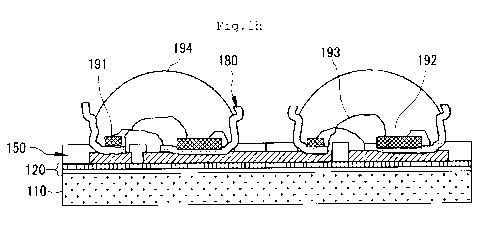
[0031] Then, as depicted in Fig. lh, the first partition
layer 160 and the second partition layer 170 are removed.
[0032] Thereafter, the zener diode 191 is connected with the
first mirror 182 and the LED 192 is connected with the
second mirror 184. Further, Au bonding wires 193 are
installed for electric wiring and the fluorescent material
194 is deposited so as to fill a space formed by the first
mirror 182 and the second mirror 184.
[0033] Fig. 2 is a cross-sectional view of an LED module
manufactured by the process depicted in Figs. la to lh in
accordance with an embodiment of the present disclosure.
[0034] As depicted in Fig. 2, with the LED module
manufactured by the above-described process, it is possible
to improve a light emitting property by installing a
reflecting plate in each LED element and possible to
- 11 -
CA 02791037 2012-08-23
manufacture modules in various shapes, which makes it
possible to manufacture a high-luminance LED for
illumination having various functions.
[0035] Further, it is possible to considerably reduce a
defect rate of a module and production cost per unit by
using a semiconductor process that makes it easy to mass
produce.
[0036] Furthermore, it is possible to assemble LEDs having
various color ranks in a single module, which makes it
possible to manufacture a sensitive lighting apparatus using
an LED.
[0037] Figs. 3a to 3c are diagrams illustrating a
manufacturing method of an LED module in accordance with
another embodiment of the present disclosure.
[0038] As depicted in Fig. 3a, before an insulating film 120
is formed on a substrate 110, a zener diode 191 may be
inserted into the substrate 110. Here, the inserted zener
diode 191 may be positioned under a first mirror 182. If
the zener diode 191 is inserted beforehand, a process may be
more simplified and a small-sized LED module can be
manufactured.
[0039] As depicted in Fig. 3b, a driver IC (Integrated
Circuit) 120 may be installed on the insulating film 120 of
the LED module. That is, the bare driver IC 200 of the LED
may be installed on the manufactured LED module and bonding
wires may be installed, so that integration density of the
- 12 -
CA 02791037 2012-08-23
module can be increased.
[0040] As depicted in Fig. 3c, an integrated passive device
210 may be integrated on the insulating film 120.
[0041] Thus, it is possible to improve a luminous efficiency
of the LED element by improving a heat emitting property
thereof when a high-luminance LED module is manufactured and
possible to manufacture a small-sized high-luminance LED
module at low cost by forming a low-luminance LED into a
module.
[0042] Fig. 4 is a flowchart of a manufacturing method of an
LED module in accordance with an embodiment of the present
disclosure.
[0043] First of all, an insulating film 120 is formed on a
substrate 110 (S101). Here, an aluminum oxide layer may be
formed on the substrate 110 and a silicon oxide (Si02) layer
may be deposited on the aluminum oxide layer, so that the
insulating film 120 may be formed. Further, in another
embodiment, a zener diode 191 may be inserted prior to this
step 5101.
[0044] Then, a first ground pad 142 and a second ground pad
144 which are separated from each other are formed on the
insulating film 120 (Sill). Here, seed metal may be
sputtered seed metal may be sputtered to the insulating film
120 and a photo process and a metal plating process may be
performed to manufacture the first ground pad 142 and the
second ground pad 144. As the seed metal, Ti or Au may be
- 13 -
CA 02791037 2012-08-23
used and Cu or Au may be used in the metal plating process.
[0045] Subsequently, a first division film 151 configured to
fill a gap between the ground pads, a second division film
152 configured to be layered on a surface of the first
ground pad 142, and a third division film 153 configured to
be layered on a surface of the second ground pad 144 are
formed (S121) Here, the first division film 151 to the
third division film 153 may be formed by coating the first
ground pad 142 and the second ground pad 144 with a polymer.
[0046] Then, a first partition layer 160 of a predetermined
height is formed on each division film (S131). Here, the
first partition layer 160 may be formed by layering a first
photoresist layer on the substrate 110 on which the division
film is formed and etching the first photoresist layer such
that a part of the first and second ground pads 142 and 144
is exposed.
[0047] Thereafter, seed metal is sputtered to the substrate
110 on which the first partition layer 160 is formed (S141).
[0048] Further, a second partition layer 170 of a
predetermined height is formed on the first partition layer
160 (S151) . Here, the second partition layer 170 may be
formed such that an entire upper surface 164 of the first
partition layer 160 formed on the first division film 151 is
covered by the second partition layer 170. Further, the
second partition layer 170 may be formed so as to expose a
part of upper surfaces 166 and 168 of the first partition
- 14 -
CA 02791037 2012-08-23
layers 160 formed on the second and third division films 152
and 153, respectively, by the second partition layer 170.
[0049] Subsequently, by performing a metal plating process
to the substrate 110 on which the second partition layer 170
is formed, a first mirror 182 connected with the first
ground pad 142 and a second mirror 184 connected with the
second ground pad 144 are formed (S161) The first mirror
182 and the second mirror 184 may be formed by performing an
electroplating process to the substrate 110, on which the
second partition layer 170 is formed, with Ni, Su, Cu, Au
and Ag.
[0050] Then, the first partition layer 160 and the second
partition layer 170 are removed (S171).
[0051] Thereafter, the zener diode 191 is connected with the
first mirror 182 and an LED 192 is connected with the second
mirror 184 (S181).
[0052] Subsequently, a fluorescent material 194 is deposited
so as to fill a space formed by the first mirror 182 and the
second mirror 184 (S191).
[0053] Meanwhile, in another embodiment, a driver IC 200 and
an integrated passive device 210 may be integrated together
on an insulating film 120 of an LED module.
[0054] The above description of the present invention is
provided for the purpose of illustration, and it would be
understood by those skilled in the art that various changes
and modifications may be made without changing technical
- 15 -
CA 02791037 2012-08-23
conception and essential features of the present invention.
Thus, it is clear that the above-described embodiments are
illustrative in all aspects and do not limit the present
invention. For example, each component described to be of a
single type can be implemented in a distributed manner.
Likewise, components described to be distributed can be
implemented in a combined manner.
[0055] The scope of the present invention is defined by the
following claims rather than by the detailed description of
the embodiment. It shall be understood that all
modifications and embodiments conceived from the meaning and
scope of the claims and their equivalents are included in
the scope of the present invention.
- 16 -