Note: Descriptions are shown in the official language in which they were submitted.
CA 02791607 2012-10-03
DIGITAL TO ANALOG CONVERTER
TECHNICAL FIELD
[0001 The present disclosure relates to a digital to analog converter and, in
particular, to a digital to
analog converter having a corrective term for gradient error.
BACKGROUND
[0002] Digital to analog converters (DAC) are commonly used analog blocks,
which play an important
role of converting a value in the digital domain to a value in the analog
domain. Generally, DACs
can be characterized into two groups. The first group includes DACs that
operate at Nyquist rate
(hereinafter referred to as "Nyquist DACs"), which is twice the maximum input
signal frequency,
allowing the input signal to be recovered without distortion. The second group
of DACs include
DACs that operate at a sampling rate higher than the Nyquist rate (hereinafter
referred to as
"oversampled DACs"). Oversampled DACs can achieve higher resolution without
increasing
complexity; however, this increased resolution comes at decreased conversion
rate. This is
because a more precise value is generated through the process of averaging
over time. As an
example, 0.5LSB can be produced by putting out a 1 followed by a zero which
averages to 0.5
over two time steps. However, the added resolution in the example is achieved
by trading time
and the cost is that the DAC can only provide this extra resolution to input
signals with half the
Nyquist rate.
[0003] A common implementation of DAC uses an array of current sources, which
are selectively
turned on to create an analog output proportional to the magnitude of the
digital value. Some
exemplary implementations of such DACs include current-steering DACs, switched-
capacitor
DACs and resistor-string DACs. However, due to practical limitations (e.g.
manufacturing),
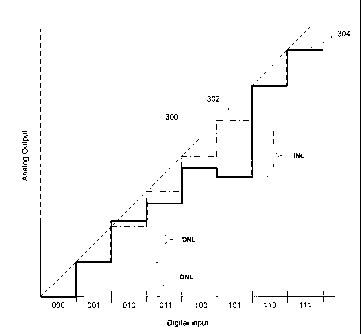
systematic errors are introduced into the conversion. One example of such
systematic errors is
gradient error created by inconsistencies in the silicon wafer, including
thermal, doping and
oxide thickness gradients. This can cause component properties to vary along a
particular
direction. Since DACs are built through arraying identical devices in two
dimensions, the output
produced by different components exhibit the same gradient in their
current/voltage output. The
result is that the output of the array of current sources is non-linear,
leading to Integral Non-
Linearity (INL) and Differential Non-Linearity (DNL).
1
08919330EP
CA 02791607 2012-10-03
[0004] There are known ways to cope with INL and DNL. One commonly used
technique is to
randomize the selection of the current sources to improve the INL and DNL.
Other techniques
include reordering the selection of the current sources in an effort to cancel
out the effects of
gradient errors, thus improving INL and DNL, and using a separate calibration
DAC that uses a
look-up table to produce a compensating current that cancels out the
systematic effects of INL
and DNL. However, these known techniques require an additional DAC which must
now
produce the exact compensation which is somehow characterized over a large
number of
DACs, averaged and represented as look-up table (LUT) entries. These entries
apply to all the
DACs over process and temperature corners and produce limited compensation
ability. The
compensating DAC and the associated LUT also take up space and current
consumption and
provide compensation ability to the extent of applicability of the calibration
values.
[0005] Another widely used approach provides the compensation by alternating
the selection of next
current cell elements such that the gradient is cancelled by inherent
selection of successive
devices. As input is increased the gradient is cancelled by choosing next
addressed element to
be on the opposite side of the gradient. However, this method requires the
knowledge of
gradient a priori in order to device a scheme of switching selection. This is
unfortunate if the
expected gradient turns out to be different than the actual gradient as the
scheme will no longer
provide the intended correction. Also, if the gradient changes from one lot to
another or from
one fabrication plant to another, there is no efficient way of determining a
compensation scheme
that would work across all the devices since the solution is hard-wired.
[0006] Accordingly, a DAC that addresses at least some of these disadvantages
is highly desirable.
BRIEF DESCRIPTION OF THE DRAWINGS
[0007] Further features and advantages of the present technology will become
apparent from the
following detailed description, taken in combination with the appended
drawings, in which:
FIG. 1 illustrates a block diagram for a hybrid DAC according to an embodiment
of the present
technology;
FIG. 2 illustrates an exemplary implementation of the hybrid DAC shown in FIG.
1;
FIG. 3 illustrates an exemplary digital to analog output showing the actual
output and the ideal
output;
2
08919330EP
CA 02791607 2012-10-03
FIG. 4 illustrates exemplary vertical and horizontal gradients in a current
source;
FIG. 5 illustrates a DAC according to another embodiment of the present
technology; and
FIG. 6 illustrates a DAC according to a further embodiment of the present
technology.
[00081 It will be noted that throughout the appended drawings, like features
are identified by like
reference numerals.
DETAILED DESCRIPTION
[0009] Embodiments are described below, by way of example only, with reference
to FIGS. 1-6.
[0010] In the present disclosure, a DAC that corrects systematic errors
arising from vertical gradient or
horizontal gradient or both is disclosed. The DAC includes a gradient
correction module that
generates a correction term based on the systematic error that is modelled
using, for example, a
second-order polynomial. The correction term is then applied to the signal
path in the digital
domain or applied to the output of the digital-to-analog converter in the
analog domain.
Furthermore, a digital-to-analog converter having a Nyquist DAC and an
oversampled DAC is
disclosed. When the oversampled DAC is enabled, the resolution of the Nyquist
DAC may be
increased while slowing the conversion rate.
[0011] In this specification and the appended claims, the singular forms "a,"
"an," and "the" include
plural references unless the context clearly dictates otherwise. Unless
defined otherwise, all
technical and scientific terms used herein have the same meaning as commonly
understood to
one of ordinary skill in the art to which this disclosure belongs.
[0012] It will be further understood that the terms "comprises" or
"comprising", or both when used in
this specification, specify the presence of stated features, integers, steps,
operations, elements,
and/or components, but do not preclude the presence or addition of one or more
other features,
integers, steps, operations, elements, components, and/or groups thereof.
[0013] In accordance with one embodiment of the present disclosure, there is
provided a digital-to-
analog converter (DAC). The DAC comprises a data input for receiving a digital
value; a current
source comprising an array of current source elements, the array of current
source elements for
producing an analog value; a current source selector for selectively
activating at least one of the
current source elements in the current source based on the digital value; a
gradient correction
3
08919330EP
CA 02791607 2012-10-03
module for generating a correction term based on a model of gradient error,
the correction term
being applied to the data input or being combined with the analog value
produced by the current
source; and a data output for outputting the analog value corresponding to the
digital value.
[0014] In some embodiments, the model of the gradient error is based on a
vertical gradient error.
[0015] In some embodiments, the vertical gradient error is modelled using a
second-order polynomial.
[0016] In some embodiments, the current source selector comprises a binary
coded part and a
thermometer coded part.
[0017] In some embodiments, the model of the gradient error is a second-order
polynomial based on a
vertical gradient error, the second-order polynomial expressed as
IOff = c2 (din - d .id )2 + c, (din - dm,d) , wherein diõ represents the
digital input into the
thermometer coded part, dmid represents the digital input corresponding to the
row in the
thermometer coded part of the array around which the vertical gradient error
is centered and loll
represents the deviation of the data output from an ideal output.
[0018] In some(((( embodiments, the ((din term is the value of dco,r as
defined by
dcorr+C2((din+dcorr)-dmid)2+c1((din+dcorr)-dmid)=0'
[0019] In some embodiments, the correction term is dcorr = -c2 (d,n -dmid )2 -
c, (din - dmid) .
[0020] In some embodiments, the current source comprises an array of switched
current cells,
switched-capacitor current source or resistor string current source, or a
combination thereof.
[0021] In some embodiments, the current source selector comprises a fully
binary coded circuit.
[0022] In some embodiments, the DAC further comprises a second current source
comprising at least
one current source element, the at least one current source element for
producing a time-
dithered output that averages to an analog value less than least-significant
bit (LSB) size of the
DAC; and a time-dithered selector for selectively activating the at least one
current source
element in the second current source to produce the time-dithered output when
enabled.
[0023] In some embodiments, the time-dithered selector generates a time-
dithered sequence using a
sigma-delta modulator, or a pulse-width modulator, or both.
4
08919330EP
CA 02791607 2012-10-03
[0024] In accordance with another embodiment of the present disclosure, there
is provided a method
for providing analog values comprising: receiving a digital data input;
converting the digital data
input to an analog output; applying a test codeword to the digital data input;
outputting the
analog value corresponding to the digital value; measuring the analog output
based on the
applied test codeword; and generating a correction term based on a model of
gradient error, the
correction term being applied to the digital data input or being combined with
the analog output.
[0025] In some embodiments, the generating a correction term comprises finding
a best-fit gradient
model polynomial for the measured analog output. .
[0026] In accordance with another embodiment of the present disclosure, there
is provided a digital-to-
1o analog converter (DAC). The DAC comprises a data input for receiving a
digital value; and a
Nyquist DAC having: a first current source comprising an array of current
source elements, the
array of current source elements for producing an analog value; and current
source selector for
selectively activating at least one of the current source elements in the
first current source
based on the digital value. The DAC further comprises an oversampled DAC
including: a
second current source comprising at least one current source element, the at
least one current
source element for producing a time-dithered output that averages to an analog
value less than
least-significant bit (LSB) size of the Nyquist DAC; and a time-dithered
selector for selectively
activating the at least one current source element in the second current
source to produce the
time-dithered output when the oversampled DAC is enabled. The DAC further
comprises a data
output for outputting an analog value corresponding to the digital value by
combining the analog
value from the Nyquist DAC and the analog value from the oversampled DAC when
enabled.
[0027] In some embodiments, the first current source and the second current
source are arranged into
an MxN array of current source elements, wherein M is the number of rows in
the array and N is
the number of columns in the array.
[0028] In some embodiments, the time-dithered selector generates a time-
dithered sequence using a
sigma-delta modulator, or a pulse-width modulator, or both.
[0029] In some embodiments, the first current source comprises an array of
switched current cells,
switched-capacitor current source or resistor string current source, or a
combination thereof.
[0030] In some embodiments, the second current source comprises an array of
switched current cells,
switched-capacitor current source or resistor string current source, or a
combination thereof.
5
08919330EP
CA 02791607 2012-10-03
[00311 In some embodiments, the DAC further comprises a second Nyquist DAC for
generating a DC
offset compensation, the DC offset compensation being used to compensate for a
DC offset
present in the Nyquist DAC.
[0032] The basic structure of a hybrid DAC 100, according to an embodiment of
the present
technology, is shown in FIG. 1. The hybrid DAC 100 includes a data input for
receiving the
digital value (Din) and an analog output for outputting the analog value
(A0,t). To convert the
digital value to the analog value, the hybrid DAC 100 includes a current
source selector 102 to
selectively activate the array of current source elements in the first current
source 104. The
current source selector 102 and the first current source 104, along with the
data input and
analog output, operate at the Nyquist rate and thus form a Nyquist DAC. The
principle upon
which current steering DAC operates is to steer the current from the positive
side to the
negative side so as to increment or decrement the selected value from the
total value. In
addition to the Nyquist DAC, the hybrid DAC 100 includes an oversampled DAC
that can be
activated to increase the resolution of the Nyquist DAC when necessary. The
oversampled DAC
includes a time-dithered selector 106 and a second current source 108, which
includes at least
one current source element for producing a time-dithered output based on the
selection by the
time-dithered selector 106. While the first and second current sources 104,
108 are shown as
separate elements, it will be understood that they may be formed within a
single current cell
array as shown in FIG. 2. That is, second current source 108 can be added to
the main array at
any row location, for example but not limited to, as an additional row
adjacent to the first current
source 104. Moreover, the relational terms first and second are used solely to
distinguish one
from another entity without necessarily requiring or implying order. The time-
dithered output
averages to a value that is less than the least-significant bit (LSB) of the
Nyquist DAC. For
example, the time-dithered output may be 10101010 to produce an average value
of 0.5 over
eight sampling cycles, when the LSB of the Nyquist DAC is 1. In this example,
the smallest
value 10000000 will produce 0.125 LSB output, hence increasing resolution to
beyond 1 LSB at
the cost of slower conversion time (i.e. the input must be held for eight
cycles). The time-
dithered output is combined with the output from the Nyquist DAC to produce
the converted
analog value. Thus, when enabled, the oversampled DAC increases the resolution
of the DAC
while increasing the conversion time. When the oversampled DAC is disabled,
conversion is
performed at the Nyquist rate. The time-dithered signal may be produced, for
example but not
limited to, using PWM signal or by a noise shaping sigma-delta modulator.
6
08919330EP
CA 02791607 2012-10-03
[0033] Turning to FIG. 2, an exemplary implementation of the hybrid DAC 100 is
shown. In this
implementation, the current source selector 102 is implemented as a segmented
selection
circuit comprising a binary coded section 202 and a thermometer coded section
204. The binary
coded section 202 receives the first X bits of Din as input and the
thermometer coded section
204 receives the remaining bits (Y-X) of Din as input. For example, where Din
is a 12-bit digital
value, the binary coded section 202 may receive the first 5 bits of Din while
the thermometer
coded section 204 may receive the remaining 7 bits. The decoded outputs of the
binary coded
section 202 and thermometer coded section 204 selectively turn on the current
source elements
in the first current source 104 to generate the corresponding analog current
value of the digital
input. In FIG. 2, the first and second current sources 104, 108 (hereinafter
collectively referred
to as current source 104, 108) are stacked to produce an MxN array of current
sources
elements. This allows the current source 104, 108 to have a symmetric layout.
[0034] The use of a segmented selection circuit as the current source selector
has many advantages,
including ease of matching requirements between differently weighted current
sources and
elimination of other switching problems. Each line in the binary coded section
202 may be
hardcoded to drive one or more current source elements in one row of the array
of current
elements in the current source 104. For example, if the binary coded section
202 receives the
first 5 bits of Din, bito may be connected to 1 current source element in
row,, bit, may be
connected to 2 current source elements in row2, bit2 may be connected to 4
current source
elements in row3, bit3 may be connected to 8 current source elements in row4
and bit4 may be
connected to 16 current source elements in rows. The remaining current source
elements may
be left as dummy current source elements. Again, this achieves symmetry in the
layout of the
current source elements and relaxes the matching requirements. In another
implementation, the
current source element may be weighted according to the binary value.
[0035] As for the thermometer coded section 204, it converts the (Y-X) input
bits into a 2(Y-X) -1 bits
output, with each bit driving a current source element in the first current
source 104. Referring to
a thermometer coded section receiving 7 bits, Table 1 below illustrates the
number of current
source elements in the first current source 104 that are turned on for each of
the corresponding
digital input.
Din Logic # of Current
Source Elements
7
08919330EP
CA 02791607 2012-10-03
Required
0000000 0 0
0000001 2 1
0000010 2' 2
0000011 21+20 3
0000100 22 4
0000101 2 2+20 5
1000000 26 64
1111111 26+25+24+23+22+21 +20 127
Table 1: Thermometer encoding
[0036) So, if each current source element in the current source produces an
ideal output of 1 mA, the
output can be proportionally changed depending on the digital input Din. This
DAC would then
have a resolution of 1 mA/LSB.
[0037] Hybrid DAC 100 further includes an oversampled DAC. In the
implementation shown in FIG. 2,
the time-dithered selector 106 is implemented using a sigma-delta modulator
106 driving the
second current source 108. In this exemplary implementation, the sigma-delta
modulator 106 is
a 1-bit modulator and thus, the output of the sigma-delta modulator 106 is
connected to one row
of the array of current source elements in the current source 104, 108. In
other words, the
second current source 108 is configured to be a 1xN current source elements,
stacked with the
first current source 104 to produce a MxN array of current source elements. It
will be understood
that, depending on the sigma-delta modulator 106 or any other time-dithered
output generator,
such as a pulse-width modulator, one or more rows of the current source 104,
108 may be
operated. In an alternative implementation, a multi-bit sigma-delta modulator
may also drive
8
08919330EP
CA 02791607 2012-10-03
multiple unit cells in one of the rows of current source 104, 108 as shown in
FIG. 2. When the
sigma-delta modulator 106 is enabled, it creates a time-dithered output that,
when averaged,
creates a value that is smaller than the LSB (i.e. sub-LSB). Thus, by
producing a sub-LSB
value, the hybrid DAC 100 is able to increase the resolution of the Nyquist
DAC. An example
will now be described.
[0038] Table 2 illustrates an exemplary output of the Nyquist DAC (i.e.
current source selector 102 and
first current source 104), which for each digital value generates a
corresponding analog value.
As discussed in the example in this disclosure, assuming that LSB of this
Nyquist DAC
translates to 1 mA. However, in order to increase the resolution and create an
output, for
example, of 0.5mA, the sigma-delta modulator 106 is activated to output 101010
over 6
sampling cycles. As illustrated in Table 3, the output from the combination of
the sigma-delta
modulator 106 and the Nyquist DAC produces an average value of 0.5mA. Also
note that the
conversion rate of the hybrid DAC would operate at 1/6 the conversation rate
of the Nyquist
DAC. In other words, conversion time is traded-off to increase the resolution
of the hybrid DAC
100. While the sigma-delta modulator 106 was shown with a 1-bit output, it
will be understood
that the sigma-delta modulator 106 may be a multi-bit output, which may
increase the
conversion rate.
Digital Value Analog Value
000 OmA
001 1 mA
010 2mA
011 3mA
Table 2: Sample DAC output without Sigma-Delta Modulator
Digital Value Sub-LSB Analog Value Average Value
000 1 OmA + l mA = 1 mA 3mA = O.SmA
6
9
08919330EP
CA 02791607 2012-10-03
000 0 OmA
000 1 OmA + 1 mA = 1 mA
000 0 OmA
000 1 OmA + 1 mA = l mA
000 0 OmA
Table 3: DAC output with Sigma-Delta Modulator
[00391 This hybrid DAC has many applications where a Nyquist DAC at a
predetermined resolution is
required but, in certain instances, a higher resolution than the predetermined
resolution is
required. For example, let us consider the design of a single DAC that can
operate at high rate
with low resolution and lower rate with higher resolution. In the high speed
mode, it could be
used as an I/Q (in-phase/quadrature) DAC in a transmitter to convert digital
I/Q input to analog
I/Q waveforms. The analog I/Q waveforms are then fed to analog filters,
upconversion mixer
and PA (power amplifier) driver to obtain the RF transmitter output. A copy of
the same DAC
can be used as an Automatic Frequency Control (AFC) DAC to control the
frequency of the
reference to the PLL (phase-locked loop) of the transmitter/receiver by
decoding frequency
bursts and determining that the reference frequency needs an adjustment. Such
adjustments
are not needed frequently, however, the DAC must exhibit much higher
resolution (13-bits e.g.
compared to 11-bits for TX DACs) in this application. The slower, more
accurate DAC can also
be used to compensate for TX or RX DC offsets, or for providing ramp to the
power amplifier.
The advantage of using this scheme is to partition a DAC into a Nyquist part
that operates at
high frequency and a time-dithered part that provides higher resolution at
lower speed of
operation. For DAC waveforms that are not needed simultaneously, a single DAC
can drive
multiple outputs e.g. in a Time Division Duplex communication standard.
[0040] In a further embodiment, hybrid DAC 100 in FIG. 1 may have more than
one Nyquist DACs or
more than one oversampled DACs or any combination thereof to be collocated
with
independent inputs. Referring to FIG. 2, the current sources of multiple DACs
may be placed
adjacent to each other in a single structure with multiple control inputs
driving them. In this
08919330EP
CA 02791607 2012-10-03
configuration, a hybrid DAC structure can be viewed as multiple independent
DACs. Referring
to FIG 2, the current source 104, 108 includes array of current source
elements which may be
controlled by the different DACs. For example, the first 1 to X rows may
belong to a first Nyquist
DAC, the next (X+1) to Y rows may belong to a second Nyquist DAC, and the
remaining (Y+1)
to M rows (X<Y<M) may belong to the sigma-delta DAC. In this implementation,
the collocation
of the current sources has the advantage of improving gradient and mismatch
related errors.
Moreover, one of the two Nyquist DAC may be used to apply a DC offset to
compensate for the
inherent DC offset at the output of the other Nyquist DAC, such that the load
shared by the two
DACs sees no DC offset. Fine DC offset can be cancelled by adding an
additional row of current
source element with an independent sigma-delta DAC input to add resolution to
the cancelling
DC offset (since offsets do not change quickly and oversampling can be used to
trade slow
response with higher resolution).
[0041] As discussed in the present disclosure, DACs are often implemented
using an array of current
source elements, which are selectively turned on to create an analog output
proportional to the
magnitude of the digital value. The array of current source elements may be
implemented in a
variety of ways including a switched current source (i.e. combination of
differential current
switch and cascade current source), a switched-capacitor array and/or a
resistor string array
based voltage DACs. However, due to practical limitations, systematic
mismatches occur
between at least some of the current source elements in the array. Thus, while
the ideal output
produces an analog value that is linearly proportional to the digital value,
the actual output may
be non-linear due to systematic errors (e.g. gradient error). These systematic
errors can be
measured in terms of Integral Non-Linearity (INL) and Differential Non-
Linearity (DNL), an
example which is shown in FIG. 3. DNL refers to the difference between two
analog outputs
corresponding to adjacent digital inputs and INL refers to the maximum
deviation of the actual
analog output when compared to the ideal analog output. In FIG. 3, the ideal
output is shown as
output 302, which follows the linearly proportional line 300 and monotonically
increases by the
LSB size. However, because of systematic errors, the actual output 304 may
deviate from the
ideal output 302.
[0042] Both active and passive solutions have been proposed to lower INL and
DNL. Passive solutions
may include measuring the gradient error after fabrication of the current
source, and selectively
hard-wiring the current source elements to lower INL and DNL. For example, a
current source
element that is producing an analog value greater than 1 LSB may be paired
with a current
source element that is producing an analog value less than 1 LSB. Active
solutions also
11
08919330EP
CA 02791607 2012-10-03
similarly reorder the order in which the current source elements in the
current source are turned
on and off to effectively lower INL and DNL. Other active solutions include
randomizing or
pseudo-randomizing the selection order to lower INL and DNL.
[0043] To better combat INL and DNL without randomization or reordering the
selection of the current
source elements, the present disclosure determines a correction term based on
a gradient
model, and applies the correction term in the digital domain (i.e. in the
signal path of Din) or in
the analog domain (i.e. at the analog output). To determine the correction
term, a model of the
gradient error is created, which simulates the difference between the ideal
output and actual
output of the current source caused by the gradient in the current source.
[0044] Gradient error is an error caused by inconsistencies in the silicon
wafer, such as thermal,
doping and oxide thickness anomalies created during the manufacturing process.
There may
also be mechanically induced inconsistencies, for example near the edges of
the silicon wafer
where a cut was made. Gradients can be characterized as being a vertical
gradient (i.e. gradient
error between cells in the y-direction) and a horizontal gradient (i.e.
gradient error between cells
in the x-direction). FIG. 4 shows a visual representation of vertical and
horizontal gradient. The
MxN array of current source elements in the current sources 400, 402 are shown
to have
vertical and horizontal gradients as indicated by the shaded areas. As shown,
vertical gradients
create differences between current source elements in the y-direction. The
current value
produced by a current source element in one row would be different from
another current source
element in another row that is affected by the gradient. If a ramp signal is
applied at the input to
cause selection of increasingly more rows and the difference of the actual
output to the ideal
output will be referred to as an error waveform, the error waveform will have
two components to
it: the first caused by systematic gradient and the second due to random
mismatches. As
disclosed in the present disclosure, the systematic gradient is modelled using
a polynomial. The
polynomial is then fit into the error waveform to determine the systematic
part of the error. In the
exemplary embodiment, a second order polynomial is fit to represent the
systematic gradient
and applied for correction.
[0045) By contrast, horizontal gradients create differences between current
source elements in the x-
direction. However, unlike vertical gradients, all current source elements in
the row are equally
affected and thus, the output of the thermometer coded part (e.g. 204 in FIG.
2) is not scaled by
the error quantity. That is because the horizontal gradient affects all rows
the same way in the
thermometer coded part. However, horizontal gradient will affect the binary
coded part (e.g. 202
12
08919330EP
CA 02791607 2012-10-03
in FIG. 2) which uses only a part of a row, as the rest of the current cells
in the row may be
dummy cells, and can be largely corrected by centering the binary cells around
the center of the
horizontal array. Alternatively, the horizontal gradient in the binary coded
part may be modelled
as with the vertical gradient, described below.
[0046] To correct for the vertical gradient in the thermometer coded part of
the array, a model is
created that takes into consideration the vertical gradient in the current
source array, which
typically consumes more than 99% of the DAC current source area. Generally,
the vertical
gradient in the current source can be expressed as a second order polynomial:
IQfr = c2 (d, - d,n;(j)2 + c1(din - dn,,d) , where d;, represents the digital
input into the thermometer
coded part of the DAC, did represents the digital input corresponding to the
row in the
thermometer coded part of the array around which the vertical gradient is
centered and /off
represents the deviation of the actual output from the ideal output. While
this model takes into
consideration the codeword inputted into the thermometer coded part of the DAC
(i.e. dn), it will
be understood that it can be expanded to the entire DAC (thermometer and
binary coded part)
depending on the implementation of the current source selector. For example,
where the current
source selector is implemented using a segmented selection circuit, d;,, may
be replaced with
the input to the entire DAC. The correcting polynomial for the binary part
will compute the
distance of the binary row from dmid and apply the polynomial correction.
[0047] The calculated /off can then be added to the input or output to remove
the difference between
the actual output and the ideal output. However, prior to the calculation, the
coefficients c, and
c2, and did must be determined through a calibration process. The calibration
process involves
inputting a series of test code-words into the data input, measuring the
output of the DAC based
on the series of test code-words, and finding a best-fit gradient model
polynomial for the
measured output. For example, the test code-words can be a ramp signal. This
calibration may
be done on a per-DAC basis or for a plurality of DACs. One advantage of this
approach is that
compensation for the gradient error can be determined after the construction
of the DAC,
eliminating any guess work or discrepancies between the expected gradient and
the actual
gradient. While the model is represented using a second-order polynomial, it
will be understood
that a higher order polynomial may be used to increase accuracy. It will
further be understood
that, while the described model considers the effects of the vertical
gradient, the model may well
be configured to consider the horizontal gradient. This can be achieved by
revising the model as
a two-dimensional model, which takes into consideration the offset of the
current source
13
08919330EP
CA 02791607 2012-10-03
elements in both the x and y direction. The compensation for the horizontal
gradient will then be
applied to the binary coded part as well as the time dithered bits.
[0048] Now turning to FIG. 5, a DAC 500 according to another embodiment of the
present technology
is disclosed. In DAC 500, there is included a current source selector 502, and
a current source
504, which may be similarly implemented as current source selector 102 and
first current source
104. For example, the current source selector 502 may be a fully binary coded
circuit,
segmented selection circuit or any other selection circuit suitable to work
with a current source.
As for the current source 504, it may be, for example, an array of switched
current cells,
switched-capacitor or resistor string array based voltage source. Furthermore,
it will be
understood that DAC 500 may also include a time-dithered selector (such as 106
in FIG. 1) and
a second current source (such as 108 in FIG. 1), which may be enabled to
increase the
resolution of the DAC 500 all being driven by the sum of the compensation
circuit 506 output
and the input (i.e. compensated output of the adder in DAC 500).
[0049] In addition, the DAC 500 includes a gradient correction module 506 in
the input signal d;,,, which
adds a correction term to the input signal d;,, in the digital domain based on
the vertical gradient
model. The output of the DAC 500, with the gradient correction module 506
disabled, can be
expressed as Ion, = din + Iõff , which can be expanded out to
Ion, = din + c2 (din - d,n1d )2 + c1(d,n - d,,,,,). Thus, in order to cancel
out the gradient error, a
correction term door is applied to the signal path (i.e. d;,, + d 01), and the
new output can be
expressed as Ion, _ (din + dCorr) + c2 ((din + d,.orr) - dn,,d )2 + c1((d,n +
d,orr) - dm,d). For the output
to equal the ideal output, drorr + c2 ((d,n + dcorr) - d,,,,,, )2 + c1((d,n +
dcorr) - d,n,d) = 0 , which can be
solved for dcorr to arrive at the compensation codeword to apply to the signal
path in the digital
domain. Each dcorr calculated for d;,, may be stored in memory and retrieved
for subsequent use.
In another preferred implementation, value for dcorr may be simplified to
increase the
performance of the DAC 500. In this implementation, door is simply equated to
-c2(d;n -d,,,,,)2 -c1(din -dn,;d).
[0050] Another implementation of the present technology is shown in FIG. 6
where the output of the
gradient correction module 606 is combined with the output of the Nyquist DAC.
The correction
term determined by the gradient correction module 606 is applied using the
correction current
source 604, which may comprise at least one current source element to generate
the correction
14
08919330EP
CA 02791607 2012-10-03
term. Since the correction term is applied in the analog domain, the
correction term may be
expressed as I(,ff = c2 (D,,1 - Dm d)2 + c, (D,,, - D,,,(,) . The compensating
DAC is collocated with
the main DAC and uses some of the rows of the current source 104, 108. In one
implementation, in order to generate a more accurate /off, the output of the
gradient correction
module 606 may use an oversampled clock to generate a time-dithered sequence
that averages
to the desired value of the correction term. The time-dithered sequence may be
generated, for
example, using a sigma-delta modulator, or a pulse-width modulator.
[0051] The correction term applied to embodiments shown in FIG. 5 and FIG. 6
may span over the
entire code-word including the binary and the oversampled DAC. The oversampled
DAC may
be operated with an independent clock at N x fs, where fs is the clock applied
to the Nyquist
DAC and N is the oversampling ratio. Hence, the correction term has a higher
resolution than
the LSB of the Nyquist DAC.
[0052] As with the DAC 500 in FIG. 5, the Nyquist DAC in FIG. 6 is comprised
of the current source
selector 602 and the current source 604, which may be similarly implemented as
current source
selector 102 and first current source 104. In one implementation, the current
source selector
602 may be a fully binary coded circuit. In another implementation, the
current source selector
602 may be a segmented selection circuit having a binary coded section and a
thermometer
coded section. As for the current source 604, it may be, for example, an array
of switched
current cells, switched-capacitor or resistor string array voltage source.
Furthermore, it will be
understood that DAC 600 may also include an oversampled DAC comprised of a
time-dithered
selector (such as 106 in FIG. 1) and a second current source (such as 108 in
FIG. 1), which
may be enabled to increase the resolution of the Nyquist DAC.
[0053] While the present technology has been described in terms of specific
implementations and
configurations, further modifications, variations, modifications and
refinements may be made
without departing from the inventive concepts presented herein. The scope of
the exclusive right
sought by the Applicant(s) is therefore intended to be limited solely by the
appended claims.
08919330EP