Note: Descriptions are shown in the official language in which they were submitted.
81731859
ELECTRONIC CONTROL UNIT
BACKGROUND OF THE INVENTION
The present invention relates to an electronic control unit.
Priority is claimed on Japanese Patent Application Nos. 2011-231806,
2011-231808, and 2011-231809, filed on October 21,2011.
Field of the Invention
In recent years, vehicles (hereinafter, collectively referred to as plug-in
vehicles)
such as electric cars or plug-in hybrid cars that can be charged by the use of
an external
power supply have been increasingly put to practical use. A dedicated charging
cable
having a control unit called a CCID (Charge Circuit Interrupt Device) is used
to connect
a plug-in vehicle to an external power supply.
The standard on an interface between the charging cable and the plug-in
vehicle
is defined by the "SAE (Electric Vehicle Conductive Charge Coupler) standard"
of the
U.S. or the "General Requirements for Electric Vehicle Conductive Charging
System (the
Japanese Electric Vehicle Standard)" of Japan. The charging sequence of a plug-
in
vehicle defined in the standard is substantially as follows.
First, a CCID of a charging cable transmits a control pilot signal
(hereinafter,
abbreviated as a pilot signal) to a charging-control ECU (Electronic Control
Unit)
mounted on a plug-in vehicle and determines that the charging cable is
connected to the
plug-in vehicle when the voltage of the pilot signal is changed from an
initial value VI
(for example, 12 V) to V2 (for example, 9 V).
Then, the CCID of the charging cable informs the ECU of the plug-in vehicle of
CA 2792310 2018-10-16
CA 02792310 2012-10-17
2
the rated current of a power supply facility by transmitting a pilot signal
with a duty ratio
corresponding to the rated current of the power supply facility (including an
external
power supply and a charging cable).
The ECU of the plug-in vehicle informs the CCID of the charging cable of the
completion of the preparation for charging by changing the voltage of the
pilot signal
from V2 to V3 (for example, 6 V).
Then, when detecting that the voltage of the pilot signal has changed from V2
to
V3, the CCID of the charging cable determines that the preparation of charging
of the
plug-in vehicle side is completed, and turns on a relay used to supply the
power of the
external power supply to the plug-in vehicle (that is, starts the supply of
power).
In this way, the pilot signal is a signal essential for controlling the
charging of
the plug-in vehicle and it is very important to detect abnormality of the
pilot signal. For
example, Japanese Unexamined Patent Application, First Publication No. 2009-
71989
discloses a technique of connecting a control line used for transmission of a
pilot signal
on a plug-in vehicle to the ground via a switch and detecting a disconnection
of a pilot
signal line extending from a charging port of the plug-in vehicle to an ECU
based on a
change in potential of the control line when the switch is turned on.
Description of Related Art
As described above, the ECU of the plug-in vehicle is provided with a pilot
voltage setting circuit used to change the voltage of a pilot signal
transmitted from the
CCID of the charging cable in a stepwise manner. In general, the pilot voltage
setting
circuit is a serial circuit of a pull-down resistor and a switching element,
which is
connected between the pilot signal line and the ground in the ECU.
When the processor in the ECU changes the voltage of a pilot signal, the
CA 02792310 2012-10-17
=
3
switching element of the pilot voltage setting circuit is turned on.
When the switching element of the pilot voltage setting circuit is out of
order,
the voltage of a pilot signal cannot be changed and thus a circuit for
diagnosing the
disorder of the switching element is necessary. However, such a circuit is not
disclosed
in Japanese Unexamined Patent Application, First Publication No. 2009-71989.
In the technique described in Japanese Unexamined Patent Application, First
Publication No. 2009-71989, a switching connecting the pilot signal line to
the ground is
provided and it is determined that the pilot signal line is normal (no
disconnection) when
the potential of the pilot signal line is dropped to the ground level by
turning on the
switch. However, when the pilot signal line is subjected to an earth fault,
the potential
of the pilot signal line also becomes the ground level. Accordingly, the pilot
signal line
may be erroneously determined to be normal, while actually being abnormal.
The invention is made in consideration of the above-mentioned circumstances
and an object thereof is to provide an electronic control unit that can
diagnose at least one
of an abnormality of a switching element disposed in a pilot voltage setting
circuit so as
to change a pilot signal in a stepwise manner and an abnormality of a pilot
signal line
including disconnection and earth fault.
SUMMARY OF THE INVENTION
The present invention employs the following configurations to solve the above
problems.
(1) According to an aspect of the invention, there is provided an
electronic control
unit that is mounted on a vehicle which is configured to be charged with an
external
power supply and that receives a pilot signal via a charging cable before
being supplied
with a power when the vehicle is connected to the external power supply via
the charging
CA 02792310 2012-10-17
4
cable, the electronic control unit including: a control line that is connected
to a pilot
signal line connecting a charging cable connector disposed in the vehicle to
the electronic
control unit; a processor that performs a process necessary for the control of
charging
based on the pilot signal input via the control line; a pilot voltage setting
circuit that is
connected between the control line and a ground and that includes a serial
circuit of a
pull-down resistor and a switching element controlled by the processor; a
voltage supply
circuit that includes at least one of a first diagnosis voltage supply circuit
supplying a
first diagnosis voltage to the control line under control of the processor and
a second
diagnosis voltage supply circuit supplying a second diagnosis voltage to the
pilot signal
line via an abnormality diagnosis line connected to the pilot signal line at
the charging
cable connector under the control of the processor; and an abnormality
diagnosis circuit
that is connected to the pull-down resistor and the switching element and that
outputs an
abnormality diagnosis result signal of at least one of the switching element
and the pilot
signal line to the processor, wherein the processor performs at least one of a
first
diagnosis process of determining whether or not the switching element is
abnormal based
on an output signal of the abnormality diagnosis circuit obtained when turning
on and off
the switching element while controlling the first diagnosis voltage supply
circuit to
supply the first diagnosis voltage to the control line and a second diagnosis
process of
determining whether or not the pilot signal line is abnormal based on the
output signal of
the abnormality diagnosis circuit obtained when controlling the second
diagnosis voltage
supply circuit to supply the second diagnosis voltage to the pilot signal line
in a state
where the switching element is maintained in OFF state.
(2) In the electronic control unit described in (1) above, the voltage
supply circuit
may include only the first diagnosis voltage supply circuit, and the processor
may
determine whether or not the switching element is abnormal based on a level of
the
CA 02792310 2012-10-17
output signal of the abnormality diagnosis circuit obtained when turning on
and off the
switching element while controlling the first diagnosis voltage supply circuit
to supply
the first diagnosis voltage of a fixed voltage to the control line as the
first diagnosis
process.
5 (3) In the electronic control unit described in (1) above, the
voltage supply circuit
may include only the first diagnosis voltage supply circuit, and the processor
may
determine whether or not the switching element is abnormal based on an edge of
the
output signal of the abnormality diagnosis circuit obtained when turning on
and off the
switching element while controlling the first diagnosis voltage supply circuit
to supply
the pulse-like first diagnosis voltage with a predetermined frequency to the
control line
as the first diagnosis process.
(4) In the electronic control unit described in (1) above, the voltage
supply circuit
may include only the second diagnosis voltage supply circuit, and the
processor may
determine whether or not the pilot signal line is abnormal based on a level of
the output
signal of the abnormality diagnosis circuit obtained when controlling the
second
diagnosis voltage supply circuit to supply the second diagnosis voltage of a
fixed voltage
to the pilot signal line in a state where the switching element is maintained
in OFF state
as the second diagnosis process.
(5) In the electronic control unit described in (1) above, the voltage
supply circuit
may include only the second diagnosis voltage supply circuit, and the
processor may
determine whether or not the pilot signal line is abnormal based on an edge of
the output
signal of the abnormality diagnosis circuit obtained when controlling the
second
diagnosis voltage supply circuit to supply the pulse-like second diagnosis
voltage with a
predetermined frequency to the pilot signal line in a state where the
switching element is
.. maintained in OFF state as the second diagnosis process.
CA 02792310 2012-10-17
6
(6) In the electronic control unit described in (4) or (5) above, the
processor may
perform the second diagnosis process when the charging cable is not connected
to the
vehicle.
(7) In the electronic control unit described in (1) above, the voltage
supply circuit
may include both the first diagnosis voltage supply circuit and the second
diagnosis
voltage supply circuit, and the processor may perform the second diagnosis
process after
performing the first diagnosis process.
(8) In the electronic control unit described in (7) above, the processor
may first
determine whether or not the switching element is abnormal based on a level of
the
output signal of the abnormality diagnosis circuit obtained when turning on
and off the
switching element while controlling the first diagnosis voltage supply circuit
to supply
the first diagnosis voltage of a fixed voltage to the control line as the
first diagnosis
process, and then may determine whether or not the pilot signal line is
abnormal based on
a level of the output signal of the abnormality diagnosis circuit obtained
when controlling
the second diagnosis voltage supply circuit to supply the second diagnosis
voltage of a
fixed voltage to the pilot signal line in a state where the switching element
is maintained
in OFF state as the second diagnosis process.
(9) In the electronic control unit described in (7) above, the processor
may first
determines whether or not the switching element is abnormal based on an edge
of the
output signal of the abnormality diagnosis circuit obtained when turning on
and off the
switching element while controlling the first diagnosis voltage supply circuit
to supply
the pulse-like first diagnosis voltage with a predetermined frequency to the
control line
as the first diagnosis process, and then may determine whether or not the
pilot signal line
is abnormal based on an edge of the output signal of the abnormality diagnosis
circuit
obtained when controlling the second diagnosis voltage supply circuit to
supply the
CA 02792310 2012-10-17
7
pulse-like second diagnosis voltage with a predetermined frequency to the
pilot signal
line in a state where the switching element is maintained in OFF state as the
second
diagnosis process.
(10) In the electronic control unit described in any one of (7) to (9)
above, the
processor may perform the second diagnosis process after performing the first
diagnosis
process when the charging cable is not connected to the vehicle.
BRIEF DESCRIPTION OF THE DRAWINGS
FIG. 1 is a schematic diagram illustrating the configuration of a vehicle
charging
system according to a first embodiment of the invention.
FIG 2 is a diagram illustrating the internal configuration of a charging-
control
ECU 33A according to the first embodiment.
FIG. 3 is a timing diagram illustrating a charging operation of the vehicle
charging system.
FIG. 4A is a timing diagram illustrating an operation (first example) of the
charging-control ECU 33A diagnosing abnormality of a first switching element I
04b.
FIG. 48 is a timing diagram illustrating an operation (second example) of the
charging-control ECU 33A diagnosing abnormality of the first switching element
104b.
FIG. 5 is a schematic diagram illustrating the configuration of a vehicle
charging
system according to a second embodiment of the invention.
FIG. 6 is a diagram illustrating the internal configuration of a charging-
control
ECU 33B according to the second embodiment.
FIG. 7A is a timing diagram illustrating an operation (first example) of the
charging-control ECU 33B diagnosing abnormality of a pilot signal line 34.
FIG. 7B is a timing diagram illustrating an operation (second example) of the
CA 02792310 2012-10-17
8
charging-control ECU 33B diagnosing abnormality of the pilot signal line 34.
FIG. 8 is a schematic diagram illustrating the configuration of a vehicle
charging
system according to a third embodiment of the invention.
FIG. 9 is a diagram illustrating the internal configuration of a charging-
control
ECU 33C according to the third embodiment of the invention.
FIG. 10A is a timing diagram illustrating an operation (first example) of the
charging-control ECU 33C diagnosing abnormality of a first switching element
104b and
a pilot signal line 34.
FIG. 10B is a timing diagram illustrating an operation (second example) of the
charging-control ECU 33C diagnosing abnormality of the first switching element
104b
and the pilot signal line 34.
DETAILED DESCRIPTION OF THE INVENTION
Hereinafter, an embodiment of the invention will be described in detail with
reference to the accompanying drawings.
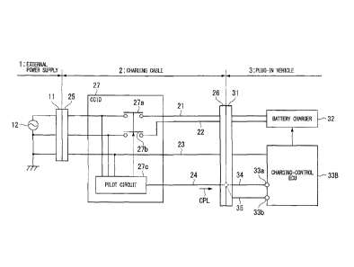
A first embodiment of the invention will be first described. FIG. 1 is a
schematic diagram illustrating the configuration of a vehicle charging system
according
to a first embodiment of the invention. As shown in FIG 1, the vehicle
charging system
according to the first embodiment includes an external power supply 1, a
charging cable
2, and a plug-in vehicle 3. The external power supply 1 includes a power
receptacle 11
with a ground terminal disposed, for example, in a house and an AC power
supply
(commercial power supply) 12 supplying single-phase AC power to the power
receptacle
11.
The charging cable 2 includes two power supply lines 21 and 22, a ground line
23, a pilot line 24, a plug 25, and a cable-side coupler 26, and a CCID 27. In
each of
CA 02792310 2012-10-17
9
the power supply lines 21 and 22 and the ground line 23, an end thereof is
connected to
the plug 25 and the other end thereof is connected to the cable-side coupler
26. An end
of the pilot line 24 is connected to the CCID 27 (specifically, a pilot
circuit 27c) and the
other end thereof is connected to the cable-side coupler 26.
By connecting the plug 25 to the power receptacle 11, one end of each of the
power supply lines 21 and 22 is connected to the AC power supply 12 and one
end of the
ground line 23 is connected to the ground of the external power supply 1. By
connecting the cable-side coupler 26 to a vehicle-side coupler 31 of the plug-
in vehicle 3,
the other end of each of the power supply lines 21 and 22 is connected to a
battery
charger 32 of the plug-in vehicle 3 and the other end of each of the ground
line 23 and
the pilot line 24 is connected to a charging-control ECU 33A of the plug-in
vehicle 3.
The CCID 27 is a control unit that is disposed in the middle of the power
supply
lines 21 and 22 and the ground line 23, and includes relays 27a and 27b
disposed in the
middle of the power supply lines 21 and 22 and a pilot circuit 27c
transmitting a pilot
signal CPL to the charging-control ECU 33A of the plug-in vehicle 3 via the
pilot line 24
and controlling ON and OFF states of the relays 27a and 27b. The pilot circuit
27c is
connected to the power supply lines 21 and 22 and the ground line 23 and is
supplied
with a source voltage from the power supply lines 21 and 22 and with a ground
voltage
from the ground line 23.
The plug-in vehicle 3 is a vehicle which can be charged with the external
power
supply 1, such as an electric car or a plug-in hybrid car, and includes a
vehicle-side
coupler 31, a battery charger 32, and a charging-control ECU 33A. By
connecting the
cable-side coupler 26 of the charging cable 2 to the vehicle-side coupler 31,
the power
supply lines 21 and 22 are connected to the battery charger 32, and the ground
line 23
and the pilot line 24 are connected to the charging-control ECU 33A.
CA 02792310 2012-10-17
=
The battery charger 32 is a charging circuit that converts single-phase AC
power
supplied from the external power supply 1 via the charging cable 2 (the power
supply
lines 21 and 22) into DC power under the control of the charging-control ECU
33A and
that charges a driving battery (not shown) mounted on the plug-in vehicle 3
with the DC
5 power. The charging-control ECU 33A is an electronic control unit that
receives a pilot
signal CPL via the charging cable 2 before being supplied with the power when
the
plug-in vehicle 3 is connected to the external power supply 1 via the charging
cable 2 and
that performs a process necessary for the charging control of the driving
battery based on
the pilot signal CPL.
10 The charging-control ECU 33A includes a pilot signal input terminal 33a
connected to a pilot signal line 34 extending from the vehicle-side coupler 31
(the
charging cable connector) disposed in the plug-in vehicle 3 and used for
communication
of a pilot signal CPL.
FIG. 2 is a diagram illustrating the internal configuration of the charging-
control
ECU 33A according to the first embodiment. As shown in FIG 2, the charging-
control
ECU 33A includes an avalanche diode 101, a first diode 102, a first pull-down
resistor
103, a pilot voltage setting circuit 104, an input buffer 105, a first
diagnosis voltage
supply circuit 106, an abnormality diagnosis circuit 107, and a CPU 108.
The avalanche diode 101 has one end connected to the pilot signal input
terminal 33a and the other end connected to the ground and serves to hold the
voltage of
the pilot signal CPL (the voltage between the pilot signal input terminal 33a
and the
ground) input via the pilot signal input terminal 33a to be V1 (for example,
12 V) or
lower.
The first diode 102 has an anode terminal connected to the pilot signal input
terminal 33a and a cathode terminal connected to one end of the first pull-
down resistor
CA 02792310 2012-10-17
11
103 and serves to pass only a positive signal of the pilot signal CPL. The
first
pull-down resistor 103 has one end connected to the cathode terminal of the
first diode
102 and the other end connected to the ground and serves to change the
positive voltage
of the pilot signal CPL (that is, the voltage between the cathode terminal of
the first diode
102 and the ground) from Vito V2 (for example, 9 V).
The pilot voltage setting circuit 104 is a circuit that changes the positive
voltage
of the pilot signal CPL in a stepwise manner (for example, changes the voltage
from V2
to V3 (for example, 6 V)) under the control of the CPU 108. The pilot voltage
setting
circuit 104 includes a second pull-down resistor 104a and a first switching
element 104b,
for example, which is an npn-type transistor.
In the pilot voltage setting circuit 104, one end of the second pull-down
resistor
104a is connected to the cathode terminal of the first diode 102 (is connected
to a control
line CL extending from the pilot signal input terminal 33a to the input buffer
105) and the
other end thereof is connected to the collector terminal of the first
switching element
104b.
Here, the control line CL is a line for transmitting a pilot signal CPL to the
CPU
108 in the charging-control ECU 33A and is connected to the pilot signal line
34
connecting the vehicle-side coupler 31 to the charging-control ECU 33A with
the pilot
signal input terminal 33a therebetween.
The collector terminal of the first switching element 104b is connected to the
other end of the first pull-down resistor 104a, the emitter terminal thereof
is connected to
the ground, and the base terminal thereof is connected to a first control
signal output port
CTl_OUT of the CPU 108. The first switching element 104b is switched between
ON
and OFF states based on a first control signal CT1 output from the first
control signal
output port CT I_OUT of the CPU 108 to the base terminal thereof.
CA 02792310 2012-10-17
=
12
In the pilot voltage setting circuit 104 having this configuration, when the
first
switching element 104b is in ON state, the other end of the second pull-down
resistor
104a is connected to the ground and the positive voltage of the pilot signal
CPL is
changed from V2 to V3.
The input buffer 105 is a buffer of which the input terminal is connected to
the
cathode terminal of the first diode 102 and the output terminal is connected
to a pilot
signal input port INT of the CPU 108. The pilot signal CPL is input to the
pilot signal
input port INT of the CPU 108 via the input buffer 105.
The first diagnosis voltage supply circuit 106 is a voltage supply circuit
that
supplies a first diagnosis voltage for diagnosing the abnormality of the first
switching
element 104b to the control line CL under the control of the CPU 108 and
includes a
second switching element 106a which is, for example, a pnp-type transistor, a
second
diode 106b, and two resistors 106c and 106d.
The emitter terminal of the second switching element 106a is connected to the
power supply line PL1, the collector terminal thereof is connected to the
control line CL
via the second diode 106b, and the base terminal thereof is connected to a
second control
signal output port CT2_OUT of the CPU 108 via the resistor 106c. The second
switching element 106a is switched between ON and OFF states based on a second
control signal CT2 output from the second control signal output port CT2_OUT
of the
CPU 108 to the base terminal thereof.
The charging-control ECU 33A includes a regulator that drops a main source
voltage V1GB supplied from a low-voltage battery mounted on the plug-in
vehicle 3
independently of a driving battery to generate a sub source voltage VREG. A
sub source
voltage VREG output from the regulator is applied to the power supply line PL
I .
The anode terminal of the second diode 106b is connected to the collector
CA 02792310 2012-10-17
13
terminal of the second switching element 106a and the cathode terminal thereof
is
connected to the control line CL. One end of the resistor 106c is connected to
the base
terminal of the second switching element 106a and the other end thereof is
connected to
the second control signal output port CT2OUT of the CPU 108. One end of the
resistor 106d is connected to the emitter terminal of the second switching
element 106a
and the other end thereof is connected to the other end of the resistor 106c.
In the first diagnosis voltage supply circuit 106 having this configuration,
when
the second switching element 106a is in ON state, the power supply line PL I
and the
control line CL are electrically connected to each other and the sub source
voltage VREG
is supplied as the first diagnosis voltage to the control line CL.
The abnormality diagnosis circuit 107 is a circuit that outputs a signal
indicating
that the comparison result of the voltage VcN of a connection point of the
second
pull-down resistor 104a and the first switching element 104b in the pilot
voltage setting
circuit 104 with the reference voltage VREF as the abnormality diagnosis
result of the first
switching element 104b and includes three resistors 107a, 107b, and 107c, a
capacitor
107d, and a comparator 107e.
One end of the resistor 107a is connected to the connection point of the
second
pull-down resistor 104a and the first switching element 104b in the pilot
voltage setting
circuit 104 and the other end thereof is connected to one end of the capacitor
107d and
the inverting input terminal of the comparator 107e. One end of the capacitor
107d is
connected to the other end of the resistor 107a and the inverting input
terminal of the
comparator 107e and the other end thereof is connected to the ground. The
resistor
107a and the capacitor 107d serve as a noise removing filter of the voltage
(the
connection point voltage VON) input to the inverting input terminal of the
comparator
107e.
CA 02792310 2012-10-17
=
=
14
One end of the resistor 107b is connected to a power supply line PL2 and the
other end thereof is connected to one end of the resistor 107c and the non-
inverting input
terminal of the comparator 107e, One end of the resistor 107c is connected to
the other
end of the resistor 107b and the non-inverting input terminal of the
comparator 107e and
the other end thereof is connected to the ground.
The charging-control ECU 33A includes a 5 V regulator that further drops the
sub source voltage VREG to generate a sub source voltage VAcc (for example, 5
V) in
addition to the above-mentioned regulator. The sub source voltage VACc output
from
the 5 V regulator is applied to the power supply line PL2. That is, when the
resistance
value of the resistor 107b is defined as R1 and the resistance value of the
resistor 107c is
defined as R2, the reference voltage VREF input to the non-inverting input
terminal of the
comparator 107e is expressed by R2.VAcc/(R1+R2).
The comparator 107e compares the connection point voltage VcN input to the
inverting input terminal with the reference voltage VREF input to the non-
inverting input
terminal and outputs a signal (diagnosis result signal) CR indicating the
comparison
result as the abnormality diagnosis result of the first switching element 104b
to a
diagnosis result signal input port CR_1N of the CPU 108. Specifically, the
comparator
107e outputs the diagnosis result signal CR of a high level when the
connection point
voltage VCN is lower than the reference voltage VREF, and outputs the
diagnosis result
signal CR of a low level when the connection point voltage VcN is higher than
or equal to
the reference voltage VREF.
The CPU 108 is a processor that performs a process necessary for the charging
control based on the pilot signal CPL input to the pilot signal input port TNT
via the input
buffer 105, and controls the pilot voltage setting circuit 104 (outputs the
first control
signal CT I ) to change the voltage of the pilot signal CPL in a stepwise
manner.
CA 02792310 2012-10-17
Although the details thereof will be described later, the CPU 108 has a
function
of determining whether or not the first switching element 104b is abnormal
based on the
output signal (that is, the diagnosis result signal CR) of the abnormality
diagnosis circuit
107 obtained when turning on and off the first switching element 104b while
controlling
5 the first diagnosis voltage supply circuit 106 (the second switching
element 106a) to
supply the first diagnosis voltage (that is, the sub source voltage VREG) to
the control line
CL as an abnormality diagnosis process (the first diagnosis process) of the
first switching
element 104b.
The operation of the vehicle charging system having the above-mentioned
10 configuration will be described below with reference to the timing
diagram of FIG. 3.
First, at time ti in FIG. 3, when the plug 25 of the charging cable 2 is
connected
to the power receptacle 11 of the external power supply I, the pilot circuit
27c of the
CCID 27 is supplied with power from the AC power supply 12 via the power
supply lines
21 and 22, is started up, and outputs the pilot signal CPL of a voltage value
Vi (12 V) via
15 the pilot line 24. At this time point, the relays 27a and 27b of the
CCID 27 are in OFF
state and the CPU 108 of the charging-control ECU 33A is in a sleep state.
As shown in FIG 3, when the CPU 108 is in the sleep state, the first control
signal CT1 output from the CPU 108 is at a low level. Accordingly, the first
switching
element 104b of the pilot voltage setting circuit 104 is in OFF state.
Subsequently, at time t2 in FIG 3, when the cable-side coupler 26 of the
charging cable 2 is connected to the vehicle-side coupler 31 of the plug-in
vehicle 3, the
pilot signal CPL is input to the pilot signal input terminal 33a of the
charging-control
ECU 33A, but the positive voltage of the pilot signal CPL (the voltage between
the
cathode terminal of the first diode 102 and the ground) is changed from Vito
V2 (9 V)
by the first pull-down resistor 103.
CA 02792310 2012-10-17
16
When the change in voltage of the pilot signal CPL (the change in voltage of
the
pilot line 24) is detected, the pilot circuit 27c of the CCID 27 determines
that the
charging cable 2 is connected to the plug-in vehicle 3 and informs the
charging-control
ECU 33A of the rated current of the power supply facility by transmitting the
pilot signal
CPL at a duty ratio corresponding to the rated current of the power supply
facility (the
external power supply 1 and the charging cable 2) at time t3 in FIG. 3.
When the CPU 108 of the charging-control ECU 33A starts up from the sleep
state at time t4 in a predetermined time after time t3, the CPU 108 measures
the duty
ratio of the pilot signal CPL input via the input buffer 105 to acquire the
rated current of
the power supply facility, then outputs the first control signal CT1 of a high
level at time
t5 in FIG 3 to switch the first switching element 104b to ON state, and
informs the CCID
27 of the charging cable 2 of the completion of the preparation for charging
by changing
the voltage of the pilot signal CPL from V2 to V3 (6 V).
When the pilot circuit 27c of the CCID 27 detects that the voltage of the
pilot
signal CPL (the voltage of the pilot line 24) is changed from V2 to V3, the
pilot circuit
27c determines that the preparation for charging of the plug-in vehicle 3 is
completed and
turns on the relays 27a and 27b for supplying the AC power of the external
power supply
1 to the plug-in vehicle 3 (that is, starts the supply of power). Accordingly,
the AC
power is supplied from the external power supply 1 to the battery charger 32
of the
plug-in vehicle 3 via the charging cable 2 (the power supply lines 21 and 22).
The CPU 108 of the charging-control ECU 33A appropriately controls the
charging of the driving battery by controlling the battery charger 32 based on
the rated
current of the power supply facility acquired from the duty ratio of the pilot
signal CPL.
In this way, since the stepwise change of the voltage of the pilot signal CPL
in
the charging-control ECU 33A means that the CCID 27 of the charging cable 2 is
CA 02792310 2012-10-17
17
informed of the state of the plug-in vehicle 3 side, this is very important in
the charging
control of the driving battery. When abnormality occurs in the first switching
element
104b of the pilot voltage setting circuit 104, the voltage of the pilot signal
CPL cannot be
changed from V2 to V3 and thus there is a problem in that the supply of power
to the
plug-in vehicle 3 via the charging cable 2 is not started.
Therefore, it is important to diagnose the abnormality of the first switching
element 104b. In the first embodiment, the CPU 108 of the charging-control ECU
33A
performs the abnormality diagnosis process (the first diagnosis process) of
the first
switching element 104b in accordance with the following sequence. Two examples
of
the first diagnosis will be described below, but any thereof may be employed.
The CPU
108 performs the following first diagnosis process when the charging cable 2
is not
connected to the plug-in vehicle 3 (for example, when the plug-in vehicle 3 is
traveling).
This is because the above-mentioned charging operation is interrupted when the
first
diagnosis process is performed in a state where the charging cable 2 is
connected to the
plug-in vehicle 3.
A first example of the first diagnosis process performed by the CPU 108 will
be
described below with reference to the timing diagram of FIG. 4A.
First, the CPU 108 controls the first switching element 104b and the second
switching element 106a into OFF state by setting the first control signal CT1
to a low
level and setting the second control signal CT2 to a high level as an initial
process. At
this time, since the connection point voltage VcN is lower than the reference
voltage VREF,
the diagnosis result signal CR of a high level is output from the comparator
107e.
Subsequently, after time ti 1 in FIG 4A, the CPU 108 holds the second
switching
element 106a in ON state by setting the second control signal CT2 to a low
level.
Accordingly, after time tll, the first diagnosis voltage of a fixed voltage
(the sub source
CA 02792310 2012-10-17
=
18
voltage VREG) is supplied from the first diagnosis voltage supply circuit 106
to the
control line CL.
Subsequently, as described above, the CPU 108 switches the first switching
element 104b to ON state by setting the first control signal CT1 to a high
level at time
t12 while controlling the first diagnosis voltage supply circuit 106 to supply
the first
diagnosis voltage of a fixed voltage to the control line CL, and then switches
the first
switching element 104b to OFF state again by setting the first control signal
CT1 to a low
level at time t13.
Accordingly, when the first switching element 104b is normal, the connection
point voltage VcN is higher than the reference voltage VREF in the period of
times tl 1 to
t12 and thus the diagnosis result signal CR of a low level is output from the
comparator
107e. In the period of times t12 to t13, the connection point voltage VcN is
lower than
the reference voltage VREF and thus the diagnosis result signal CR of a high
level is
output from the comparator 107e. After time t13, the connection point voltage
Vc=N is
higher than the reference voltage VREF and thus the diagnosis result signal CR
of a low
level is output from the comparator 107e.
As described above, the CPU 108 determines whether or not the first switching
element 104b is abnormal based on the level of the diagnosis result signal CR
obtained
when turning on and off the first switching element 104b while controlling the
first
diagnosis voltage supply circuit 106 to supply the first diagnosis voltage of
a fixed
voltage to the control line CL.
Specifically, the CPU 108 determines that the first switching element 104b is
normal when the diagnosis result signal CR is at the high level at the time of
turning on
the first switching element 104b and the diagnosis result signal CR is at the
low level at
the time of turning off the first switching element 104b in the state where
the second
CA 02792310 2012-10-17
19
switching element 106a is maintained in ON state.
The CPU 108 determines that the first switching element 104b is abnormal
(on-fixed malfunction) when the diagnosis result signal CR is at the high
level regardless
of ON and OFF states of the first switching element 104b in the state where
the second
switching element 106a is maintained in ON state, and determines that the
first switching
element 104b is abnormal (off-fixed malfunction) when the diagnosis result
signal CR is
at the low level regardless of ON and OFF states of the first switching
element 104b.
A second example of the first diagnosis process performed by the CPU 108 will
be described below with reference to the timing diagram of FIG. 4B.
First, similarly to the first example, the CPU 108 controls the first
switching
element 104b and the second switching element 106a into OFF state as an
initial process.
At this time, the diagnosis result signal CR of a high level is output from
the comparator
107e.
Subsequently, in the period of times t21 to t22 in FIG 4B, the CPU 108
controls
the second switching element 106a in a PWM manner by outputting the pulse-like
second control signal CT2 with a fixed frequency (for example, 500 Hz with,
for
example, a duty ratio of 50%). Accordingly, in the period of times t21 to t22,
the
pulse-like first diagnosis voltage with a fixed frequency (of which the
maximum value is
equal to the sub source voltage VREG) is supplied from the first diagnosis
voltage supply
circuit 106 to the control line CL.
In the period of times t21 to t22, when the first switching element 104b is
normal (when it is normally turned off), the connection point voltage Val is
higher than
or lower than the reference voltage VREF at the same frequency as the first
diagnosis
voltage and thus the diagnosis result signal CR output from the comparator
107e is
switched between a high level and a low level at the same frequency as the
first diagnosis
CA 02792310 2012-10-17
voltage.
That is, when the first switching element 104b is normal, an edge is generated
in
the diagnosis result signal CR.
Subsequently, the CPU 108 switches the first switching element 104b to ON
5 state by setting the first control signal CT1 to a high level at time
t23, and then controls
the second switching element 106a in the PWM manner by outputting the pulse-
like
second control signal CT2 with a fixed frequency again in the period of times
t24 to t25.
Accordingly, similarly to the period of times t21 to t22, in the period of
times t24 to t25,
the pulse-like first diagnosis voltage with a fixed frequency is supplied from
the first
10 diagnosis voltage supply circuit 106 to the control line CL.
In the period of times t24 to t25, when the first switching element 104b is
normal (when it is normally turned on), the connection point voltage VcN is
always lower
than the reference voltage VREF and thus the diagnosis result signal CR output
from the
comparator 107e is held at the high level. That is, when the first switching
element
15 104b is normal, an edge is not generated in the diagnosis result signal
CR.
The CPU 108 determines whether or not the first switching element 104b is
abnormal based on the edge of the diagnosis result signal CR obtained when
turning on
and off the first switching element 104b while controlling the first diagnosis
voltage
supply circuit 106 to supply the pulse-like first diagnosis voltage with a
fixed frequency
20 to the control line CL.
Specifically, the CPU 108 determines that the first switching element 104b is
normal when the edge of the diagnosis result signal CR is detected at the time
of turning
off the first switching element 104b while controlling the second switching
element 106a
in a PWM manner, and determines that the first switching element 104b is
abnormal
(on-fixed malfunction) when an edge of the diagnosis result signal CR is not
detected.
CA 02792310 2012-10-17
21
The CPU 108 determines that the first switching element 104b is normal when
an edge of the diagnosis result signal CR is not detected at the time of
turning on the first
switching element 104b while controlling the second switching element 106a in
a PWM
manner, and determines that the first switching element 104b is abnormal (off-
fixed
.. malfunction) when an edge of the diagnosis result signal CR is detected.
As described above, according to the first embodiment, it is determined
whether
or not the first switching element 104b is abnormal based on the output signal
(the
diagnosis result signal CR) of the abnormality diagnosis circuit 107 obtained
when
turning on and off the first switching element 104b of the pilot voltage
setting circuit 104
while controlling the first diagnosis voltage supply circuit 106 to supply the
first
diagnosis voltage to the control line CL, it is possible to diagnose the
abnormality of the
first switching element 104b disposed in the pilot voltage setting circuit 104
for changing
the pilot signal CPL in a stepwise manner.
The first embodiment employs the configuration in which the voltage of the
pilot signal CPL is automatically changed from Vito V2 at the time point at
which the
charging cable 2 is connected to the plug-in vehicle 3 (at time t2 in Fig. 3).
However,
the invention is not limited to this configuration, and may employ a
configuration in
which the CPU 108 is started up at the time at which the charging cable 2 is
connected to
the plug-in vehicle 3, that is, when the pilot signal CPL of a voltage value
V1 is input to
the charging-control ECU 33A, and the voltage of the pilot signal CPL is
changed from
VI to V2 under the control of the CPU 108.
A second embodiment of the invention will be described below.
FIG. 5 is a schematic diagram illustrating the configuration of a vehicle
charging
system according to a second embodiment of the invention. As can be seen from
the
comparison of FIG. 5 with FIG 1, the vehicle charging system according to the
second
CA 02792310 2012-10-17
=
22
embodiment is different from that of the first embodiment, in that the plug-in
vehicle 3
includes a charging-control ECU 33B different from the charging-control ECU
33A
according to the first embodiment. That is, the elements other than the
charging-control
ECU 33B in the vehicle charging system according to the second embodiment are
the
same as in the first embodiment and the elements other than the charging-
control ECU
33B will be referenced by the same reference numerals as in the first
embodiment for the
purpose of convenience of explanation and descriptions thereof will not be
repeated
below.
The charging-control ECU 33B according to the second embodiment is an
electronic control unit that receives a pilot signal CPL from the charging
cable 2 before
being supplied with power and that controls the charging of a driving battery
based on
the pilot signal CPL, when the plug-in vehicle 3 is connected to the external
power
supply 1 via the charging cable 2.
The charging-control ECU 33B includes a pilot signal input terminal 33a
extending from the vehicle-side coupler 31 (the charging cable connector)
disposed in the
plug-in vehicle 3 and connected to a pilot signal line 34 used for
transmission of the pilot
signal CPL and a diagnosis voltage output terminal 33b extending from the same
vehicle-side coupler 31 and connected to an abnormality diagnosis line 35
connected to
the pilot signal line 34 in the vehicle-side coupler 31.
FIG. 6 is a diagram illustrating the internal configuration of the charging-
control
ECU 33B according to the second embodiment. As can be seen from the comparison
of
FIG. 6 with FIG 2, the charging-control ECU 33B according to the second
embodiment
is different from that of the first embodiment, in that a second diagnosis
voltage supply
circuit 109 having a new circuit configuration is provided instead of the
first diagnosis
voltage supply circuit 106 and a CPU 110 having a new function is provided
instead of
CA 02792310 2012-10-17
23
the CPU 108.
That is, since an avalanche diode 101, a first diode 102, a first pull-down
resistor
103, a pilot voltage setting circuit 104, an input buffer 105, and an
abnormality diagnosis
circuit 107 in the charging-control ECU 33B of the second embodiment are the
same as
.. those in the first embodiment, these elements will be referenced by the
same reference
numerals as in the first embodiment for the purpose of convenient explanation
and will
not be described again here.
The second diagnosis voltage supply circuit 109 is a voltage supply circuit
supplying a second diagnosis voltage for diagnosing abnormality to the pilot
signal line
34 via the diagnosis voltage output terminal 33b and the abnormality diagnosis
line 35
under the control of the CPU 110 and includes a third switching element 109a
which is,
for example, an npn-type transistor, a fourth switching element 109b which is
a pup-type
transistor, a third diode 109c, and three resistors 109d, 109e, and 109f.
The collector terminal of the third switching element 109a is connected to the
base terminal of the fourth switching element 109b via the resistor 1091, the
emitter
terminal thereof is connected to the ground, and the base terminal thereof is
connected to
a third control signal output port CT3_OUT of the CPU 110. The third switching
element 109a is switched between ON and OFF states based on a third control
signal
CT3 output from the third control signal output port CT3_OUT of the CPU 110 to
the
base terminal thereof
The collector terminal of the fourth switching element 109b is connected to
the
diagnosis voltage output terminal 33b via the third diode 109c, the emitter
terminal
thereof is connected to the power supply line PL3 via the resistor 109d, and
the base
terminal thereof is connected to the collector terminal of the third switching
element
109a via the resistor 109f. The charging-control ECU 33B is supplied with a
main
CA 02792310 2012-10-17
=
24
source voltage VIGB from a low-voltage battery mounted on the plug-in vehicle
3
independently of a driving battery and the main source voltage VIGB is applied
to the
power supply line PL3.
The anode terminal of the third diode 109c is connected to the collector
terminal
of the fourth switching element 109b and the cathode terminal thereof is
connected to the
diagnosis voltage output terminal 33b. One end of the resistor 109d is
connected to the
power supply line PL3 and the other end thereof is connected to the emitter
terminal of
the fourth switching element I 09h. One end of the resistor 109e is connected
to the
emitter terminal of the fourth switching element 109b and the other end
thereof is
.. connected to the base terminal of the fourth switching element 109b. One
end of the
resistor 109f is connected to the base terminal of the fourth switching
element 109b and
the other end thereof is connected to the collector terminal of the third
switching element
109a.
In the second diagnosis voltage supply circuit 109 having the above-mentioned
configuration, when the third switching element 109a is in ON state, the main
source
voltage VIGB is supplied as the second diagnosis voltage to the pilot signal
line 34 via the
diagnosis voltage output terminal 33b and the abnormality diagnosis line 35.
The CPU 110 is a processor that performs a process necessary for the charging
control and controls the pilot voltage setting circuit 104 (outputs the first
control signal
CT I to the first switching element 104b) to change the voltage of the pilot
signal CPL in
a stepwise manner, based on the pilot signal CPL input to the pilot signal
input port INT
via the input buffer 105.
Although the details thereof will be described later, the CPU 110 has a
function
of determining whether or not the pilot signal line 34 is abnormal based on
the output
signal (that is, the diagnosis result signal CR) of the abnormality diagnosis
circuit 107
CA 02792310 2012-10-17
obtained when controlling the second diagnosis voltage supply circuit 109 to
supply the
second diagnosis voltage to the pilot signal line 34 in a state where the
second switching
element 104b in the pilot voltage setting circuit 104 is maintained in OFF
state as an
abnormality diagnosis process (the second diagnosis process) of the pilot
signal line 34.
5 The operation of the vehicle charging system according to the second
embodiment having the above-mentioned configuration is the same as in the
first
embodiment (see FIG. 3) and thus will not be described again here. When
disconnection or earth fault is generated in the pilot signal line 34
connecting the
vehicle-side coupler 31 to the charging-control ECU 33B, the pilot signal CPL
is not
10 transmitted to the charging-control ECU 33B, thereby not controlling the
charging of the
driving battery.
Therefore, it is important to diagnose the abnormality of the pilot signal
line 34.
In the second embodiment, the CPU 110 of the charging-control ECU 33B performs
the
abnormality diagnosis process (the second diagnosis process) of the pilot
signal line 34 in
15 accordance with the following sequence.
Two examples of the second diagnosis process will be described below, but any
thereof may be employed. The CPU 110 performs the following second diagnosis
process when the charging cable 2 is not connected to the plug-in vehicle 3
(for example,
when the plug-in vehicle 3 is traveling). This is because the above-mentioned
charging
20 .. operation is interrupted when the second diagnosis process is performed
in a state where
the charging cable 2 is connected to the plug-in vehicle 3.
A first example of the second diagnosis process performed by the CPU 110 will
be described below with reference to the timing diagram of FIG. 7A.
First, the CPU 110 controls the first switching element 104b and the third
25 switching element 109a into OFF state by setting the first control
signal CT1 and the
CA 02792310 2012-10-17
26
third control signal CT3 to a low level as an initial process. At this time,
since the
second diagnosis voltage is not output to the pilot signal line 34 via the
abnormality
diagnosis line 35 from the second diagnosis voltage supply circuit 109, the
connection
point voltage VcN is lower than the reference voltage VREF and the diagnosis
result signal
CR of a high level is output from the comparator 107e.
Subsequently, the CPU 110 switches the third switching element 109a to ON
state by setting the third control signal CT3 to a high level after time tl 11
in FIG. 7A (the
first switching element 104b is maintained in OFF state). Accordingly, the
second
diagnosis voltage of a fixed voltage (the main source voltage VIGB) is
supplied to the
pilot signal line 34 from the second diagnosis voltage supply circuit 109
after time till.
Here, when the pilot signal line 34 is normal (there is no disconnection and
no earth
fault), the connection point voltage VcN is higher than the reference voltage
VREF after
time till and thus the diagnosis result signal CR of a low level is output
from the
comparator 107e.
The CPU 110 determines whether or not the pilot signal line 34 is abnormal
based on the level of the diagnosis result signal CR obtained when controlling
the second
diagnosis voltage supply circuit 109 to supply the second diagnosis voltage of
a fixed
voltage to the pilot signal line 34 in the state where the first switching
element 104b is
maintained in OFF state as described above.
Specifically, when controlling the second diagnosis voltage supply circuit 109
to
supply the second diagnosis voltage of a fixed voltage to the pilot signal
line 34 in the
state where the first switching element 104b is maintained in OFF state, the
CPU 110
determines that the pilot signal line 34 is normal when the diagnosis result
signal CR is at
a low level, and determines that the pilot signal line 34 is abnormal (there
is
disconnection or earth fault) when the diagnosis result signal CR is at a high
level.
CA 02792310 2012-10-17
0
=
27
A second example of the second diagnosis process performed by the CPU 110
will be described below with reference to the timing diagram of FIG. 7B.
First, similarly to the first example, the CPU 110 controls the first
switching
element 104b and the third switching element 109a into OFF state as an initial
process.
At this time, the diagnosis result signal CR of a high level is output from
the comparator
107e.
Subsequently, the CPU 110 controls the third switching element 109a in a PWM
manner by outputting the pulse-like third control signal CT3 with a fixed
frequency (for
example, 2 Hz with a duty ratio of, for example, 50%) after time t121 in FIG
7B.
Accordingly, after time t121, the pulse-like second diagnosis voltage (of
which the
maximum value is equal to the main source voltage VIGO having the same
frequency and
duty ratio as the third control signal CT3 is supplied to the pilot signal
line 34 from the
second diagnosis voltage supply circuit 109.
When the pilot signal line 34 is normal after time 1121, the connection point
voltage VcN is higher or lower than the reference voltage VREF at the same
frequency as
the second diagnosis voltage and thus the diagnosis result signal CR output
from the
comparator 107e is switched between a high level and a low level at the same
frequency
as the second diagnosis voltage. That is, when the pilot signal line 34 is
normal, an
edge is generated in the diagnosis result signal CR.
As described above, the CPU 110 determines whether or not the pilot signal
line
34 is abnormal based on the edge of the diagnosis result signal CR obtained
when
controlling the second diagnosis voltage supply circuit 109 to supply the
pulse-like
second diagnosis voltage with a predetermined frequency to the pilot signal
line 34 in the
state where the first switching element 104b is maintained in OFF state.
Specifically, when controlling the second diagnosis voltage supply circuit 109
to
CA 02792310 2012-10-17
28
supply the second diagnosis voltage with a predetermined frequency to the
pilot signal
line 34 in the state where the first switching element I04b is maintained in
OFF state, the
CPU 110 determines that the pilot signal line 34 is normal when an edge of the
diagnosis
result signal CR is detected, and determines that the pilot signal line 34 is
abnormal when
an edge of the diagnosis result signal CR is not detected.
As described above, according to the second embodiment, it is determined
whether or not the pilot signal line 34 is abnormal based on the diagnosis
result signal
CR output from the abnormality diagnosis circuit 107 when controlling the
second
diagnosis voltage supply circuit 109 to supply the second diagnosis voltage to
the pilot
signal line 34 in the state where the first switching element 104b is
maintained in OFF
state. Here, the abnormality diagnosis circuit 107 outputs the diagnosis
result signal CR
indicating the abnormality when disconnection or earth fault is generated in
the pilot
signal line 34, and it is thus possible to diagnose the abnormality of the
pilot signal line
34 as, for example, disconnection or earth fault.
A third embodiment of the invention will be described below.
FIG. 8 is a schematic diagram illustrating the configuration of a vehicle
charging
system according to a third embodiment of the invention. As can be seen from
the
comparison of FIG 8 with FIG. 5, the vehicle charging system according to the
third
embodiment is different from that of the second embodiment, in that the plug-
in vehicle 3
includes a charging-control ECU 33C different from the charging-control ECU
33B
according to the second embodiment. That is, the elements other than the
charging-control ECU 33C in the vehicle charging system according to the third
embodiment are the same as in the second embodiment and the elements other
than the
charging-control ECU 33C will be referenced with the same reference numerals
as in the
second embodiment for the purpose of convenient explanation and will not be
described
CA 02792310 2012-10-17
= 29
again here.
The charging-control ECU 33C according to the third embodiment is an
electronic control unit that receives a pilot signal CPL from the charging
cable 2 before
being supplied with a power and that controls the charging of a driving
battery based on
the pilot signal CPL, when the plug-in vehicle 3 is connected to the external
power
supply 1 via the charging cable 2.
Similarly to the charging-control ECU 33B according to the second embodiment,
the charging-control ECU 33C includes a pilot signal input terminal 33a
extending from
the vehicle-side coupler 31 (the charging cable connector) disposed in the
plug-in vehicle
3 and connected to a pilot signal line 34 used for transmission of the pilot
signal CPL and
a diagnosis voltage output terminal 33b extending from the same vehicle-side
coupler 31
and connected to an abnormality diagnosis line 35 connected to the pilot
signal line 34 in
the vehicle-side coupler 31.
FIG. 9 is a diagram illustrating the internal configuration of the charging-
control
ECU 33C according to the third embodiment. As can be seen from the comparison
of
FIG. 9 with FIG. 6, the charging-control ECU 33C according to the third
embodiment is
different from that of the second embodiment, in that both the first diagnosis
voltage
supply circuit 106 in the first embodiment and the second diagnosis voltage
supply
circuit 109 in the second embodiment are provided as the voltage supply
circuit and a
CPU 120 having a new function is provided instead of the CPU 110.
That is, since an avalanche diode 101, a first diode 102, a first pull-down
resistor
103, a pilot voltage setting circuit 104, an input buffer 105, and an
abnormality diagnosis
circuit 107 in the charging-control ECU 33C according to the third embodiment
are the
same as those in the second embodiment, these elements will be referenced by
the same
reference numerals as in the second embodiment for the purpose of convenient
CA 02792310 2012-10-17
explanation and will not be described again here.
The circuit configuration of the first diagnosis voltage supply circuit 106 is
the
same as in the first embodiment That is, the first diagnosis voltage supply
circuit 106
supplies the first diagnosis voltage for diagnosing abnormality of the first
switching
5 element 104b to the control line CL based on the second control signal
CT2 output from
the second control signal output port CT2_OUT of the CPU 120. The circuit
configuration of the second diagnosis voltage supply circuit 109 is the same
as in the
second embodiment. That is, the second diagnosis voltage supply circuit 109
supplies
the second diagnosis voltage for diagnosing abnormality to the pilot signal
line 34 via the
10 diagnosis voltage output terminal 33b and the abnormality diagnosis line
35 based on the
third control signal CT3 output from the third control signal output port
CT3_OUT of the
CPU 120.
The CPU 120 is a processor that performs a process necessary for the charging
control and controls the pilot voltage setting circuit 104 (outputs the first
control signal
15 CT1 to the first switching element 104b) to change the voltage of the
pilot signal CPL in
a stepwise manner, based on the pilot signal CPL input to the pilot signal
input port TNT
via the input buffer 105.
Although the details thereof will be described later, the CPU 120 has a
function
of first determining whether or not the first switching element 104b is
abnormal based on
20 the output signal (the diagnosis result signal CR) of the abnormality
diagnosis circuit 107
obtained when turning on and off the first switching element 104b while
controlling the
first diagnosis voltage supply circuit 106 to supply the first diagnosis
voltage to the
control line CL as the abnormality diagnosis process (the first diagnosis
process) of the
first switching element 104b, and then determining whether or not the pilot
signal line 34
25 is abnormal based on the output signal of the abnormality diagnosis
circuit 107 obtained
CA 02792310 2012-10-17
31
when controlling the second diagnosis voltage supply circuit 109 to supply the
second
diagnosis voltage to the pilot signal line 34 in a state where the first
switching element
104b is maintained in OFF state as the abnormality diagnosis process (the
second
diagnosis process) of the pilot signal line 34.
The charging operation of the vehicle charging system according to the third
embodiment having the above-mentioned configuration is the same as in the
first
embodiment (see FIG. 3) and thus will not be repeated, but it is important to
diagnose the
abnormality of the first switching element 104b and the pilot signal line 34
as described
in the first and second embodiments.
In the third embodiment, the CPU 120 of the charging-control ECU 33C first
performs the abnormality diagnosis process (the first diagnosis process) of
the first
switching element 104b and then performs the abnormality diagnosis process
(the second
diagnosis process) of the pilot signal line 34 in accordance with the
following diagnosis
sequence. Two examples of the diagnosis process will be described below, but
any
thereof may be employed. The CPU 120 performs the following diagnosis
processes
when the charging cable 2 is not connected to the plug-in vehicle 3 (for
example, when
the plug-in vehicle 3 is traveling). This is because the above-mentioned
charging
operation is interrupted when the diagnosis processes are performed in a state
where the
charging cable 2 is connected to the plug-in vehicle 3.
In the diagnosis sequence, it is important to first perform the abnormality
diagnosis process for the first switching element 104b and then perform the
abnormality
diagnosis process for the pilot signal line 34. As described below, this is
because it is
necessary to perform the abnormality diagnosis process for the pilot signal
line 34 in the
state where the first switching element 104b is maintained in OFF state and
thus the
abnormality of the pilot signal line 34 cannot be correctly diagnosed when the
first
CA 02792310 2012-10-17
32
switching element 104b is out of order. That is, after it is guaranteed that
the first
switching element 104b is normal by diagnosing the abnormality of the first
switching
element 104b, the abnormality of the pilot signal line 34 is diagnosed.
A first example of the diagnosis processes performed by the CPU 120 will be
described below with reference to the timing diagram of FIG 10A.
First, the CPU 120 controls the first switching element 104b, the second
switching element 106a, and the third switching element 109a into OFF state by
setting
the first control signal CT1 and the third control signal CT3 to a low level
and setting the
second control signal CT2 to a high level as an initial process. At this time,
since the
connection point voltage Val is lower than the reference voltage VF, the
diagnosis
result signal CR of a high level is output from the comparator 107e.
Subsequently, the CPU 120 holds the second switching element 106a in ON
state by setting the second control signal CT2 to the low level in the period
of times t211
to t214 in FIG 10A. Accordingly, in the period of times t211 to t214, the
first diagnosis
voltage of a fixed voltage (the sub source voltage VREG) is supplied from the
first
diagnosis voltage supply circuit 106 to the control line CL.
Subsequently, the CPU 120 switches the first switching element 104b to ON
state by setting the first control signal CT1 to a high level at time t212
while controlling
the first diagnosis voltage supply circuit 106 to supply the first diagnosis
voltage of a
fixed voltage to the control line CL, and then switches the first switching
element 104b to
OFF state again by setting the first control signal CT1 to a low level at time
t213.
Accordingly, when the first switching element 104b is normal, the connection
point voltage VcN is higher than the reference voltage VREF in the period of
times t211 to
t212 and thus the diagnosis result signal CR of a low level is output from the
comparator
107e. In the period of times t212 to t213, the connection point voltage Vciq
is lower
CA 02792310 2012-10-17
33
than the reference voltage VREF and thus the diagnosis result signal CR of a
high level is
output from the comparator 107e. In the period of times t213 to t214, the
connection
point voltage Vat is higher than the reference voltage VREF and thus the
diagnosis result
signal CR of a low level is output from the comparator 107e.
The CPU 120 determines whether or not the first switching element 104b is
abnormal based on the level of the diagnosis result signal CR, which is
obtained when
turning on and off the first switching element 104b while controlling the
first diagnosis
voltage supply circuit 106 to supply the first diagnosis voltage of a fixed
voltage to the
control line CL as described above.
Specifically, the CPU 120 determines that the first switching element 104b is
normal when the first switching element 104b is in ON state and the diagnosis
result
signal CR is at a high level at that time and when the first switching element
104b is in
OFF state and the diagnosis result signal CR is at a low level at that time,
in the state
where the second switching element 106a is maintained in ON state.
The CPU 120 determines that the first switching element 104b is abnormal
(on-fixed malfunction) when the diagnosis result signal CR is at a high level
regardless
of ON and OFF states of the first switching element 104b, and determines that
the first
switching element 1046 is abnormal (off-fixed malfunction) when the diagnosis
result
signal CR is at a low level regardless of ON and OFF states of the first
switching element
104b, in the state where the second switching element 106a is maintained in ON
state..
The CPU 120 switches the third switching element 109a to ON state by setting
the third control signal CT3 to a high level after time t215 in FIG 10A (where
the first
switching element 104b and the second switching element 106a are maintained in
OFF
state). Accordingly, after time t215, the second diagnosis voltage of a fixed
voltage
(main source voltage VIGB) is supplied to the pilot signal line 34 from the
second
CA 02792310 2012-10-17
34
diagnosis voltage supply circuit 109. Here, when the pilot signal line 34 is
normal
(when there is no disconnection and earth fault), the connection point voltage
\TEN is
higher than the reference voltage VREF after time t215 and thus the diagnosis
result signal
CR of a low level is output from the comparator 107e.
The CPU 120 determines whether or not the pilot signal line 34 is abnormal
based on the level of the diagnosis result signal CR, which is obtained when
controlling
the second diagnosis voltage supply circuit 109 to supply the second diagnosis
voltage of
a fixed voltage to the pilot signal line 34 in the state where the first
switching element
104b is maintained in OFF state as described above.
Specifically, the CPU 120 determines that the pilot signal line 34 is normal
when
the second diagnosis voltage supply circuit 109 is controlled to supply the
second
diagnosis voltage of a fixed voltage to the pilot signal line 34 and the
diagnosis result
signal CR is at a low level at that time, and determines that the pilot signal
line 34 is
abnormal (there is disconnection or earth fault) when the diagnosis result
signal CR is at
a high level at that time, in the state where the first switching element 104b
is maintained
in OFF state.
A second example of the diagnosis processes performed by the CPU 120 will be
described below with reference to the timing diagram shown in FIG 1011
First, similarly to the first example, the CPU 120 controls the first
switching
.. element 104b, the second switching element 106a, and the third switching
element 109a
into OFF state as an initial process. At this time, the diagnosis result
signal CR of a
high level is output from the comparator 107e.
Subsequently, the CPU 120 controls the second switching element 106a in a
PWM manner by outputting the pulse-like second control signal CT2 with a fixed
frequency (for example, 500 Hz with a duty ratio of, for example, 50%) in the
period of
CA 02792310 2012-10-17
times t221 to t222 in FIG. 10B. Accordingly, in the period of time t221 to
t222, the
pulse-like first diagnosis voltage (of which the maximum value is equal to the
sub source
voltage VREG) with a fixed frequency is supplied from the first diagnosis
voltage supply
circuit 106 to the control line CL.
5 In the period of times t221 to 1222, when the first switching element
104b is
normal (when it is normally in OFF state), the connection point voltage VcN is
higher or
lower than the reference voltage VREF at the same frequency as the first
diagnosis voltage
and thus the diagnosis result signal CR output from the comparator 107e is
switched
between a high level and a low level at the same frequency as the first
diagnosis voltage.
10 That is, when the first switching element 104b is normal, an edge is
generated in the
diagnosis result signal CR.
Subsequently, the CPU 120 switches the first switching element 104b to ON
state by setting the first control signal CT1 to a high level at time 1223,
and controls the
second switching element 106a in a PWM manner by outputting the pulse-like
second
15 control signal CT2 with a fixed frequency again in the period of times
t224 to t225.
Accordingly, in the period of times 024 to t225, similarly to the period of
times 1221 to
022, the pulse-like first diagnosis voltage with a fixed frequency is supplied
from the
first diagnosis voltage supply circuit 106 to the control line CL.
In the period of times 024 to 025, when the first switching element 104b is
20 normal (when it is normally in ON state), the connection point voltage
VcN is normally
lower than the reference voltage VREF and thus the diagnosis result signal CR
output from
the comparator 107e is maintained at a high level. That is, when the first
switching
element 104b is normal, no edge is generated in the diagnosis result signal
CR.
The CPU 120 determines whether or not the first switching element 104b is
25 abnormal based on the edge of the diagnosis result signal CR, which is
obtained when
CA 02792310 2012-10-17
36
turning on and off the first switching element 104b while controlling the
first diagnosis
voltage supply circuit 106 to supply the pulse-like first diagnosis voltage
with a fixed
frequency to the control line CL as described above.
Specifically, the CPU 120 determines that the first switching element 104b is
normal when an edge in the diagnosis result signal CR is detected at the time
of turning
off the first switching element 104b, and determines that the first switching
element 104b
is abnormal (on-fixed malfunction) when no edge in the diagnosis result signal
CR is
detected, while controlling the second switching element 106a in a PWM
manner..
The CPU 120 determines that the first switching element 104b is normal when
no edge in the diagnosis result signal CR is detected at the time of turning
on the first
switching element 104b, and determines that the first switching element 104b
is
abnormal (off-fixed malfunction) when an edge in the diagnosis result signal
CR is
detected, while controlling the second switching element 106a in a PWM manner.
Then, the CPU 120 controls the third switching element 109a in a PWM manner
(where the first switching element 104b and the second switching element 106a
are
maintained in OFF state) by outputting the pulse-like third control signal CT3
with a
fixed frequency (for example, 2 Hz with a duty ratio of, for example, 50 %)
after time
t226 in FIG 10B. Accordingly, after time t226, the pulse-like second diagnosis
voltage
(of which the maximum value is equal to the main source voltage VIGB) with the
same
frequency and duty ratio as the third control signal CT3 is supplied from the
second
diagnosis voltage supply circuit 109 to the pilot signal line 34.
After time t226, when the pilot signal line 34 is normal, the connection point
voltage VcN is higher or lower than the reference voltage VREF at the same
frequency as
the second diagnosis voltage arid thus the diagnosis result signal CR output
from the
comparator 107e is switched between a high level and a low level at the same
frequency
CA 02792310 2012-10-17
37
as the second diagnosis voltage. That is, when the pilot signal line 34 is
normal, an
edge is generated in the diagnosis result signal CR.
The CPU 120 determines whether or not the pilot signal line 34 is abnormal
based on the edge of the diagnosis result signal CR, which is obtained when
controlling
the second diagnosis voltage supply circuit 109 to supply the pulse-like
second diagnosis
voltage with a fixed frequency to the pilot signal line 34 in the state where
the first
switching element 104b is maintained in OFF state as described above.
Specifically, the CPU 120 determines that the pilot signal line 34 is normal
when
the second diagnosis voltage supply circuit 109 is controlled to supply the
second
diagnosis voltage of a fixed frequency to the pilot signal line 34 and an edge
in the
diagnosis result signal CR is detected at that time, and determines that the
pilot signal
line 34 is abnormal when no edge in the diagnosis result signal CR is detected
at that
time, in the state where the first switching element 104b is maintained in OFF
state.
As described above, according to the third embodiment, since it is determined
whether or not the first switching element 104b is abnormal based on the
diagnosis result
signal CR which is obtained when turning on and off the first switching
element 104b of
the pilot voltage setting circuit 104 while controlling the first diagnosis
voltage supply
circuit 106 to supply the first diagnosis voltage to the control line CL, it
is possible to
diagnose the abnormality of the first switching element 104b disposed in the
pilot voltage
setting circuit 104 used to change the pilot signal CPL in a stepwise manner.
According to the third embodiment, it is determined whether or not the pilot
signal line 34 is abnormal based on the diagnosis result signal CR which is
obtained
when controlling the second diagnosis voltage supply circuit 109 to supply the
second
diagnosis voltage to the pilot signal line 34 in the state where the first
switching element
104b is maintained in OFF state. Here, since the abnormality diagnosis circuit
107
CA 02792310 2012-10-17
38
outputs the diagnosis result signal CR indicating the abnormality when a
disconnection
or earth fault is generated in the pilot signal line 34, it is possible to
diagnose the
abnormality of the pilot signal line 34, such as, for example, the
disconnection and earth
fault.