Note: Descriptions are shown in the official language in which they were submitted.
81731860
ELECTRONIC CONTROL UNIT
BACKGROUND OF THE INVENTION
The present invention relates to an electronic control unit.
Priority is claimed on Japanese Patent Application No. 2011-231807, filed on
October 21, 2011.
Field of the Invention
In recent years, vehicles (hereinafter, collectively referred to as plug-in
vehicles)
such as electric cars or plug-in hybrid cars that can be charged by the use of
an external
power supply have been increasingly put to practical use. A dedicated charging
cable
having a control unit called a CCID (Charge Circuit Interrupt Device) is used
to connect
a plug-in vehicle to an external power supply.
The standard on an interface between the charging cable and the plug-in
vehicle
is defined by the "SAE (Electric Vehicle Conductive Charge Coupler) standard"
of the
U.S. or the "General Requirements for Electric Vehicle Conductive Charging
System (the
Japanese Electric Vehicle Standard)" of Japan. The charging sequence of a plug-
in
vehicle defined in the standard is substantially as follows.
First, a CCID of a charging cable transmits a control pilot signal
(hereinafter,
abbreviated as a pilot signal) to a charging-control ECU (Electronic Control
Unit)
mounted on a plug-in vehicle and determines that the charging cable is
connected to the
plug-in vehicle when the voltage of the pilot signal is changed from an
initial value VI
(for example, 12 V) to V2 (for example, 9 V).
Then, the CCID of the charging cable informs the ECU of the plug-in vehicle of
the rated current of a power supply facility by transmitting a pilot signal
with a duty ratio
CA 2792870 2018-10-19
CA 02792870 2012-10-18
2
corresponding to the rated current of the power supply facility (including an
external
power supply and a charging cable).
Subsequently, the ECU of the plug-in vehicle informs the CCID of the charging
cable of completion of the preparation for charging by changing the voltage of
the pilot
signal from V2 to V3 (for example, 6 V).
Then, when detecting that the voltage of the pilot signal has changed from V2
to
V3, the CCID of the charging cable determines that the preparation for
charging of the
plug-in vehicle side is completed, and turns on a relay used to supply the
power of the
external power supply to the plug-in vehicle (that is, starts the supply of
power).
In this way, the pilot signal is a signal essential for controlling the
charging of
the plug-in vehicle and it is very important to detect abnormality of the
pilot signal. For
example, Japanese Unexamined Patent Application, First Publication No. 2009-
71989
discloses a technique of detecting a disconnection of a control line used for
transmission
of a pilot signal in a state where a plug-in vehicle is connected to an
external power
supply via a charging cable.
Description of the Related Art
As described in Japanese Unexamined Patent Application, First Publication No.
2009-71989, the pilot signal is input to a processor such as a CPU via an
input circuit
(such as an input buffer) in an ECU of the plug-in vehicle. When the input
circuit is out
of order, the processor of the ECU is not started up or an appropriate
charging control is
not performed. Accordingly, a circuit for diagnosing the malfunction of the
input circuit
is necessary, but such a circuit is not disclosed in Japanese Unexamined
Patent
Application, First Publication No. 2009-71989.
The invention is made in consideration of the above-mentioned circumstances
CA 02792870 2012-10-18
3
and an object thereof is to provide an electronic control unit that can
diagnose a
malfunction of an input circuit disposed in a stage preceding a processor
performing a
process necessary for a charging control based on a pilot signal.
SUMMARY OF THE INVENTION
The present invention employs the following configurations to solve the above
problems.
(1) According to an aspect of the invention, there is provided an
electronic control
unit that is mounted on a vehicle which is configured to be charged with an
external
power supply and that receives a pilot signal via a charging cable before
being supplied
with a power when the vehicle is connected to the external power supply via
the charging
cable, the electronic control unit including: a processor that performs a
process necessary
for a charging control based on the pilot signal; an input circuit that is
disposed in a stage
preceding an input port of the processor; and a pseudo-signal supply circuit
that supplies
a pseudo-pilot signal to a pilot signal line extending from a pilot signal
input terminal of
the electronic control unit to the input circuit under control of the
processor, wherein the
processor performs a malfunction diagnosis for the input circuit based on a
signal state of
the input port when controlling the pseudo-signal supply circuit to supply the
pseudo-pilot signal to the pilot signal line.
(2) In the electronic control unit described in (1) above, the input port
may include
an interrupt port used to input a start-up factor interrupt signal serving as
a start-up factor
of the processor, the input circuit may include a circuit that generates the
start-up factor
interrupt signal and outputs the generated start-up factor interrupt signal to
the interrupt
port when a pulse-like pilot signal is input via the pilot signal line, and
the processor may
perform the malfunction diagnosis for the input circuit based on the signal
state of the
81731860
4
interrupt port when controlling the pseudo-signal supply circuit to supply a
pulse-like pseudo-
pilot signal to the pilot signal line.
(3) In the electronic control unit described in (1) above, the input port
may include an
interrupt port used to input a start-up factor interrupt signal serving as a
start-up factor of the
processor and a duty measurement port used to measure a duty ratio of the
pilot signal, the
input circuit may include a circuit that generates the start-up factor
interrupt signal and
outputs the generated start-up factor interrupt signal to the interrupt port
when a pulse-like
pilot signal is input via the pilot signal line and that buffers the pilot
signal and outputs the
buffered pilot signal to the duty measurement port, and the processor may
perform the
malfunction diagnosis for the input circuit based on the signal states of the
interrupt port and
the duty measurement port when controlling the pseudo-signal supply circuit to
supply a
pulse-like pseudo-pilot signal to the pilot signal line.
(4) In the electronic control unit described in any one of (1) to (3)
above, the processor
may perform the malfunction diagnosis for the input circuit when the charging
cable is not
.. connected to the vehicle.
According to another aspect of the present disclosure, there is provided an
electronic
control unit that is mounted on a vehicle which is configured to be charged
with an external
power supply and that receives a pilot signal via a charging cable before
being supplied with a
power when the vehicle is connected to the external power supply via the
charging cable, the
electronic control unit comprising: a processor that performs a process
necessary for a
charging control based on the pilot signal; an input circuit that is disposed
in a stage preceding
an input port of the processor; and a pseudo-signal supply circuit that
supplies a pseudo-pilot
signal to a pilot signal line extending from a pilot signal input terminal of
the electronic
control unit to the input circuit under control of the processor, wherein the
input port includes
an interrupt port used to input a start-up factor interrupt signal serving as
a start-up factor of
the processor and a duty measurement port used to measure a duty ratio of the
pilot signal,
wherein the input circuit includes a circuit that generates the start-up
factor interrupt signal
CA 2792870 2018-10-19
81731860
4a
and outputs the generated start-up factor interrupt signal to the interrupt
port when a pulse-
like pilot signal is input via the pilot signal line and that buffers the
pilot signal and outputs
the buffered pilot signal to the duty measurement port, and wherein the
processor performs the
malfunction diagnosis for the input circuit based on the signal states of the
interrupt port and
the duty measurement port when controlling the pseudo-signal supply circuit to
supply a
pulse-like pseudo-pilot signal to the pilot signal line.
BRIEF DESCRIPTION OF THE DRAWINGS
FIG. 1 is a diagram schematically illustrating the configuration of a vehicle
charging
system according to an embodiment of the invention.
FIG. 2 is a diagram illustrating the internal configuration of a charging-
control
ECU 33 mounted on a plug-in vehicle 3.
FIG. 3 is a timing diagram illustrating a charging operation of the vehicle
charging
system.
FIG. 4A is a timing diagram illustrating a first example of a malfunction
diagnosis
process for an input circuit 105 performed by a CPU 107.
CA 2792870 2018-10-19
CA 02792870 2012-10-18
FIG. 4B is a timing diagram illustrating a second example of the malfunction
diagnosis process for the input circuit 105 performed by the CPU 107.
DETAILED DESCRIPTION OF THE INVENTION
5 Hereinafter, an embodiment of the invention will be described in detail
with
reference to the accompanying drawings.
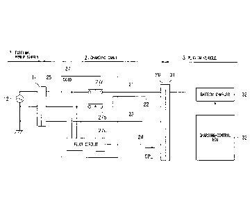
FIG. 1 is a schematic diagram illustrating the configuration of a vehicle
charging
system according to an embodiment of the invention. As shown in FIG. 1, the
vehicle
charging system according to this embodiment includes an external power supply
1, a
charging cable 2, and a plug-in vehicle 3. The external power supply 1
includes a
power receptacle 11 with a ground terminal disposed, for example, in a house
and an AC
power supply (commercial power supply) 12 supplying single-phase AC power to
the
power receptacle 11.
The charging cable 2 includes two power supply lines 21 and 22, a ground line
23, a pilot line 24, a plug 25, and a cable-side coupler 26, and a CCID 27. In
each of
the power supply lines 21 and 22 and the ground line 23, an end thereof is
connected to
the plug 25 and the other end thereof is connected to the cable-side coupler
26. An end
of the pilot line 24 is connected to the CCID 27 (specifically, a pilot
circuit 27c) and the
other end thereof is connected to the cable-side coupler 26.
By connecting the plug 25 to the power receptacle 11, one end of each of the
power supply lines 21 and 22 is connected to the AC power supply 12 and one
end of the
ground line 23 is connected to the ground of the external power supply 1. By
connecting the cable-side coupler 26 to a vehicle-side coupler 31 of the plug-
in vehicle 3,
the other end of each of the power supply lines 21 and 22 is connected to a
battery
charger 32 of the plug-in vehicle 3 and the other end of each of the ground
line 23 and
CA 02792870 2012-10-18
6
the pilot line 24 is connected to a charging-control ECU 33 of the plug-in
vehicle 1
The CCID 27 is a control unit that is disposed in the middle of the power
supply
lines 21 and 22 and the ground line 23, and includes relays 27a and 27b
disposed in the
middle of the power supply lines 21 and 22 and a pilot circuit 27c
transmitting a pilot
signal CPL to the charging-control ECU 33 of the plug-in vehicle 3 via the
pilot line 24
and controlling ON and OFF states of the relays 27a and 27b. The pilot circuit
27c is
connected to the power supply lines 21 and 22 and the ground line 23 and is
supplied
with a source voltage from the power supply lines 21 and 22 and with a ground
voltage
from the ground line 23.
The plug-in vehicle 3 is a vehicle which can be charged with the external
power
supply 1, such as an electric car or a plug-in hybrid car, and includes a
vehicle-side
coupler 31, a battery charger 32, and a charging-control ECU 33. By connecting
the
cable-side coupler 26 of the charging cable 2 to the vehicle-side coupler 31,
the power
supply lines 21 and 22 are connected to the battery charger 32, and the ground
line 23
and the pilot line 24 are connected to the charging-control ECU 33.
The battery charger 32 is a charging circuit that converts single-phase AC
power
supplied from the external power supply 1 via the charging cable 2 (the power
supply
lines 21 and 22) into DC power under the control of the charging-control ECU
33 and
that charges a driving battery (not shown) mounted on the plug-in vehicle 3
with the DC
power. The charging-control ECU 33 is an electronic control unit that receives
a pilot
signal CPL via the charging cable 2 before being supplied with the power when
the
plug-in vehicle 3 is connected to the external power supply 1 via the charging
cable 2 and
that performs a process necessary for the charging control of the driving
battery based on
the pilot signal CPL.
FIG. 2 is a diagram illustrating the internal configuration of the charging-
control
CA 02792870 2012-10-18
7
ECU 33. As shown in FIG. 2, the charging-control ECU 33 includes a pilot
signal input
terminal 100, an avalanche diode 101, a first diode 102, a first pull-down
resistor 103, a
pilot voltage setting circuit 104, an input circuit 105, a pseudo-signal
supply circuit 106,
and a CPU 107.
The pilot signal input terminal 100 is an external input terminal that is
connected
to the pilot line 24 when the cable-side coupler 26 of the charging cable 2 is
connected to
the vehicle-side coupler 31. The avalanche diode 101 has one end connected to
the
pilot signal input terminal 100 and the other end connected to the ground and
serves to
maintain the voltage of the pilot signal CPL (the voltage between the pilot
signal input
terminal 100 and the ground) input via the pilot signal input terminal 100 at
V1 (for
example, 12 V) or lower.
The first diode 102 has an anode terminal connected to the pilot signal input
terminal 100 and a cathode terminal connected to one end of the first pull-
down resistor
103 and serves to pass only a positive signal of the pilot signal CPL. The
first
pull-down resistor 103 has one end connected to the cathode terminal of the
first diode
102 and the other end connected to the ground and serves to change the
positive voltage
of the pilot signal CPL (that is, the voltage between the cathode terminal of
the first diode
102 and the ground) from Vito V2 (for example, 9 V).
The pilot voltage setting circuit 104 is a circuit that changes the positive
voltage
of the pilot signal CPL in a stepwise manner (for example, changes the voltage
from V2
to V3 (for example, 6 V)) under the control of the CPU 107 and includes a
second
pull-down resistor 104a and a first switching element 104b which is, for
example, an
npn-type transistor.
In the pilot voltage setting circuit 104, one end of the second pull-down
resistor
104a is connected to the cathode terminal of the first diode 102 and the other
end thereof
CA 02792870 2012-10-18
8
is connected to the collector terminal of the first switching element 104b.
The collector
terminal of the first switching element 104b is connected to the other end of
the first
pull-down resistor 104a, the emitter terminal thereof is connected to the
ground, and the
base terminal thereof is connected to a first control signal output port
CTI_OUT of the
CPU 107. The first switching element 104b is switched between ON and OFF
states
depending on a first control signal CT1 output from the first control signal
output port
CT I_OUT of the CPU 107 to the base terminal.
In the pilot voltage setting circuit 104 having this configuration, when the
first
switching element 104b is in ON state, the other end of the second pull-down
resistor
104a is connected to the ground and the positive voltage of the pilot signal
CPL is
changed from V2 to V3.
The input circuit 105 is disposed in a stage preceding the input port of the
CPU
107 and includes an input buffer 105a and a timer IC 105b. Here, the input
port of the
CPU 107 includes an interrupt port CPL_1NT used to input a start-up factor
interrupt
signal serving as a start-up factor of the CPU 107 and a duty measurement port
CPL_DUTY used to measure a duty ratio of the pilot signal CPL.
The input buffer 105a is, for example, a logic IC (NOT circuit), the input
terminal thereof is connected to the cathode terminal of the second diode 102,
and the
output terminal thereof is connected to the input terminal of the timer IC
105b and the
duty measurement port CPL DUTY of the CPU 107. The timer IC 105b includes an
input terminal connected to the output terminal of the input buffer 105a and
an output
terminal connected to the interrupt port CPL JNT of the CPU 107 and serves to
generate
the start-up factor interrupt signal and to output the generated start-up
factor interrupt
signal to the interrupt port CPL [NT when a pulse-like pilot signal CPL is
input.
In this way, the input circuit 105 is a circuit that generates the start-up
factor
CA 02792870 2012-10-18
9
interrupt signal and outputs the generated start-up factor interrupt signal to
the interrupt
port CPL_1NT of the CPU 107 and that buffers the pilot signal CPL and outputs
the
buffered pilot signal to the duty measurement port CPL DUTY of the CPU 107,
when a
pulse-like pilot signal CPL is input.
, 5 The pseudo-signal supply circuit 106 is a circuit that supplies a
pseudo-pilot
signal to the pilot signal line L extending from the pilot signal input
terminal 100 to the
input circuit 105 under the control of the CPU 107 and includes a second
switching
element 106a which is, for example, a pnp-type transistor, a second diode
106b, and two
resistors 106c and 106d.
The emitter terminal of the second switching element 106a is connected to a
power supply line PL1, the collector terminal thereof is connected to the
pilot signal line
L via the second diode 106b, and the base terminal thereof is connected to a
second
control signal output port CT2_OUT of the CPU 107 via the resistor 106c. The
second
switching element 106a is switched between ON and OFF states depending on a
second
control signal CT2 output from the second control signal output port CT2_OUT
of the
CPU 107 to the base terminal thereof.
The charging-control ECU 33 includes a regulator that drops a main source
voltage \imp supplied from a low-voltage battery mounted on the plug-in
vehicle 3
independently of a driving battery to generate a sub source voltage VREG. The
sub
source voltage VREG output from the regulator is applied to the power supply
line PL I .
The anode terminal of the second diode 106b is connected to the collector
terminal of the second switching element 106a and the cathode terminal thereof
is
connected to the pilot signal line L. One end of the resistor 106c is
connected to the
base terminal of the second switching element 106a and the other end thereof
is
connected to the second control signal output port CT2_OUT of the CPU 107. One
end
CA 02792870 2012-10-18
of the resistor 106d is connected to the emitter terminal of the second
switching element
106a and the other end thereof is connected to the other end of the resistor
106c.
In the pseudo-signal supply circuit 106 having this configuration, it is
possible
to supply a pulse signal of a desired frequency and a desired duty ratio as a
pseudo-pilot
5 signal to the pilot signal line L by controlling the second switching
element 106a in a
PWM manner. The maximum amplitude value of the pseudo-pilot signal is equal to
the
sub source voltage VREG.
The CPU 107 is a processor that performs a process necessary for a charging
control based on the pilot signal CPL (in other words, based on the signal
states of the
10 interrupt port CPL_INT and the duty measurement port CPL DUTY) and that
controls
the pilot voltage setting circuit 104 to change the voltage of the pilot
signal CPL in a
stepwise manner.
Although the details will be described later, the CPU 107 has a function of
performing a malfunction diagnosis for the input circuit 105 based on the
signal states of
the interrupt port CPL_INT and the duty measurement port CPL_DUTY when
controlling the pseudo-signal supply circuit 106 to supply a pulse-like pseudo-
pilot signal
to the pilot signal line L as the malfunction diagnosis process for the input
circuit 105.
The operation of the vehicle charging system having the above-mentioned
configuration will be described below with reference to the timing diagram of
FIG. 3.
First, at time ti in FIG 3, when the plug 25 of the charging cable 2 is
connected
to the power receptacle 11 of the external power supply I, the pilot circuit
27c of the
CCID 27 is supplied with power from the AC power supply 12 via the power
supply lines
21 and 22, is started up, and outputs a pilot signal CPL of a voltage value V1
(12 V) via
the pilot line 24. At this time point, the relays 27a and 27b of the CCID 27
are in OFF
state and the CPU 107 of the charging-control ECU 33 is in a sleep state.
CA 02792870 2012-10-18
11
As shown in FIG. 3, when the CPU 107 is in the sleep state, the first control
signal CT1 output from the CPU 107 is at a low level. Accordingly, the first
switching
element 104b of the pilot voltage setting circuit 104 is in OFF state. At this
time point,
since the pilot signal CPL is not input to the charging-control ECU 33, the
start-up factor
interrupt signal output from the timer IC 105b of the input circuit 105 is at
a low level
and the signal state of the interrupt port CPL_INT of the CPU 107 is also at a
low level.
Subsequently, at time t2 in FIG 3, when the cable-side coupler 26 of the
charging cable 2 is connected to the vehicle-side coupler 31 of the plug-in
vehicle 3, the
pilot signal CPL is input to the pilot signal input terminal 100 of the
charging-control
ECU 33, but the positive voltage of the pilot signal CPL (the voltage between
the cathode
terminal of the first diode 102 and the ground) is changed from Vito V2 (9 V)
by the
first pull-down resistor 103.
When the change in voltage of the pilot signal CPL (the change in voltage of
the
pilot line 24) is detected, the pilot circuit 27c of the CCID 27 determines
that the
charging cable 2 is connected to the plug-in vehicle 3 and informs the
charging-control
ECU 33 of the rated current of the power supply facility by transmitting the
pilot signal
CPL at a duty ratio corresponding to the rated current of the power supply
facility (the
external power supply 1 and the charging cable 2) at time t3 in FIG. 3.
In this way, after time t3, when the pulse-like pilot signal CPL having a duty
ratio corresponding to the rated current is input to the charging-control ECU
33, the timer
IC 105b of the input circuit 105 outputs a start-up factor interrupt signal of
a high level to
the interrupt port CPL_INT of the CPU 107 at time t4 in a fixed time td after
detecting a
first edge of the pulse-like pilot signal CPL. That is, at time t4, the signal
state of the
interrupt port CPL_INT is changed to a high level.
When the CPU 107 detects at time t4 that the signal state of the interrupt
port
CA 02792870 2012-10-18
12
CPL INT is changed to a high level, the CPU 107 is started up from the sleep
state and
measures the duty ratio of the pilot signal CPL based on the signal state of
the duty
measurement port CPL_DUTY (that is the output signal of the input buffer 105a)
to
acquire the rated current of the power supply facility. Then, the CPU 107
outputs the
first control signal CT1 of a high level at time t5 in FIG 3 to switch the
first switching
element 104b to ON state and changes the voltage of the pilot signal CPL from
V2 to V3
(6 V), whereby the COD 27 of the charging cable 2 is informed of the
completion of the
preparation for charging.
When the pilot circuit 27c of the CCID 27 detects that the voltage of the
pilot
signal CPL (the voltage of the pilot line 24) is changed from V2 to V3, the
pilot circuit
27c determines that the preparation for charging of the plug-in vehicle 3 is
completed,
and turns on the relays 27a and 27b for supplying the AC power of the external
power
supply 1 to the plug-in vehicle 3 (that is, starts the supply of power).
Accordingly, the
AC power is supplied from the external power supply 1 to the battery charger
32 of the
.. plug-in vehicle 3 via the charging cable 2 (the power supply lines 21 and
22).
The CPU 107 of the charging-control ECU 33 appropriately controls the
charging of the driving battery by controlling the battery charger 32 based on
the rated
current of the power supply facility acquired from the duty ratio of the pilot
signal CPL.
In this way, in the charging-control ECU 33, the input circuit 105 plays an
.. important role in acquiring the rated current of the power supply facility
by starting up
the CPU 107. When the input circuit 105 is out of order, the CPU 107 may not
be
started up or the rated current of the power supply facility may not be
acquired, whereby
an appropriate charging control cannot be performed.
Therefore, it is important to perform a malfunction diagnosis for the input
circuit
.. 105. In this embodiment, the CPU 107 of the charging-control ECU 33
performs the
CA 02792870 2012-10-18
13
malfunction diagnosis process for the input circuit 105 in accordance with the
following
sequence. Two examples of the malfunction diagnosis process will be described
below,
and any malfunction diagnosis process may be employed. The CPU 107 performs
the
following malfunction diagnosis process when the charging cable 2 is not
connected to
the plug-in vehicle 3 (for example, when the plug-in vehicle 3 is traveling).
This is
because the above-mentioned charging operation is interrupted when the
malfunction
diagnosis process is performed in a state where the charging cable 2 is
connected to the
plug-in vehicle 3.
A first example of the malfunction diagnosis process performed by the CPU 107
will be described below with reference to the timing diagram of FIG 4A.
First, the CPU 107 controls the first switching element 104b and the second
switching element 106a into OFF state by setting the first control signal CT1
to a low
level and setting the second control signal CT2 to a high level as an initial
process. At
this time, since the signal state of the interrupt port CPL_INT of the CPU 107
is at a low
level.
Subsequently, the CPU 107 controls the second switching element 106a in a
PWM manner by outputting the pulse-like second control signal CT2 with a fixed
frequency (for example, 1 kHz with a duty ratio of, for example, 50%) in the
period of
times ti 1 to t13 in FIG 4A. Accordingly, in the period of times tll to t13, a
pulse-like
pseudo-pilot signal having the same frequency and duty ratio as the second
control signal
CT2 is supplied from the pseudo-signal supply circuit 106 to the pilot signal
line L.
The timer IC 105b of the input circuit 105 sets the start-up factor interrupt
signal
to a high level at time t12 in a fixed time td after detecting a first edge of
the pseudo-pilot
signal at time tll, and sets the start-up factor interrupt signal to a low
level at time t14 in
a fixed time td after detecting a final edge of the pseudo-pilot signal at
time t13. That is,
CA 02792870 2012-10-18
14
the signal state of the interrupt port CPL_INT of the CPU 107 is at a high
level only in
the period of times t12 to t14.
The CPU 107 performs the malfunction diagnosis for the input circuit 105 based
on the signal state of the interrupt port CPL INT when controlling the pseudo-
signal
supply circuit 106 to supply the pulse-like pseudo-pilot signal to the pilot
signal line L as
described above. Specifically, the CPU 107 determines that the input circuit
105 is
normal, when the signal state of the interrupt port CPL_INT is changed to a
high level in
a fixed time td after starting the supply of the pseudo-pilot signal and the
signal state of
the interrupt port CPL_INT is changed to a low level in a fixed time td after
stopping the
supply of the pseudo-pilot signal.
The CPU 107 determines that the input circuit 105 malfunctions, when the
signal state of the interrupt port CPL_INT is not changed from a low level to
a high level
even in a fixed time td after starting the supply of the pseudo-pilot signal
or when the
signal state of the interrupt port CPL_INT is not changed from a high level to
a low level
even in a fixed time td after stopping the supply of the pseudo-pilot signal.
A second example of the malfunction diagnosis process performed by the CPU
107 will be described below with reference to the timing diagram of FIG. 4B.
First, the CPU 107 controls the first switching element 104b into ON state and
controls the second switching element 106a into OFF state, by setting the
first control
signal CT1 and the second control signal CT2 to a high level as an initial
process. At
this time, since the signal state of the interrupt port CPL_INT of the CPU 107
is at a low
level.
Subsequently, the CPU 107 controls the second switching element 106a in a
PWM manner by outputting the pulse-like second control signal CT2 with a fixed
frequency (for example, 500 Hz with a duty ratio of, for example, 50%) in the
period of
CA 02792870 2012-10-18
times t21 to t23 in FIG 4B. Accordingly, in the period of times t21 to t23, a
pulse-like
pseudo-pilot signal having the same frequency and duty ratio as the second
control signal
CT2 is supplied from the pseudo-signal supply circuit 106 to the pilot signal
line L.
The CPU 107 switches the first switching element 104b to OFF state at time
t23.
5 The timer IC 105b of the input circuit 105 sets the start-up factor
interrupt signal
to a high level at time t22 in a fixed time td after detecting the first edge
of the
pseudo-pilot signal at time t21, and sets the start-up factor interrupt signal
to a low level
at time 124 in a fixed time td after detecting the final edge of the pseudo-
pilot signal at
time 123. That is, the signal state of the interrupt port CPL_INT of the CPU
107 is at a
10 high level only in the period of times 122 to t24.
In the period of times 121 to 123, since a pulse signal having the same
frequency
and duty ratio as the pseudo-pilot signal is output from the input buffer 105a
to the duty
measurement port CPL_DUTY of the CPU 107, the signal state of the duty
measurement
port CPL_DUTY is changed to the same frequency and duty ratio as the pseudo-
pilot
15 signal.
The CPU 107 performs the malfunction diagnosis for the input circuit 105 based
on the signal states of the interrupt port CPL_INT and the duty measurement
port
CPL_DUTY when controlling the pseudo-signal supply circuit 106 to supply the
pulse-like pseudo-pilot signal to the pilot signal line L. Specifically, the
CPU 107
determines that the input buffer 105a and the timer IC 105b in the input
circuit 105 are
normal, when it can be detected that an edge is generated in the signal state
of the
interrupt port CPL_INT in a fixed time td after starting the supply of the
pseudo-pilot
signal and in a fixed time td after stopping the supply of the pseudo-pilot
signal.
The CPU 107 determines that the line extending from the input buffer 105a of
the input circuit 105 to the duty measurement port CPL_DUTY is normal, when it
can be
CA 02792870 2012-10-18
16
detected that an edge is generated in the signal state of the duty measurement
port
CPL_DUTY after starting the supply of the pseudo-pilot signal.
On the other hand, the CPU 107 determines that the input buffer 105a and the
timer IC 105b in the input circuit 105 malfunction, when it cannot be detected
that an
edge is generated in the signal state of the interrupt port CPL INT or when
edges are
detected but the edge detection times are different.
The CPU 107 determines that the line extending from the input buffer 105a of
the input circuit 105 to the duty measurement port CPL_DUTY malfunction (it is
supposed that the input buffer 105a malfunctions or the line is disconnected),
when it
cannot be detected that an edge is generated in the signal state of the duty
measurement
port CPL_DUTY or when edges are detected but a large difference exists for the
frequency and the duty ratio of the pseudo-pilot signal.
As described above, according to this embodiment, since the pseudo-signal
supply circuit 106 supplying the pseudo-pilot signal is disposed in the pilot
signal line L
extending from the pilot signal input terminal 100 of the charging-control ECU
33 to the
input circuit 105, it is possible to perform the malfunction diagnosis for the
input circuit
105 based on the signal state of the input port of the CPU 107 when
controlling the
pseudo-signal supply circuit 106 to supply the pseudo-pilot signal to the
pilot signal line
L.
The invention is not limited to the above-mentioned embodiment, but may be
modified as follows.
For example, the above-mentioned embodiment employs the configuration in
which the voltage of the pilot signal CPL is automatically changed from Vito
V2 at the
time point (at time t2 in FIG. 3) at which the charging cable 2 is connected
to the plug-in
vehicle 3. However, the invention is not limited to this configuration, and
may employ
CA 02792870 2012-10-18
17
a configuration in which the CPU 107 is started up at the time at which the
charging
cable 2 is connected to the plug-in vehicle 3, that is, when the pilot signal
CPL of a
voltage value V1 is input to the charging-control ECU 33, and the voltage of
the pilot
signal CPL is changed from Vito V2 under the control of the CPU 107.