Note: Descriptions are shown in the official language in which they were submitted.
CA 02793103 2014-08-13
Method for Controlled Shutdown of an Implantable Medical Device
1001] [Blank]
FIELD OF THE INVENTION
[002] The present invention relates to improved emergency shutdown circuitry
for an
implantable medical device
BACKGROUND
[003] Implantable stimulation devices are devices that generate and deliver
electrical stimuli to
body nerves and tissues for the therapy of various biological disorders, such
as pacemakers to
treat cardiac arrhythmia, defibrillators to treat cardiac fibrillation,
cochlear stimulators to treat
deafness, retinal stimulators to treat blindness, muscle stimulators to
produce coordinated limb
movement, spinal cord stimulators to treat chronic pain, cortical and deep
brain stimulators to
treat motor and psychological disorders, and other neural stimulators to treat
urinary
incontinence, sleep apnea, shoulder sublaxation, etc. The description that
follows will generally
focus on the use of the invention within a Spinal Cord Stimulation (SCS)
system, such as that
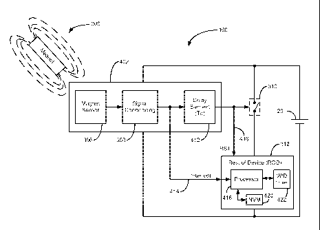
disclosed in U.S. Patent 6,516,227. However, the present invention may find
applicability in any
implantable medical device system.
[004] As shown in Figures IA and 1B, a SCS system typically includes an
Implantable Pulse
Generator (IPG) 100, which includes a biocompatible device case 30 formed of a
conductive
material such as titanium for example. The case 30 typically holds the
circuitry and battery 26
necessary for the IPG to function, although IPGs can also be powered via
external RF energy and
without a battery. The IPG 100 is coupled to electrodes 106 via one or more
electrode leads (two
such leads 102 and 104 are shown), such that the electrodes 106 form an
electrode array 110.
The electrodes 106 are carried on a flexible body 108, which also houses the
individual signal
wires 112 and 114 coupled to each electrode. In the illustrated embodiment,
there are eight
electrodes on lead 102, labeled E1-E8, and eight electrodes on lead 104,
labeled E9-E16, although
1
CA 02793103 2012-09-13
WO 2011/119276 PCT/US2011/025463
the number of leads and electrodes is application specific and therefore can
vary. The leads 102,
104 couple to the IPG 100 using lead connectors 38a and 38b, which are fixed
in a non-
conductive header material 36, which can comprise an epoxy for example.
[005] As shown in Figure 2, the IPG 100 typically includes an electronic
substrate assembly 14
including a printed circuit board (PCB) 16, along with various electronic
components 20, such as
microprocessors, integrated circuits, and capacitors mounted to the PCB 16.
Two coils (more
generally, antennas) are generally present in the IPG 100: a telemetry coil 13
used to
transmit/receive data to/from an external controller 12; and a charging coil
18 for charging or
recharging the IPG's battery 26 using an external charger 50. The telemetry
coil 13 is typically
mounted within the header 36 of the IPG 100 as shown, and may be wrapped
around a ferrite
core 13'.
[006] As just noted, an external controller 12, such as a hand-held programmer
or a clinician's
programmer, is used to wirelessly send data to and receive data from the IPG
100. For example,
the external controller 12 can send programming data to the IPG 100 to dictate
the therapy the
IPG 100 will provide to the patient. Also, the external controller 12 can act
as a receiver of data
from the IPG 100, such as various data reporting on the IPG's status. The
external controller 12,
like the IPG 100, also contains a PCB 70 on which electronic components 72 are
placed to
control operation of the external controller 12. A user interface 74 similar
to that used for a
computer, cell phone, or other hand held electronic device, and including
touchable buttons and a
display for example, allows a patient or clinician to operate the external
controller 12. The
communication of data to and from the external controller 12 is enabled by a
coil (antenna) 17.
[007] The external charger 50, also typically a hand-held device, is used to
wirelessly convey
power to the IPG 100, which power can be used to recharge the IPG's battery
26. The transfer of
power from the external charger 50 is enabled by a coil (antenna) 17'. For the
purpose of the
basic explanation here, the external charger 50 is depicted as having a
similar construction to the
external controller 12, but in reality they will differ in accordance with
their functionalities as
one skilled in the art will appreciate.
[008] Wireless data telemetry and power transfer between the external devices
12 and 50 and the
IPG 100 takes place via inductive coupling, and specifically magnetic
inductive coupling. To
implement such functionality, both the IPG 100 and the external devices 12 and
50 have coils
which act together as a pair. In case of the external controller 12, the
relevant pair of coils
2
CA 02793103 2012-09-13
WO 2011/119276 PCT/US2011/025463
comprises coil 17 from the controller and coil 13 from the IPG 100. In case of
the external
charger 50, the relevant pair of coils comprises coil 17' from the charger and
coil 18 from the
IPG 100.
[009] When data is to be sent from the external controller 12 to the IPG 100
for example, coil 17
is energized with an alternating current (AC). Such energizing of the coil 17
to transfer data can
occur using a Frequency Shift Keying (FSK) protocol for example, such as
disclosed in U.S.
Patent Publication 2009/0024179. Energizing the coil 17 produces a magnetic
field, which in
turn induces a voltage in the IPG's coil 13, which produces a corresponding
current signal when
provided a closed loop path. This voltage and/or current signal can then be
demodulated to
recover the original data. Transmitting data from the IPG 100 to the external
controller 12
occurs in essentially the same manner.
[0010] When power is to be transmitted from the external charger 50 to the IPG
100, coil 17' is
again energized with an alternating current. Such energizing is generally of a
constant
frequency, and may be of a larger magnitude than that used during the transfer
of data, but
otherwise the basic physics involved are similar.
[0011] The IPG 100 can also communicate data back to the external charger 50
by modulating
the impedance of the charging coil 18. This change in impedance is reflected
back to coil 17' in
the external charger 50, which demodulates the reflection to recover the
transmitted data. This
means of transmitting data from the IPG 100 to the external charger 50 is
known as Load Shift
Keying (LSK), and is useful to communicate data relevant during charging of
the battery 26 in
the IPG 100, such as the capacity of the battery, whether charging is complete
and the external
charger can cease, and other pertinent charging variables. LSK communication
from an IPG 100
to an external charger is discussed further in U.S. Patent Publication
2010/0179618.
[0012] As is well known, inductive transmission of data or power can occur
transcutaneously,
i.e., through the patient's tissue 25, making it particularly useful in a
medical implantable device
system. During the transmission of data or power, the coils 17 and 13, or 17'
and 18, preferably
lie in planes that are parallel, along collinear axes, and with the coils as
close as possible to each
other. Such an orientation between the coils 17 and 13 will generally improve
the coupling
between them, but deviation from ideal orientations can still result in
suitably reliable data or
power transfer.
[0013] IPG 100 can comprise circuitry that enables a user or a clinician to
shutdown the IPG 100
3
CA 02793103 2012-09-13
WO 2011/119276 PCT/US2011/025463
in case of emergencies. Such emergencies can arise when the IPG 100
malfunctions, undesirably
over-stimulates the patient, does not provide stimulation at all, etc. Figure
3 shows circuitry 302
that is traditionally used in the IPG 100 for emergency shutdown. A user or
clinician brings a
magnet 300 near the location on the patient's body where the IPG 100 is
situated. A magnet
sensor 306, such as a reed switch, detects the presence of magnet 300 by way
of sensing its
magnetic field, and sends an electrical signal (voltage or current) to a
signal conditioning circuit
308. The signal conditioning circuit 308 suppresses any stray and transient
signals (e.g., reed
bounce) received from the magnet sensor 306. Once a sufficient signal
indicating presence of
magnet 300 is detected, the signal conditioning circuit 308 outputs a signal
that opens switch
310. Once switch 310 is open, Rest of the Device (ROD) 312 will be
disconnected from battery
26. ROD 312 will typically include all the circuitry responsible for the
functioning of the IPG
100. For example, ROD 312 can include the microprocessor, charging circuits,
telemetry
circuits, stimulation circuits, volatile and non-volatile memory, etc. Upon
being disconnected
from the battery, these circuits will cease to function.
[0014] Although the aim of an emergency stop may be to immediately halt any
stimulation being
received by the IPG 100, an abrupt shut down like the one depicted in Figure
3, can have certain
disadvantages. For example, any data stored in volatile memory (e.g., RAM)
will be lost, which
data may include current stimulation program parameters. If the current
stimulation parameters
were intended to be stored/saved in non-volatile memory (into a stimulation
parameter file, for
example), an abrupt power loss may prevent the microprocessor from completing
the save
operation. In other instances it is also possible that the microprocessor is
in the process of
moving data from volatile memory to non-volatile memory when power loss
occurs. This may
result in only a partial data store¨possibly corrupting the data stored in non-
volatile memory.
[0015] In other instances it may be beneficial, from an analysis point of
view, to record data
relevant to the emergency shutdown itself. However, an abrupt shutdown may not
allow the
microprocessor to log this information into non-volatile memory.
[0016] A solution to this problem is provided in this disclosure in the form
of an improved
emergency shutdown circuit for an IPG 100 or other implantable medical device.
4
CA 02793103 2012-09-13
WO 2011/119276 PCT/US2011/025463
BRIEF DESCRIPTION OF THE DRAWINGS
[0017] Figures lA and 1B show an implantable medical device, and the manner in
which an
electrode array is coupled to the IPG in accordance with the prior art.
[0018] Figure 2 shows the relation between the implantable medical device, an
external
controller, and an external charger.
[0019] Figure 3 shows a traditional emergency IPG shutdown circuit in an IPG.
[0020] Figure 4 shows a first embodiment of improved emergency shutdown
circuitry for the
IPG of Figure 3 to provide graceful shutdown.
[0021] Figure 5 shows a detailed exemplary circuit diagram of the emergency
shutdown circuitry
of Figure 4.
[0022] Figures 6A-6D show timing diagrams of various signals of the circuits
shown in Figures
4 and 5.
[0023] Figure 7 shows a flowchart depicting shutdown operations performed by
the IPG.
DETAILED DESCRIPTION
[0024] The description that follows relates to use of the invention within a
spinal cord
stimulation (SCS) system. However, it is to be understood that the invention
is not so limited,
and could be used with any type of implantable medical device system.
[0025] The inventor addresses the problem of data loss during emergency
shutdown of the IPG
100 by including a delay element 412 between the signal conditioner 308 and
the switch 310 in
an improved emergency shutdown circuit 402, as shown in Figure 4. In contrast
with emergency
shutdown circuit 302 of Figure 3, where the output of the signal conditioning
circuit 308 is fed
directly to the power cut-off switch 310, the emergency shutdown circuit 402
in Figure 4 instead
delays the output of the signal conditioning circuit 308 before it is fed to
the power cut-off
switch 310. In addition, output of the signal conditioner 308 is provided as
an interrupt signal
414 to the ROD 312. As a result, as soon as the signal conditioning circuit
308 outputs signal
indicating that magnet 300 has been detected, ROD 312 receives a notification,
in the form of the
interrupt signal 414, of an imminent emergency shutdown. Interrupt signal 414
is fed to an
interrupt pin of processor 418, which can immediately launch a shutdown
routine (discussed
further below) that allows it to carry out shutdown operations such as logging
the emergency
shutdown event, saving and closing open files, etc. A timing delay (Td)
produced by delay
CA 02793103 2012-09-13
WO 2011/119276 PCT/US2011/025463
element 412 is selected to provide the processor 418 enough time to complete
the launched
shutdown routine, which time can vary between applications.
[0026] After the elapse of grace-period delay Td, the delay element 412
outputs signal 416.
Signal 416 is fed to the input of shutdown switch 310 and a reset pin RST of
the processor 418.
Upon receiving signal 416, switch 310 (which is normally closed) opens and, as
a result,
disconnects ROD 312 from battery 26. The emergency shutdown circuit 402,
comprising
magnet sensor 306, signal conditioning circuit 308, and the delay element 412,
is powered
separately from the ROD 312. Furthermore, emergency shutdown circuit 402 may
be
implemented on a separate substrate than the one on which ROD 312 is
implemented. This
reduces system faults that may occur in the ROD 312 from affecting the
emergency shutdown
circuit 402.
[0027] Figure 5 shows a detailed exemplary circuit diagram of emergency
shutdown circuit 402.
In default state¨when no magnetic field is sensed by the magnet sensor 306¨the
output of the
magnet sensor is pulled low by the pull down resistor Rpull down 521.
Therefore, the output 414 of
the signal conditioning circuit 308 is low. Note that the output 414 of the
signal conditioning
circuit 308 is coupled to an interrupt input of the processor (418, Figure 4).
It is assumed that the
processor 418 activates an interrupt routine only when the interrupt input of
the processor is at
logic high value. Therefore, in the default state, the processor is not
interrupted. Furthermore,
by virtue of inverters 531 and 534, the output 416 of the delay element 412 is
also logic low and
the capacitor 533 is fully charged. Therefore, shutdown switch 310 remains
closed, keeping
ROD 312 connected to battery 26. In other words, without the detection of an
emergency stop
by way of magnet 300, ROD 312 continues to receive power.
[0028] As stated before, when an emergency shutdown is needed, magnet 300 is
brought near the
IPG 100. Magnet sensor 306 senses the approach of magnet 300. Magnet 300 is
typically a
permanent magnet that produces a magnetic field that is considerably larger
than the earth's
magnetic field (-0.5 gauss). Magnet sensor 306 is preferably designed such
that it produces a
null output when placed in only the earth's magnetic field, but produces an
output when placed
in the magnetic field produced by magnet 300. Several types of magnetic field
sensors 306 can
be used, for example, reed switches, InSb magnetoresistors, Hall devices, GMR
sensors, etc.
[0029] As an example, Figure 5 shows a reed switch 512 being used as magnet
sensor 306. One
end of the reed switch 512 is connected to the supply voltage Vbat, while the
other end is
6
CA 02793103 2012-09-13
WO 2011/119276 PCT/US2011/025463
connected to pull down resistor Rpull down 521. The pull down resistor Rpull
down 521 maintains the
voltage at the output of the magnet sensor 306 to a voltage that is
approximately equal to GND.
The reed switch 512 includes a pair of flexible, ferromagnetic contacts, which
get magnetized by
the presence of the magnetic field of magnet 300. This magnetization causes
the contacts to
attract each other and close the circuit. This results in the output of the
magnet sensor 306 to be
pulled high.
[0030] It is not unusual for the output of the magnetic sensor 306 to toggle
or fluctuate between
high and low values. This can be caused due to reed bounce within the reed
switch 512, or by
erratic movement of the magnet 300. Fluctuations can also be caused by magnets
other than
magnet 300, such as magnets in DC motors and other electrical devices that the
patient may
commonly encounter in close proximity around the house or workplace. It is not
desired that
such fluctuations be interpreted as an actual emergency shutdown condition.
Therefore, a low
pass filter, formed by resistor Rf 522 and capacitor Cf 523, within the signal
conditioning circuit
308 is connected to the output of the magnet sensor 306, which low pass filter
filters the output
of the magnet sensor 306 before it is fed to inverter 525. The frequency
response of the low pass
filter can be adjusted by the values of Rf and Cf. Although a passive filter
formed by resistor Rf
522 and capacitor Cf 523 has been shown in Figure 5, a person skilled in the
art will appreciate
that active filters designed using components such as transistors, operational
amplifiers, etc., can
also be used.
[0031] Inverter 525, Schmitt trigger 526, and buffer 527 digitize the filtered
output of the magnet
sensor 306. Once the filtered output of the magnet sensor 306 reaches a
sufficiently high value,
the output of the inverter 525 goes low. The input to inverter 525, i.e., the
output of magnet
sensor 306, may transition from low to high relatively slowly by virtue of the
passive filter. This
can cause excessive current draw through the inverter 525, which is typically
(but not
necessarily) implemented using CMOS technology. In particular, the "crowbar
current"
experienced during a CMOS logic state transition can be exacerbated by the
filter. To limit this
crowbar current, a current source 524 is placed in series with the supply
voltage (Vbat) of the
inverter 525.
[0032] Output of the inverter 525 is fed to an inverting Schmitt trigger 526,
which will quickly
transition from low to high even if the output of the inverter 525 changes
from high to low
relatively slowly. The output of the Schmitt trigger 526 is fed to the input
of buffer 527, which
7
CA 02793103 2012-09-13
WO 2011/119276 PCT/US2011/025463
follows the input to the trigger 526. The operation of signal condition
circuit 308 can be seen in
Figures 6A and 6B, which respectively show the unfiltered output of the magnet
sensor 306, and
the digitized output of the signal condition circuit 308. Time Tõ denotes the
time taken from the
moment the magnet 300 is first sensed by the magnet sensor 306 to the moment
the output of
signal condition circuit 308 goes high, and essentially represents the time
taken to appropriate
condition the signal. Tõ would normally be significantly less than the grace-
period delay Td, and
may be included as part of the grace period delay.
[0033] Output of signal conditioning circuit 308 is fed to two locations¨as an
interrupt signal
414 to processor 418 and to the delay element 412. The interrupt 414 to the
processor 418 starts
an interrupt service routine within the processor 418 that carries out
controlled shutdown of the
IPG 100. The delay element 412 delays the output from the signal conditioning
circuit 308 from
opening switch 310 by an amount Td, which is designed to provide the processor
418 sufficient
time to carry out the required shutdown operations. The shutdown operation of
the processor
418 is described with further detail below with respect to Figure 7.
[0034] The delay element 412 includes inverter 531, delay capacitor 533, and
inverter 534.
When input of inverter 531, which is connected to the output of signal
conditioning circuit 308,
changes from low to high, the output of inverter 531, changes from high to
low. Note that in
default state (with no emergency shutdown) the delay capacitor 533 is fully
charged to a high
state. Therefore, the charge stored in the delay capacitor is drained to
ground GND via the n-
MOS transistor (not shown) of inverter 531 and current source 532. The amount
of time it takes
for the output of the inverter 531 to go from high to low depends upon the
amount of time it
takes to discharge delay capacitor 533, which time depends upon the size of
delay capacitor 533,
the size of the n-MOS transistor of the inverter 531 and the value of the
current source 532.
Having a small size n-MOS transistor and a small value of current source 532
can increase the
time it takes to discharge capacitor. Discharge time can also be increased by
increasing the size
of the delay capacitor 533. When the output of the inverter 531 begins to
change from high to
low, the output of the inverter 534 begins to change from low to high. In case
of inverter 534,
capacitance at the output of the inverter 534 is charged via the p-MOS
transistor (not shown) of
the inverter 534 and current source 535. Capacitance at the output of inverter
534 will
predominantly be interconnect capacitance. The amount of time required to
charge this
interconnect capacitance depends upon the value of the current source 535 and
the size of the p-
8
CA 02793103 2012-09-13
WO 2011/119276 PCT/US2011/025463
MOS transistor of inverter 534. Decreasing the value of the current source 535
can increase the
discharge time. Similarly, decreasing the size of the p-MOS transistor will
increase the
discharge time. In any event, these various values set the total delay Td
offered by the delay
element 412. After delay Td, the output of the delay element 412 goes high as
shown in Figure
6C. At this time, the shutdown switch 310 is opened, disconnecting the ROD 312
from the
battery 26.
[0035] As stated earlier, output of signal conditioning circuit 308 is fed as
an interrupt signal 414
to processor 418. Processor 418 may have one or more interrupt pins.
Preferably, the interrupt
signal 414 is connected to a non-maskable interrupt (NMI) pin of the processor
418 so that the
interrupt signal 414 is never ignored. Upon receiving an interrupt, the
processor 418 launches an
interrupt service routine (ISR), such as a shutdown routine, associated with
that interrupt pin,
which ISR is illustrated in Figure 7. This ISR carries out shutdown operations
such as logging
the emergency shutdown event, saving and closing open files, etc., before time
Td has lapsed,
i.e., before the ROD 312 is disconnected from its power supply.
[0036] In step 702, processor 418 refreshes a watch-dog timer 422 (Fig. 4).
The watch-dog timer
422 resets the processor 418 upon completion of a predetermined time interval,
and can be
implanted as a counter. For example, a down counter with initial count of FFFF
will reset the
processor 418 when it reaches 0000. Processor 418 periodically refreshes the
watch-dog timer
by resetting the counter before it reaches 0000. Non-servicing of the watch-
dog timer before it
reaches 0000 can serve as an indication of a fault condition or state.
Therefore, the resetting of
the processor 418 by the watch-dog timer 422 can bring the processor back to
normal operation.
In step 702, the processor resets the watch-dog timer 422 right at the outset
of the shutdown
routine so that the processor 418 can dedicate maximum available time in
carrying out shutdown
operations. Note that although the watch-dog timer 422 in Figure 4 is shown as
a separate entity
from the processor 418, it is not uncommon for processors 418 to include a
watch-dog timer 422.
[0037] In step 704 processor 418 stops any stimulation given to the patient,
i.e. ceases any
therapeutic operation being performed by the implantable medical device.
Alternatively,
operation of the implantable medical device may not cease entirely, but
instead may enter a
different mode safer for the patient. For example, in a neurostimulator,
initiation of the
shutdown routine may simply reduce the magnitude of the stimulation settings
to levels known to
be conservatively safe for even the most sensitive patient.
9
CA 02793103 2012-09-13
WO 2011/119276 PCT/US2011/025463
[0038] In step 706, processor 418 logs the emergency shutdown event in a log
file stored in non-
volatile memory 420 (Fig. 4). This includes various status data which can be
telemetered back to
the external controller 12 for further analysis. Such status data can include
operation parameters
such as current battery voltage, Vbat, stimulation status data, time stamps,
including the time
when the emergency shutdown event occurred, etc. The time stamps can be
derived from an
internal IPG clock (not shown). In some cases, the internal IPG clock may be
inaccurate,
although the technique disclosed in U.S. Patent Publication 2010/0125316 can
help in this
regard.
[0039] In step 708, processor 418 stops and closes any open or active
resources such as file
systems. This can entail closing log files, stimulation files that contain
stimulation data, or
system files required for the operation of the processor 418. By
systematically closing open or
active files, corruption or loss of data associated with an abrupt shutdown
can be reduced or
avoided. Closing files can also include saving data associated with the open
files into non-
volatile memory 420.
[0040] In step 710, processor 418 stores any remaining but required
information from volatile
memory (not shown in Fig. 4) to non-volatile memory 420. The processor 418
then enters a state
where it does not accept any additional commands (step 712). This is because
the external
controller 12 or an external charger 50 may be unaware that the IPG 100 is
undergoing an
emergency shutdown, and may continue to send commands and or instructions.
Because the IPG
100 is being prepared for shutdown, any such commands or instructions are
ignored. Processor
418 stays in step 712 until the delay time Td elapses and the processor 418
receives the reset RST
signal 416 from the delay element 412 (step 714), which signal also opens
switch 310 to
disconnect ROD 312 from the power supply (e.g., battery 26). As shown in
Figure 6D, at this
time, the power supply voltage at the ROD will begin to exponentially decay,
taking a time Tf to
complete, which time may be abrupt. However, because the ISR is designed to
have completed
during Td, the IPG 100 is unaffected by this fall off in the power supply
voltage.
[0041] In cases where the processor 418 has been rendered non-operational, the
processor 418
will be incapable of executing the shutdown routine described. In such cases,
the ROD 312 is
still disconnected from the power supply, and the reset RST signal 416 is
still given to the
processor 418 after delay Td.
CA 02793103 2014-08-13
100421 Magnet 300 can be removed from the proximity of the IPG 100 to allow
the IPG 100 to
return to normal operation. For example, when magnet 300 is moved away from
the IPG 100,
reed switch 512 will open and disconnect the output of the magnet sensor from
Vbat. As a result,
the output of the magnet sensor 306, and ultimately interrupt signal 414, are
both pulled low
indicating that an emergency shutdown state no longer exists. Note that at
this time the ROD
312 is still disconnected from the power supply. Once the interrupt signal 414
begins to
transition low, the reset signal 416 to the processor 418 will also go low and
switch 310 closed
after some delay through the delay element. (Note that the high-to-low
transition may be
differently delayed from the low-to-high transition delay of Td if the
circuitry within the delay
element 412 is not balanced). Processor 418 and the ROD 312 may then enter
initialization and
restore normal operation of the IPG 100.
[0043] Although the improved emergency shutdown circuitry is disclosed as
being activated
upon receipt of a magnetic field from a simple magnet, applications of the
technique are not so
limited. Instead, the sensor can generically sense any shutdown signal
wirelessly communicated
from any source external to the implantable medical device. For example, the
shutdown signal
may comprise a shutdown command telemetered to the sensor 306 from the
external controller
12 or external charger 50, with the sensor 306 in this case comprising a coil
or other antenna.
Even if such relatively-sophisticated means are used to signal the IPG to
shutdown, the improved
circuitry 402 can still operate to shutdown the IPG in a controlled and
graceful manner.
11