Note: Descriptions are shown in the official language in which they were submitted.
CA 02793377 2015-11-06
52966-77
MONITORING DEVICE AND A METHOD FOR WIRELESS DATA AND POWER
TRANSMISSION IN A MONITORING DEVICE
The present invention relates to monitoring devices. The invention more
specifically
relates to monitoring devices comprising a reader and a data carrier, adapted
for
wireless data and power transmission. The invention also relates to a method
for
operating a monitoring device.
BACKGROUND OF THE INVENTION
In the context of the present disclosure a monitoring device should be
understood as a
small device designed to be worn by a human user for continuous surveillance
of a
specific medical condition in the user. The monitoring device consists of a
reader and a
data carrier.
The reader is powered by an internal primary energy source, such as a battery.
The data
carrier does not have its own primary source of energy. Therefore the data
carrier relics
on a wireless inductive power transmission from the reader. A transmitter coil
in the
reader and a receiver coil in the data carrier together form a system of
magnetically
coupled inductors. The basic principle relies on generating an alternating
current in the
transmitter coil. The current in the transmitter coil generates a magnetic
field which
induces a current in the receiver coil. The current in the receiver coil is
used to power
the data carrier.
The data carrier has monitoring means, such as electrodes for measuring EEG
signals
in the human user of the monitoring device. The data collected by the
monitoring
means are preprocessed by data processing means and wirelessly transmitted to
the
reader for further processing. The reader receives data from the data carrier
through
load modulation of the data carrier. In a typical application the further
processing in the
reader includes determining if a specific medical condition has occurred in
the user and
alerting the user of this condition. Hereby the size and power consumption of
the data
carrier can be kept small because the battery and the main part of the signal
processing
is placed in the reader. This may make the data carrier feasible for
implantation in the
human user. It may be especially advantageous to have the data carrier
subcutaneously
implanted with respect to measurement of EEG signals.
CA 02793377 2014-10-24
, 52966-77
,
2
US-A-5260701 discloses a device for the bi-directional transmission of data
between a master
system and a slave system that uses a single transmission antenna and a single
reception
antenna, wherein the slave system comprises a switching circuit connected in
series between a
rectifier circuit and a power supply circuit to modulate the real part of the
impedance of the
slave system between a high value and a low value when the switching circuit
is driven in its
opened and closed position by a control signal representative of the data to
be transmitted to
the master system.
US-B1-6301138 discloses a data carrier with load modulation means and with
improved
power supply in the process of load modulation. Additional means secure that
the supply
voltage for the data processing means during load modulation can be kept at
least at the level
of the load modulation during the load modulation pauses. The disclosed
additional means
includes a voltage multiplier circuit and a charge pump.
SUMMARY OF THE INVENTION
An aspect of the present disclosure is directed to providing a monitoring
device incorporating
a reader and a data carrier with improved means for data transmission and
energy efficiency,
hereby providing a monitoring device with a reduced power consumption.
Another aspect of the present disclosure is directed to providing an improved
method for
operating a monitoring device.
The invention, in a first aspect, provides a monitoring device comprising a
reader and a data
carrier, adapted for wireless data transmission, from the data carrier to the
reader, using load
modulation and for powering the data carrier using a wireless inductive power
transmission
from the reader and to the data carrier, wherein the data carrier comprises a
receiver coil, data
processing means, rectifier means, switch means and at least two capacitors,
wherein the data
processing means, switch means and capacitors are connected such that, in a
first
configuration, the capacitors are coupled in parallel and, in a second
configuration, the
capacitors are coupled in series, whereby load modulation of the data carrier
is achieved by
switching between said first and second configuration, and said capacitors are
further arranged
CA 02793377 2014-10-24
52966-77
2a
for storing energy received from the wireless inductive power transmission and
for powering
the data processing means.
Based on this arrangement, some embodiments may provide a monitoring device
with a
reduced power consumption.
The invention, in a second aspect, provides a method of operating a data
carrier in a
monitoring device comprising the steps of providing in the data carrier a
first capacitor, a
second capacitor, switching means and data processing means, connecting the
first capacitor,
second capacitor, switching means and data processing means, and operating the
switching
means to obtain a first configuration, wherein the capacitors are connected in
parallel,
operating the switching means to obtain a second configuration, wherein the
capacitors are
connected in series, storing energy in the capacitors using energy received
from a wireless
inductive power transmission, powering the data processing means on the data
carrier, using
the stored energy, and switching between the two configurations in time with a
data stream to
be transmitted from the data carrier.
Based on this method, some embodiments may provide a method of operating a
monitoring
device with a reduced power consumption.
Other features of some embodiments of the present invention will become
apparent to those
skilled in the art from the following description wherein embodiments of the
invention will be
explained in greater detail.
=
CA 02793377 2012-09-17
WO 2011/124251 PCT/EP2010/054534
3
BRIEF DESCRIPTION OF THE DRAWINGS
By way of example, there is shown and described a preferred embodiment of this
invention. As will be realized, the invention is capable of other embodiments,
and its
several details are capable of modification in various, obvious aspects all
without
departing from the invention. Accordingly, the drawings and descriptions will
be
regarded as illustrative in nature and not as restrictive. In the drawings:
Fig. 1 illustrates an equivalent circuit diagram of a prior art data carrier
in a first state
of operation,
Fig. 2 illustrates an equivalent circuit diagram of the prior art data carrier
of fig. 1 in
a second state of operation,
Fig. 3 illustrates an equivalent circuit diagram of a data carrier, according
to a first
embodiment of the invention, in a first state of operation,
Fig. 4 illustrates an equivalent circuit diagram of the data carrier,
according to the
first embodiment of the invention, in a second state of operation,
Fig. 5 illustrates, in higher detail, the modulation portion of the data
carrier,
according to the first embodiment of the invention, in the first state of
operation,
Fig. 6 illustrates, in higher detail, the modulation portion of the data
carrier,
according to the first embodiment of the invention, in the second state of
operation,
Fig. 7 illustrates an equivalent circuit diagram of the data carrier,
according to a
second embodiment of the invention, in a second state of operation, and
Fig. 8 illustrates an equivalent diagram of a monitoring device incorporating
a reader
and a data carrier according to a third embodiment of the invention.
DETAILED DESCRIPTION
Reference is first made to Fig. 1, which illustrates an equivalent circuit
diagram of a
prior art data carrier. The data carrier is shown in a first state of
operation wherein the
data carrier is set primarily for receiving power wirelessly supplied from a
reader. The
circuit diagram comprises a receiver coil 101 and a resonance capacitor 102
that
CA 02793377 2012-09-17
WO 2011/124251 PCT/EP2010/054534
4
together form a resonant circuit that is tuned to a resonance frequency that
corresponds
to the transmission frequency of the wireless signal from the reader. The
circuit
diagram further comprises a rectifier 103, an energy storage capacitor 104, a
resistor
105 representing the load of the monitoring and data processing means on the
data
carrier, a switch 106, and a modulation resistor 107.
A small part of the wireless signal from the reader couples to the receiver
coil 101, and
induces a voltage across the receiver coil. The voltage is rectified in
rectifier 103, and
as a result energy is stored in the energy storage capacitor 104.
Reference is now made to Fig. 2, which illustrates an equivalent circuit
diagram of the
prior art data carrier of Fig. 1 in a second state of operation. In the first
state of
operation the switch 106 is open and in the second state the switch 106 is
closed. When
the switch 106 is closed the modulation resistor 107 is coupled in parallel
with the load
resistor 105.
A switching on and off of the modulation resistor 107 brings about a change in
impedance of the transmitter coil in the reader (to be described below) when
the reader
and data carrier are inductively coupled. This has the effect of an amplitude
modulation
of a voltage in the reader. Therefore data can be transmitted from data
carrier to reader
if the timing of the switching of the modulation resistor 107 is controlled by
the data to
be transmitted from the data carrier and to the reader. This type of load
modulation is
disadvantageous in that the voltage across the load resistor 105 may vary
during the
load modulation and in that power is dissipated as heat in the modulation
resistor 107.
Further details concerning prior art data carriers adapted for wireless power
supply and
wireless data transmission using load modulation of the data carrier can be
found in the
book by Klaus Finkenzeller: "RFID handbook: fundamentals and applications in
contactless smart cards and identification", John Wiley & Sons, (2003).
Reference is now made to Fig. 3 which illustrates an equivalent circuit
diagram of a
data carrier, according to a first embodiment of the invention. The rest of
the
monitoring device (i.e. the reader) is omitted from the drawing in order to
improve
clarity. The data carrier is shown in a first state of operation wherein the
data carrier is
set primarily for receiving power wirelessly supplied from a reader. The
circuit diagram
comprises a receiver coil 201, a resonance capacitor 202, a rectifier 203, an
energy
CA 02793377 2014-10-24
52966-77
storage capacitor 204, a resistor 205 representing the load of the monitoring
and data
processing means on the data carrier, a modulation capacitor 206 and
connection points
207 and 208.
Reference is now made to Fig. 4 which illustrates an equivalent circuit
diagram of the
5 data carrier of Fig. 3, according to the first embodiment of the
invention. The rest of the.
= monitoring device (i.e. the reader) is again omitted from the drawing in
order to
improve clarity. The data carrier is shown in a second state of operation
where the load .
of the data carrier, as seen from the reader, is changed relative to the first
state of
operation. The circuit diagram again comprises the receiver coil 201, the
resonance
capacitor 202, the rectifier 203, the energy storage capacitor 204, the
resistor 205
representing the load of the monitoring and data processing means on the data
carrier,
the modulation capacitor 206 and the connection points 207 and 208.
=
In the first state of operation the data carrier according to the first
embodiment of the
invention forms a low impedance resonant circuit, as seen from a reader
inductively
linked to the data carrier. In the second state of operation the data carrier
forms a high .
impedance resonant circuit. By switching between the two operating states in
time with =
a data stream to be transmitted from the data carrier and to the reader it
becomes
possible to reconstruct the data stream in the reader based on an appropriate
evaluation.
procedure in the reader.
It is a specific advantage of some embodiments of the present invention that
load modulation is =
achieved with only negligible power dissipation in the components used for the
load modulation.
According to an embodiment the capacitance of the energy storage capacitor 204
is -
between 2 and 10 times larger than the capacitance of the modulation capacitor
206 and
thercapacitance of the energy storage capacitor 204 is in the range between 5
and 20 nF,
while the capacitance of the modulation capacitor 206 is in the range between
0.5 and
10 nF. Preferably the capacitance of the energy storage capacitor is 10 nF and
the
capacitance of the modulation capacitor is 1 nF.
According to another embodiment the ratio of the capacitances of the
modulation
capacitor 206 and the energy storage capacitor 204 is in the range between 0.5
and 2. =
Preferably the capacitances of the two capacitors arc nominally identical and
in the
=
range between 0.5 nF and 20 nF.
=
=
CA 02793377 2015-11-06
52966-77
6
Reference is now made to Fig. 5 which illustrates the modulation portion of
the data carrier, in
higher detail, according to the first embodiment of the invention. Fig. 5
illustrates the energy
storage capacitor 204, the modulation capacitor 206, switches 209, 210 and 211
and connection
points 207 and 208. Fig. 5 illustrates the data carrier, when it is in the
first state of operation. In
this first state of operation the switches 209 and 211 are closed, and the
switch 210 is open. The
capacitors 204 and 206 are thus connected in parallel relative to the
connection points 207 and
208.
Reference is now made to Fig. 6 which illustrates the modulation portion of
the data carrier, in
higher detail, according to the first embodiment of the invention. Fig. 6
illustrates the energy
storage capacitor 204, the modulation capacitor 206, switches 209, 210 and 211
and connection
points 207 and 208. Fig. 6 illustrates the data carrier, when it is in the
second state of operation. In
this second state of operation the switches 209 and 211 are open, and the
switch 210 is closed. The
capacitors 204 and 206 are thus connected in series relative to the connection
points 207 and 208.
According to the first embodiment of the invention the resistor 205 is coupled
in parallel to the
energy storage capacitor 204 in both the first and second state of operation.
In this way the voltage
across the resistor 205 is kept relatively constant independent on the state
of operation. The
resistor 205 of the equivalent circuit represents the monitoring and data
processing means of the
data carrier and the corresponding voltage regulation means. A too high
voltage drop across the
voltage regulation means will result in unnecessary power dissipation.
In this embodiment, energy is supplied to the energy storage capacitor 204 and
the modulation
capacitor 206 during both the first and the second state of operation. If the
high impedance
resonant circuit, as seen from the reader, formed in the second state of
operation was simply an
open circuit the power transmitted from the reader during this state of
operation would not be used
to supply energy to the data carrier.
Therefore the power efficiency of a monitoring device including a reader and a
data carrier,
according to some embodiments of the invention, can be very high.
Reference is now made to Fig. 7, which illustrates an equivalent circuit
diagram of a data carrier
300, according to a second embodiment of the invention. The rest of the
CA 02793377 2012-09-17
WO 2011/124251 PCT/EP2010/054534
7
monitoring device (i.e. the reader) is again omitted from the drawing in order
to
improve clarity. The data carrier is shown in a second state of operation
wherein the
data carrier is set primarily for receiving power wirelessly supplied from a
reader. The
circuit diagram comprises receiver coil 309, resonance capacitor 310,
rectifier 303,
energy storage capacitor 314, resistor 315 representing the load of the
monitoring and
data processing means on the data carrier, modulation capacitor 313 and
connection
points 311 and 312. The rectifier 303 includes two diodes 301 and 302 and two
switching transistors 304 and 305. When the voltage induced in the receiver
coil 309 is
in its positive half-wave period the diode 301 is forward biased and current
flows
towards the connection point 311. During this period the switching transistor
304 is in
its "OFF" state and the switching transistor 305 is in its "ON" state, hereby
the current
flow is allowed to return to the receiver coil through the switching
transistor 305. When
the voltage induced in the receiver coil 309 is in its negative half-wave
period the diode
302 is forward biased and current flows again towards the connection point
311.
During this period the switching transistor 304 is in its "ON" state and the
switching
transistor 305 is in its "OFF" state, whereby the current flow is allowed to
return to the
receiver coil through the switching transistor 304.
Hereby full-wave rectification is achieved with a circuit having only two
diodes, and in
each one of the half-wave periods only a single diode is active. Hereby the
total voltage
drop of the rectifier circuit can be about a single diode voltage drop. This
is a
significant improvement compared to traditional rectifier bridges where the
total
voltage drop is about two times the single diode voltage drop.
In addition the rectifier circuit according to the second embodiment of the
invention
only consists of components that are small compared to e.g. rectifier circuits
based on
resistors and switching transistors.
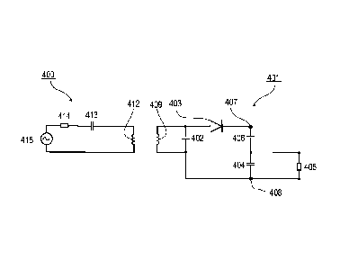
Reference is now made to Fig. 8, which illustrates an equivalent circuit
diagram for a
monitoring device according to a third embodiment of the invention. The
monitoring
device has a reader 400 and a data carrier 401. The reader 400 includes a
signal
generator 415, a resonance resistor 414, a resonance capacitor 413 and a
transmitter
coil 412. The resonance resistor 414, resonance capacitor 413 and transmitter
coil 412
together form a resonant circuit that is tuned to a resonance frequency that
corresponds
CA 02793377 2012-09-17
WO 2011/124251 PCT/EP2010/054534
8
to the chosen transmission frequency of the wireless signal from the reader
part. The
data carrier 401 includes a receiver coil 409, a resonance capacitor 402, a
rectifier 403,
an energy storage capacitor 404, a resistor 405 representing the load of the
monitoring
and data processing means on the data carrier, a modulation capacitor 406 and
connection points 407 and 408. The data carrier 401 is similar to the data
carriers
described with reference to Fig. 3 and Fig. 4.
The signal generator 415 generates an alternating current in the transmitter
coil 412.
The current in the transmitter coil generates an alternating magnetic field
which
induces an alternating current in the receiver coil 409. The frequency of the
alternating
magnetic field is denoted the operating frequency. The current in the receiver
is used to
power the data carrier.
According to an embodiment the data carrier is implanted in a human being for
continuous surveillance of a specific medical condition in the user. According
to a
further embodiment the data carrier has electrode means for recording EEG
signals of a
user and the data carrier is subcutaneously implanted in the user.
According to another embodiment the operating frequency is in the range
between 900
kHz and 1100 kHz, preferably about 1 MHz. Hereby is provided a monitoring
device
which can be made smaller than devices having a lower operating frequency
because
the requirements to the minimum size of the coils are relaxed when the
operating
frequency is increased. For a given design of the coil and with a given load
of the data
carrier, the Q factor of the resonance circuit on the data carrier will
generally increase
with the operating frequency. For a monitoring device according to various
embodiments of the invention this proportionality starts to diminish about 1
MHz due
to the skin effect.
It has been found that the resonance capacitor 202, 310 and 402 at an
operating
frequency of 1 MHz can have a capacitance in the range between 25 pF and 75
pF,
preferably about 50 pF, which is well above the parasitic capacitances. As
opposed to
this, a resonance capacitor with a capacitance in the range between 2 and 5 pF
is
required for an operating frequency of 10 MHz. Such small capacitance values
are
difficult to implement because they are too similar to the parasitic
capacitances.
CA 02793377 2015-11-06
52966-77
9
On the other hand it has been found that the power efficiency of the
monitoring device
can be increased with a factor of say 4 by increasing the operating frequency
from 100
kHz to 1 MHz in some embodiments.
Other modifications and variations of the structures and procedures will be
evident to
those skilled in the art.