Note: Descriptions are shown in the official language in which they were submitted.
CA 02793467 2012-10-19 111723 :911301 PCT
DESCRIPTION
TITLE OF INVENTION
Method of Manufacturing Silicon Carbide Semiconductor Device
TECHNICAL FIELD
The present invention relates to a method of manufacturing a silicon carbide
semiconductor device.
BACKGROUND ART
In manufacturing a semiconductor device, the step of selectively forming an
impurity region in a semiconductor substrate is performed. For example, in
manufacturing an n-channel type MOSFET (Metal Oxide Semiconductor Field Effect
Transistor), in order to obtain an npn structure, the step of partially
forming a p-type
impurity region in an n-type semiconductor substrate and further partially
forming an
n-type impurity region in this p-type impurity region is often performed.
Namely,
impurity regions different in extension from each other are formed. Both of
the
impurity regions should be formed in a self-aligned manner, in order to
suppress
variation in characteristics of the MOSFET, in particular. variation in
channel length.
In a case where a silicon substrate is employed as a semiconductor substrate,
a double
diffusion technique with which extension of an impurity region is adjusted by
adjusting
a degree of progress of impurity diffusion through heat treatment has widely
been used.
In a case where a silicon carbide substrate is employed as a semiconductor
substrate, however. a diffusion coefficient of an impurity is small and a
region into
which ions have been implanted becomes an impurity region substantially as it
is
through heat treatment. Therefore, it is difficult to employ the double
diffusion
technique. Thus, in order to obtain impurity regions formed in a self-aligned
manner,
a size of an opening in a mask for ion implantation should be adjusted. For
example,
according to Japanese Patent Laying-Open No. 2000-22137 (PTL 1), a
polycrystalline
silicon film or an oxide film formed by oxidizing the same is employed as a
mask and
different impurity regions are formed by making use of movement of a mask end
owing
-1-
CA 02793467 2012-10-19 111723 : 911301 PCT
to oxidation or oxide film removal.
CITATION LIST
PATENT LITERATURE
PTL 1: Japanese Patent Laying-Open No. 2000-22137
SUMMARY OF INVENTION
TECHNICAL PROBLEM
According to the technique described in the literature above, a sidewall of an
opening is subjected to thermal oxidation in order to narrow the opening in a
mask and
the oxide film is removed in order to widen the opening narrowed as such. A
thermal
oxidation step for adjusting the opening in the mask, however. may often be
undesirable or difficult. Specifically, a high temperature approximately from
900 to
1200 C required in the thermal oxidation step may give rise to a problem. For
example, in a case where a metal underlying layer is formed on a silicon
carbide
substrate, alloying may occur between a metal underlying film and the silicon
carbide
substrate at a high temperature. In addition.. a rate of oxidation in the
thermal
oxidation step is not much high, and for example, a rate of steam oxidation is
around 15
nm/minute. Therefore, efficiency in semiconductor device production may be
low.
Then, the following method is available as a method of narrowing an opening in
a mask. Initially, a film is formed on a silicon carbide substrate provided
with a mask
having an opening. As the film is formed on a sidewall of the opening, the
opening is
narrowed. Then, anisotropic etching allows a portion of the film on the
sidewall to
remain in the opening in the mask, while the remaining portion is removed. The
opening narrowed by the film can thus be obtained. With this method,. however,
anisotropic etching should be stopped at appropriate timing. If etching is
stopped too
early, a portion of the film to be removed remains and the remaining portion
may
interfere ion implantation. If etching is stopped too late, the film does not
sufficiently
remain on the sidewall and the opening may not sufficiently be narrowed.
Therefore,
simply by performing this method, it is difficult to accurately form an
impurity region.
The present invention was made in view of the problems above, and an object
CA 02793467 2012-10-19 111723:911301PCT
of the present invention is to provide a method of manufacturing a silicon
carbide
semiconductor device capable of forming impurity regions in an accurately self-
aligned
manner.
SOLUTION TO PROBLEM
A method of manufacturing a silicon carbide semiconductor device according to
the present invention has the following steps. A mask layer is formed on a
silicon
carbide substrate. The mask layer includes a cover portion covering the
silicon
carbide substrate and an opening having a sidewall. An impurity of a first
conductivity type is implanted onto the silicon carbide substrate through the
opening in
the mask layer. A first film made of a first material is formed on the silicon
carbide
substrate on which the mask layer has been formed. The first film includes a
first
portion arranged on the cover portion, a second portion arranged on the
sidewall of the
opening, and a third portion arranged on the silicon carbide substrate in the
opening.
A second film made of a second material different from the first material is
formed on
the silicon carbide substrate on which the mask laver and the first film have
been
formed. The second film includes a portion arranged on each of the first to
third
portions of the first film. Anisotropic etching for removing a portion of the
second
film arranged on the third portion of the first film is started. It is sensed
that etching
of the first material is performed during anisotropic etching. Anisotropic
etching is
stopped after it is sensed that etching of the first material is performed in
the step of
sensing that etching of the first material is performed. An impurity of a
second
conductivity type is implanted onto the silicon carbide substrate through the
opening
narrowed by the second portion of the first film and the second film arranged
on the
second portion after the step of stopping anisotropic etching.
According to the present invention, an end point of anisotropic etching of the
second film is detected by sensing that etching of the first film is
performed. Since
etching of the first film is performed not only in the opening in the mask
laver but also
on the cover portion of the mask layer, it can accurately be sensed that
etching of the
first film is performed. Therefore, since anisotropic etching of the second
film can
CA 02793467 2012-10-19 111723 :91 1301 PCT
accurately be stopped., the second film can accurately remain on the sidewall
of the
opening. Thus, since the impurity of the second conductivity type is implanted
through the accurately narrowed opening. a region of the second conductivity
type can
accurately be formed in a part of the region into which the impurity of the
first
conductivity type has been implanted through the opening.
In the manufacturing method above, the mask laver may be made of the second
material.
Since the material for the mask laver is thus the same as the material for the
second film, the method of manufacturing a silicon carbide semiconductor
device can
further be simplified.
In the manufacturing method above, after a first film is formed and before a
second film is formed, the following steps may be performed. A third film made
of a
material different from the first material is formed. A fourth film made of
the first
material is formed on the third film.
In this case, as etching proceeds, etching of the first material involved with
etching of the fourth film is sensed, and thereafter, at a time interval,
etching of the first
material involved with etching of the first film will be sensed. Namely, prior
to
sensing of etching of the first film, sensing predicting the same is carried
out.
Therefore. accuracy in stopping etching can further be enhanced.
In the manufacturing method above, an underlying layer may be formed on the
silicon carbide substrate before a mask laver is formed.
Thus, overetching of the silicon carbide substrate can be suppressed.
In the manufacturing method above, the underlying laver may be made of the
first material.
Thus. since the material for the underlying layer is the same as the material
for
the first film, the method of manufacturing a silicon carbide semiconductor
device can
further be simplified.
In the manufacturing method above, the underlying layer may be made of a
material different from the first material.
-4-
CA 02793467 2012-10-19 111723 : 911301PCT
Thus, a selective etching ratio between the underlying layer and the first
film
can be ensured, and hence accuracy in an amount of remaining underlying laver
after
anisotropic etching can be enhanced. Therefore, variation in implantation of
an
impurity of the second conductivity type through the underlying layer can be
suppressed.
In the manufacturing method above, the first material does not have to contain
a
metal element.
Thus, metal contamination of an apparatus for manufacturing a silicon carbide
semiconductor device can he avoided.
In the manufacturing method above, the first material may be made of any of a
silicon-based material and a carbon-based material.
Thus, the material for the first film can be free from a metal element.
ADVANTAGEOUS EFFECTS OF INVENTION
As is clear from the description above, according to the present invention,
impurity regions can be formed in an accurately self-aligned manner.
BRIEF DESCRIPTION OF DRAWINGS
Fig. 1 is a partial cross-sectional view schematically showing a construction
of a
silicon carbide semiconductor device in a first embodiment of the present
invention.
Fig. 2 is a partial cross-sectional view schematically showing a first step in
a
method of manufacturing a silicon carbide semiconductor device in Fig. 1.
Fig. 3 is a partial cross-sectional view schematically showing a second step
in
the method of manufacturing a silicon carbide semiconductor device in Fig. 1.
Fig. 4 is a partial cross-sectional view schematically showing a third step in
the
method of manufacturing a silicon carbide semiconductor device in Fig. 1.
Fig. 5 is a partial cross-sectional view schematically showing a fourth step
in
the method of manufacturing a silicon carbide semiconductor device in Fig. 1.
Fig. 6 is a partial cross-sectional view schematically showing a fifth step in
the
method of manufacturing a silicon carbide semiconductor device in Fig. 1.
Fig. 7 is a partial cross-sectional view schematically showing a sixth step in
the
-5-
CA 02793467 2012-10-19
111723:911301 PCT
method of manufacturing a silicon carbide semiconductor device in Fig. 1.
Fig. 8 is a partial cross-sectional view schematically showing a seventh step
in
the method of manufacturing a silicon carbide semiconductor device in Fig. 1.
Fig. 9 is a partial cross-sectional view schematically showing an eighth step
in
the method of manufacturing a silicon carbide semiconductor device in Fig. 1.
Fig. 10 is a partial cross-sectional view schematically showing a ninth step
in
the method of manufacturing a silicon carbide semiconductor device in Fig. 1.
Fig. 11 is a partial cross-sectional view schematically showing a tenth step
in
the method of manufacturing a silicon carbide semiconductor device in Fig. 1.
Fig. 12 is a partial cross-sectional view schematically showing an eleventh
step
in the method of manufacturing a silicon carbide semiconductor device in Fig.
1.
Fig. 13 is a partial cross-sectional view schematically showing a twelfth step
in
the method of manufacturing a silicon carbide semiconductor device in Fig. 1.
Fig. 14 is a partial cross-sectional view schematically showing a thirteenth
step
in the method of manufacturing a silicon carbide semiconductor device in Fig.
1.
Fig. 15 is a partial cross-sectional view schematically showing a fourteenth
step
in the method of manufacturing a silicon carbide semiconductor device in Fig.
1.
Fig. 16 is a partial cross-sectional view schematically showing a fifteenth
step
in the method of manufacturing a silicon carbide semiconductor device in Fig.
1.
Fig. 17 is a cross-sectional view schematically showing a first step in a
manufacturing method in a comparative example.
Fig. 18 is a cross-sectional view schematically showing a second step in the
manufacturing method in the comparative example.
Fig. 19 is a graph showing one example of how an end point is detected in the
comparative example.
Fig. 20 is a graph showing one example of how an end point is detected in the
first embodiment of the present invention.
Fig. 21 is a partial cross-sectional view schematically showing one step in a
method of manufacturing a silicon carbide semiconductor device in a second
-6-
CA 02793467 2012-10-19
111723:91 1301 PCT
embodiment of the present invention.
Fig. 22 is a graph showing one example of how an end point is detected in the
second embodiment of the present invention.
DESCRIPTION OF EMBODIMENTS
An embodiment of the present invention will be described hereinafter with
reference to the drawings.
(First Embodiment)
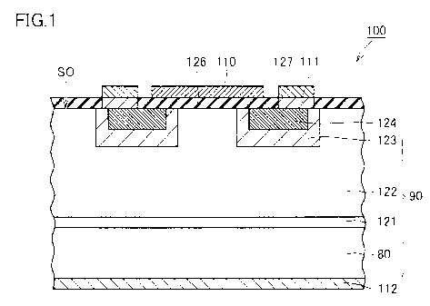
Initially, a structure of a MOSFET 100 representing a silicon carbide
semiconductor device in the present embodiment will be described with
reference to
Fig. 1. MOSFET 100 is specifically a vertical DiMOSFET (Double Implanted
MOSFET). MOSFET 100 has an epitaxial substrate 90, an oxide film 126, a source
electrode 111, an upper source electrode 127, a gate electrode 110. and a
drain
electrode 112. Epitaxial substrate 90 has a single crystal substrate 80, a
buffer layer
121, a breakdown voltage holding layer 122. a p region 123, and an n- region
124. A
two-dimensional shape (a shape when viewed from above in Fig. 1) of MOSFET 100
is.
for example, a rectangle or a square having a side of a length not shorter
than 2 mm.
Single crystal substrate 80 and buffer layer 121 each have an n conductivity
type. Single crystal substrate 80 is preferably composed of silicon carbide.
Concentration of an n-type conductive impurity in buffer laver 121 is, for
example.
5x10'7 cm-3. In addition, buffer laver 121 has a thickness, for example, of
0.5 m.
Breakdown voltage holding laver 122 is formed on buffer laver 121.. and it is
composed of silicon carbide having an n conductivity type. For example.
breakdown
voltage holding laver 122 has a thickness of 10 m and concentration of an n-
type
conductive impurity is 5x 101 cm 3.
In a surface SO of epitaxial substrate 90, a plurality of p regions 123 having
a p
conductivity type are formed at a distance from one another. In addition, in
surface
SO. n- region 124 is formed to be located inside each p region 123. In surface
SO, p
region 123 has a channel region lying between n- region 124 and breakdown
voltage
holding laver 122 and covered with gate electrode 110 with oxide film 126
being
-7-
CA 02793467 2012-10-19
111723 : 9 11301 PCT
interposed.
On breakdown voltage holding laver 122 exposed between the plurality of p
regions 123 at surface SO. oxide film 126 is formed. Specifically. oxide film
126 is
formed to extend from n region 124 in one p region 123 over p region 123.
breakdown
voltage holding layer 122 exposed between two p regions 123. and the other p
region
123 to n- region 124 in the other p region 123. Gate electrode 110 is formed
on oxide
film 126. Therefore, a portion of oxide film 126 having gate electrode 110
formed
thereon has a function as a gate insulating film. In addition. source
electrode 111 is
formed on n- region 124. A part of source electrode 11 l may be in contact
with p
region 123. Upper source electrode 127 is formed on source electrode 111.
A method of manufacturing MOSFET 100 will now be described below.
As shown in Fig. 2, epitaxial substrate 90 (silicon carbide substrate) having
surface SO is prepared. Specifically, buffer laver 121 is formed on a main
surface of
single crystal substrate 80, and breakdown voltage holding laver 122 is formed
on
buffer laver 121. Buffer layer 121 is composed of silicon carbide having an n
conductivity type, and it has a thickness, for example, of 0.5 urn. In
addition,
concentration of the conductive impurity in buffer layer 121 is set, for
example, to
5x10'7 cm-3 . Breakdown voltage holding laver 122 has a thickness. for
example. of
10 m. Further, concentration of the n conductive impurity in breakdown
voltage
holding layer 122 is set. for example, to 5x10¹⁵ CM 3.
As shown in Fig. 3, in the present embodiment. an etching stop laver 50 (an
underlying laver) is formed on surface SO of epitaxial substrate 90. A
material for
etching stop layer 50 is, for example. silicon nitride (SiN). titanium (Ti),
or silicon (Si).
Etching stop layer 50 has a thickness. for example. not smaller than 50 nm and
not
greater than 300 nm.
As shown in Fig. 4. a mask layer 31 is deposited on epitaxial substrate 90
with
etching stop layer 50 being interposed. Preferably, a material for mask laver
31 is any
of silicon oxide (SiO2) and polysilicon, and silicon oxide is more preferred.
As shown in Fig. 5. a photoresist pattern 40 is formed on mask laver 31 with
-8-
CA 02793467 2012-10-19
11172' : 911301 PCT
photolithography.
As shown in Fig. 6, mask laver 31 is patterned through anisotropic etching E1
using photoresist pattern 40 as a mask. Anisotropic etching E1 is specifically
dry
etching, and for example. it is reactive ion etching or ion milling. Then,
remaining
photoresist pattern 40 is removed.
As shown in Fig. 7. as a result of the steps so far, mask laver 31 having an
opening is formed on epitaxial substrate 90 with etching stop laver 50 being
interposed.
Specifically, mask layer 31 has a cover portion CV covering epitaxial
substrate 90 with
etching stop laver 50 being interposed and an opening OP having a sidewall S1.
In
terms of dimension specifications of MOSFET 1 00 (Fig. 1). in a plan view, an
area of
opening OP is normally smaller than an area of cover portion CV. Specifically,
a ratio
of the area of opening OP to the total area of cover portion CV and opening OP
(that is,
an area of mask layer 31) is preferably not higher than 5% and more preferably
not
higher than 3%, in terms of dimension specifications of MOSFET 100 (Fig. 1).
As shown in Fig. 8, as a result of ion implantation Jl through opening OP in
mask layer 31, a p-type (the first conductivity type) impurity is implanted
onto epitaxial
substrate 90. Thus. p region 123 is formed from surface SO to a prescribed
depth in
epitaxial substrate 90.
As shown in Fig. 9. thereafter. an end point film 32 (a first film) is formed
on
epitaxial substrate 90 on which etching stop layer 50 and mask laver 31 have
been
formed. End point film 32 has portions PI to P3. Portion PI (a first portion)
is
arranged on cover portion CV, portion P2 (a second portion) is arranged on
sidewall S I
of opening OP. and portion P3 (a third portion) is arranged on epitaxial
substrate 90 in
opening OP, with etching stop 'layer 50 being interposed. A material (a first
material)
for end point film 32 preferably does not substantially contain a metal
element. and it is,
for example, a silicon-based material or a carbon-based material. The silicon-
based
material is, for example, silicon nitride (SiN). The carbon-based material is.
for
example, carbon (C). In addition. a material for end point film 32 may be the
same as
a material for etching stop layer 50. In contrast, a material for end point
film 32 may
-9-
CA 02793467 2012-10-19
111723 : 911301PCT
be different from a material for etching stop laver 50.
As shown in Fig. 10. a spacer film 33 (a second film) is formed on epitaxial
substrate 90 on which mask laver 31 and end point film 32 have been formed.
Spacer
film 33 includes a portion arranged on each of portions P1 to P3 of end point
film 32.
Spacer film 33 is formed, for example, with p-CVD (plasma-Chemical Vapor
Deposition). In p-CVD, for example. a film formation temperature is around 400
C
and a rate of film formation is from 50 to 300 nm/minute.
Spacer film 33 is made of a material (a second material) different from the
material (the first material) for end point film 32. Preferably. a material
for each of
end point film 32 and spacer film 33 is selected such that atoms of at least
one type are
contained in only one of spacer film 33 and end point film 32. A material for
spacer
film 33 is. for example, silicon oxide (SiO2). Preferably. a material for
spacer film 33
is the same as a material for mask layer 31.
Then, anisotropic etching for removing a portion of spacer film 33 that is
arranged on portions P1 and P3 of end point film 32 is started. Anisotropic
etching is
dry etching, and for example. it is reactive ion etching or ion milling.
In addition, detection of an end point for identifying a type of a material
being
etched is started. An end point is detected. for example, based on
spectroscopic
analysis of light emitted during, etching or mass spectrometry of atoms
emitted by
etching.
As shown in Fig. 11, as anisotropic etching E2 proceeds, portions P1 and P3 of
end point film 32 are exposed. Accordingly, the material for end point film 32
starts
to be etched. Namely. etching of the material different from the material for
spacer
film 33 is started. Therefore, exposure of a part of end point film 32 is
sensed in end
point detection. In the present embodiment. etching by a prescribed amount is
further
performed after exposure of end point film 32 was sensed. In other words,
overetching is performed, so that portions P1 and P3 are removed. Thereafter,
anisotropic etching E2 is stopped. It is noted that this overetching may not
be
performed.
-10-
CA 02793467 2012-10-19
111723 :911301 PCT
As shown in Fig. 12. as a result of etching described above. a composite mask
30 having mask laver 31. end point film 32. and spacer film 33 is formed on
epitaxial
substrate 90 with etching stop laver 50 being interposed.
As shown in Fig. 13, as a result of ion implantation J2 through opening OP
narrowed by portion P2 of end point film 32 and spacer film 33 arranged on
portion P2.
an n-type (the second conductivity type) impurity is implanted onto epitaxial
substrate
90. Thus. n' region 124 is formed from surface SO to a prescribed depth in
epitaxial
substrate 90.
As further shown in Fig. 14. composite mask 30 and etching stop layer 50 are
removed. In addition, activation heat treatment is performed. This heat
treatment is
performed, for example, by performing heating at 1700 C in an argon atmosphere
for
30 minutes.
As shown in Fig. 15. oxide film 126 to serve as a gate insulating film is
formed
on epitaxial substrate 90. Specifically. oxide film 126 is formed to cover
breakdown
voltage holding layer 122. p region 123. and n region 124. Formation may be
carried
out by dry oxidation (thermal oxidation). Conditions in dry oxidation are, for
example,
a heating temperature of 1200 C and a heating time period of 30 minutes.
Thereafter. a nitriding heat treatment step is performed. This heat treatment
is
performed. for example.. by performing heating in a nitrogen monoxide (NO)
atmosphere at 1100 C for 120 minutes. Consequently. nitrogen atoms are
introduced
in the vicinity of an interface between each of breakdown voltage holding
layer 122. p
region 123 and n- region 124 and oxide film 126. It is noted that. after this
heat
treatment step using nitrogen monoxide. heat treatment using an argon (Ar) gas
which
is an inert gas may further be performed. Conditions in this heat treatment
are, for
example, a heating temperature of 1100 C and a heating time period of 60
minutes.
As shown in Fig. 16. source electrode 1 I 1 is formed. Specifically. the
following step is performed.
A resist film having a pattern is formed on oxide film 126 with
photolithography. Using this resist film as a mask, a portion of oxide film
126 located
-11-
CA 02793467 2012-10-19
111723: 911301 PCT
on n region 124 is etched away. Thus, an opening is formed in oxide film 126.
Then, a conductor film is formed in this opening to be in contact with n
region 124.
Then. by removing the resist film. a portion of the conductor film above that
has been
located on the resist film is removed (lift-off). This conductor film may be a
metal
film and it is composed, for example. of nickel (Ni). As a result of this lift-
off, source
electrode 111 is formed.
It is noted that heat treatment for alloying is preferably performed here. For
example, heat treatment for 2 minutes at a heating temperature of 950 C in an
atmosphere of an argon (Ar) gas which is an inert gas is performed.
Referring again to Fig. 1. upper source electrode 127 is formed on source
electrode 111. In addition. gate electrode 110 is formed on oxide film 126.
Moreover, drain electrode 112 is formed on a back surface (a lower surface in
the
drawing) of single crystal substrate 80. MOSFET 100 is obtained as described
above.
A comparative example will now be described. In the comparative example,
unlike the present embodiment (Fig. 10). spacer film 33 is formed without end
point
film 32 being provided (Fig. 17). It is assumed that mask layer 31 and the
spacer film
are made of silicon oxide and etching stop laver 50 is made of titanium.
Thereafter.
anisotropic etching as in the present embodiment is performed. As etching of
spacer
film 33 proceeds. an upper surface of mask layer 31 and etching stop laver 50
in
opening OP are exposed (Fig. 18). Here, since both of the material for spacer
film 33
and the material for mask layer 31 are silicon oxide, exposure of the upper
surface of
mask laver 31 cannot be an object to be detected as an end point. Therefore,
an object
to be detected as an end point is only exposure of etching stop layer 50 in
opening OP.
Variation in intensity I in end point detection (Fig. 19). that is. lowering
in 0 (oxygen)
atom intensity or increase in Ti (titanium) atom intensity, can theoretically
be detected.
Such variation in intensity, however., originates from difference in material
exposed
through opening OP. Therefore, as a ratio of an area of opening OP occupied in
mask
layer 31 is lower, variation in intensity is less. As thus variation in
intensity is less.
end point detection is actually difficult.
-12-
CA 02793467 2012-10-19
11 1723 :911301 PCT
In contrast, with end point film 32 (Fig. 10) being provided as in the present
embodiment. for example in a case where end point film 32 is made of silicon
nitride.
exposure of portion P 1 of end point film 32 at the upper surface of mask
laver 31 leads
to abrupt increase in nitrogen (N) atom intensity (Fig. 20). Therefore. since
end point
detection is easy, etching can accurately be stopped.
More generally discussing this aspect; according to the present embodiment. an
end point of anisotropic etching of spacer film 33 is detected based on
sensing of
etching of end point film 32 (Fig. 11) being performed. Since etching of end
point
film 32 is performed not only in opening OP (Fig. 9) in mask laver 31 but also
on cover
portion CV (Fig. 9) of mask laver 31. it can accurately be sensed that etching
of end
point film 32 is performed. As anisotropic etching of spacer film 33 can thus
accurately be stopped, spacer film 33 can accurately remain on sidewall S1 of
opening
OP. Therefore, since ion implantation J2 (Fig. 13) of the n-type impurity is
carried
out through accurately narrowed opening OP. an n-type region can accurately be
formed in a part of the region into which a p-type impurity has been implanted
(p
region 123) through opening OP.
In addition, as etching stop layer 50 is formed (Fig. 3). overetching of
epitaxial
substrate 90 can be suppressed (Figs. 11 and 12).
Preferably. the material for mask layer 31 is the same as the material for
spacer
film 33, and in this case. the method of manufacturing MOSFET 100 can further
be
simplified.
The material for etching stop layer 50 may be the same as the material for end
point film 32, and in this case, the method of manufacturing MOSFET 100 can
further
be simplified. Alternatively, they may be different from each other, and in
this case, a
selective etching ratio between etching stop laver 50 and end point film 32
can be
ensured. Therefore, accuracy in an amount of remaining etching stop laver 50
(Fig.
12) after anisotropic etching (Fig. 11) can be enhanced. Therefore, variation
in
implantation of an n-type impurity through etching stop laver 50 can be
suppressed.
Preferably, a material for end point film 32 does not contain a metal element,
so
-13-
CA 02793467 2012-10-19
111723:911301 PCT
that metal contamination of an apparatus for manufacturing MOSFET 100 can be
avoided.
(Second Embodiment)
In the present embodiment as well, initially, steps substantially similar to
those
in Figs. 2 to 9 (the first embodiment) are performed.
As shown in Fig. 21. then. an intermediate film 34 (a third film) made of a
material different from the material for end point film 32 is formed. An
intermediate
film 35 (a fourth film) made of a material the same as the material for end
point film 32
is formed on intermediate film 34. Spacer film 33 is formed on intermediate
film 35.
Preferably. a material for intermediate film 34 is the same as at least any of
a material
for mask layer 31 and a material for spacer film 33.
Then. MOSFET 100 (Fig. 1) is obtained through steps substantially similar to
those in Figs. 11 to 18 (the first embodiment).
Since a construction other than the above is substantially the same as the
construction in the first embodiment described above. the same or
corresponding
elements have the same reference characters allotted and description thereof
will not be
repeated.
According to the present embodiment, as etching proceeds, etching of a
material
for intermediate film 35 is sensed. and thereafter. at a time interval,
etching of the same
material involved with etching of end point film 32 will be sensed. Namely.
prior to
sensing of etching of end point film 32, etching of intermediate film 35,
which predicts
the same, is sensed. Therefore. accuracy in stopping etching can further be
enhanced.
For example. in a case where a material for each of mask layer 31,
intermediate film 34.
and spacer film 33 is silicon oxide, a material for each of end point film 32
and
intermediate film 35 is silicon nitride. and a material for etching stop layer
50 is
titanium, variation in intensity I as shown in Fig. 22 is sensed.
Specifically. prior to
final increase in N (nitrogen) atom intensity, peak of N atom intensity is
detected.
Though etching stop layer 50 is exposed at the time of ion implantation J2
(Fig.
13) in each embodiment above, this is not essential and end point film 32 may
remain
-14-
CA 02793467 2012-10-19
11172 3 : 911301 PCT
on etching stop laver 50. In addition. ion implantation J2 does not necessary
have to
be performed through etching stop laver 50 and etching stop laver 50 does not
have to
be formed.
In addition, though the p-type is defined as the first conductivity type and
the n-
type is defined as the second conductivity type, the n-type may be defined as
the first
conductivity type and the p-type may be defined as the second conductivity
type.
Preferably, a conductivity type is selected such that a semiconductor device
has an n-
type channel.
Further, though a MOSFET has been described in detail, a semiconductor
device may be a MISFET (Metal Insulator Semiconductor Field Effect Transistor)
other than the MOSFET. Furthermore, a semiconductor device may be other than a
MISFET and it may be. for example, an IGBT (Insulated Gate Bipolar
Transistor).
It should be understood that the embodiments disclosed herein are illustrative
and non-restrictive in every respect. The scope of the present invention is
defined by
the terms of the claims, rather than the description above, and is intended to
include any
modifications within the scope and meaning equivalent to the terms of the
claims.
REFERENCE SIGNS LIST
30 composite mask: 31 mask laver: 32 end point film (first film); 33 spacer
film
(second film); 34 intermediate film (third film): 35 intermediate film (fourth
film): 50
etching stop layer (underlying laver); 80 single crystal substrate; 90
epitaxial substrate
(silicon carbide substrate); CV cover portion; and OP opening.
-15-