Note: Descriptions are shown in the official language in which they were submitted.
CA 02793540 2014-08-26
Atty. Dkt. No.: 047711-5329
SENSOR SUBSTRATE SYSTEMS AND METHODS
100011
BACKGROUND
1. Field of the Invention
[0002] Embodiments of the present invention generally relate to sensor
technology, and.
in specific embodiments, to hermetically sealed substrates used for sensing a
variety of
io parameters, including physiological parameters.
2. Related Art
[0003] The combination of biosensors and microelectronics has resulted in the
availability
of portable diagnostic medical equipment that has improved the quality of life
for countless
people. Many people suffering from disease or disability who, in the past,
were forced to
15 make routine visits to a hospital or doctor's office for diagnostic
testing currently perform
diagnostic testing on themselves in the comfort of their own homes using
equipment with
accuracy to rival laboratory equipment.
[0004] Nonetheless, challenges in the biosensing field have remained. For
example.
although many diabetics currently utilize diagnostic medical equipment in the
comfort of
20 their own homes, the vast majority of such devices still require
diabetics to draw their own
blood and inject their own insulin. Drawing blood typically requires pricking
a finger. For
someone who is diagnosed with diabetes at an early age, the number of self-
induced finger
pricks over the course of a lifetime could easily reach into the tens of
thousands. In
addition, the number of insulin injections may also reach into tens of
thousands. Under any
25 circumstances, drawing blood and injecting insulin thousands of times is
invasive and
inconvenient at best and most likely painful and emotionally debilitating.
100051 Some medical conditions have been amenable to automated, implantable
sensing.
For example, thousands of people with heart conditions have had pacemakers or
defibrillators implanted into their bodies that utilize sensors for monitoring
the oxygen
30 content of their blood. Ideally, these sensors should be able to
determine whether, for
1
CA 02793540 2012-09-17
WO 2011/142903 PCT/US2011/031286
example, a person's heart is running very efficiently at a high heart rate or
whether a
person's heart has entered defibrillation. In order to make this determination
effectively, an
accurate sensor must be employed. Unfortunately, oxygen sensors implanted into
the body,
thus far, have typically required frequent and periodic checking and
recalibration. In fact,
one of the "holy grails" of the pacemaker industry has been an accurate, no
drift, no
calibration oxygen sensor. Until recently, such a sensor has been unavailable.
[0006] An ideal solution to the diagnostic requirements of those with disease
or disability,
absent an outright cure, is a sensor system that may be implanted into the
body and that may
remain in the body for extended periods of time without the need to reset or
recalibrate the
sensor. Regardless of the particular application for such a sensor system, in
order to affect
such a system the associated sensor must remain accurate, exhibit low drift
and require no
recalibration for extended periods. Such a system would typically require a
sensor to be
located in close proximity to sensing electronics in order to maintain the
required
characteristics.
[0007] However, attempts to place sensor electronics in close proximity to the
sensor in
implantable sensor systems have historically suffered from the environment in
which they
operate. For example, in an implantable sensor system for diabetics, a sensor
is needed to
detect an amount of glucose in the blood. Consequently, the sensor must be
implanted
within the body in such a manner that it comes into direct contact with the
blood. However,
in order to place the sensor electronics in such a system in close proximity
to the sensor, the
sensor electronics themselves must be placed into the blood as well. This
poses obvious
dangers for the sensor electronics. The sensor electronics must remain in
electrical contact
with the sensor; however, any exposure of the sensor electronics to the blood
or any other
fluid would potentially short circuit the sensor electronics and destroy the
entire system.
[0008] Thus, an ideal implantable sensor system would provide for a sensor to
be in close
proximity to sensor electronics while also providing hermeticity between the
sensor, which
may be exposed to fluids, and the sensor electronics, which must remain free
from short
circuiting fluids. In addition, the required hermeticity must be maintained
over the life of
the sensing system. The present invention provides such a system.
SUMMARY OF THE DISCLOSURE
[0009] A sensing apparatus may include a substrate having a first side for a
sensing
element and a second side for electronics. The substrate may have at least one
via from the
2
CA 02793540 2012-09-17
WO 2011/142903 PCT/US2011/031286
first side of the substrate to the second side of the substrate. The at least
one via may be
hermetically sealed from the first side of the substrate to the second side of
the substrate.
The at least one via may be at least partially filled with an optically
transmissive material.
[0010] In various embodiments, the optically transmissive material may
comprise a fritted
glass material. In some embodiments, the fritted glass material may comprise
at least one of
quartz and silica.
[0011] In various embodiments, the at least one via may be at least partially
filled with an
electrically conductive material. In some embodiments, the optically
transmissive material
may be concentrically arranged with respect to the electrically conductive
material. In some
embodiments, the electrically conductive material may comprise a fritless ink.
In some
embodiments, the electrically conductive material may comprise an indium tin
oxide.
[0012] In various embodiments, substrate may be made of a material comprising
ceramic.
In various embodiments, the at least one via may comprise a plurality of vias.
In some
embodiments, at least one of the plurality of vias may be at least partially
filled with an
optically transmissive material. At least one other of the plurality of vias
may be at least
partially filled with an electrically conductive material.
[0013] In various embodiments, the substrate may be annealed. In various
embodiments,
the at least one via may be filled with the optically transmissive material is
polished.
[0014] In various embodiments, the sensing apparatus may include the sensing
element.
The sensing element may be for sensing an analyte. In some embodiments, the
sensing
element may be for sensing a fluorescence resonance energy transfer of the
analyte. In
some embodiments, the sensing apparatus may include the electronics. The
electronics may
comprise an illumination device for illuminating the analyte.
[0015] In further embodiments, the illumination device may comprise at least
one of a
light emitting device, a vertical cavity surface emitting laser, and an edge
emitting laser. In
further embodiments, the illumination device may be arranged to illuminate the
analyte
through the at least one via in the substrate. In further embodiments, the
electronics may
include a sensor for measuring a returned fluorescence from the sensing
element. In yet
further embodiments, the sensor may be arranged to sense the returned
fluorescence from
the sensing element through the at least one via in the substrate.
[0016] A method of manufacturing a sensing apparatus may include, but is not
limited to,
any one of or combination of: (i) providing a substrate having a first side
for a sensing
element and a second side for electronics; (ii) forming at least one via from
the first side of
3
CA 02793540 2012-09-17
WO 2011/142903 PCT/US2011/031286
the substrate to the second side of the substrate; and (iii) filling the at
least one via at least
partially with an optically transmissive material such that the at least one
via is hermetically
sealed from the first side of the substrate to the second side of the
substrate.
[0017] In various embodiments, the method may include, but is not limited to,
any one of
or combination of: (iv) arranging at least one of optical emitting device and
a receiving
device on the second side of the substrate to pass light through the at least
one via to the
first side of the substrate; and (v) arranging an optically detectable
material that is reactive
in an optically detectable manner on the first side of the substrate to
receive light from the
optical emitting device and is optically detectable through the at least one
via by the
receiving device.
BRIEF DESCRIPTION OF THE DRAWINGS
[0018] FIG. 1 is a perspective view of a generalized substrate configuration
according to
an embodiment of the present invention.
[0019] FIG. 2A is a cut-away view of vias extending through a substrate
according to an
embodiment of the present invention.
[0020] FIG. 2B is a top view of a via arrangement on a substrate according to
an
embodiment of the present invention.
[0021] FIG. 3 is a flow diagram of a generalized process for fabricating a
sensor substrate
according to an embodiment of the present invention.
[0022] FIG. 4 is a flow diagram of a more detailed process for fabricating a
sensor
substrate according to an embodiment of the present invention.
[0023] FIG. 5 is a flow diagram of a process for filling vias with a filler
according to an
embodiment of the present invention.
[0024] FIG. 6A is a cut-away view of a filled via according to an embodiment
of the
present invention.
[0025] FIG. 6B is a cut-away view of a filled via and a filled meniscus
according to an
embodiment of the present invention.
[0026] FIG. 7 is a flow diagram for filling a meniscus according to an
embodiment of the
present invention.
[0027] FIG. 8 is a cut-away view of a hermetically filled via with excess
filler from a via
and a meniscus lapped off according to an embodiment of the present invention.
4
CA 02793540 2012-09-17
WO 2011/142903 PCT/US2011/031286
[0028] FIG. 9 is a flow diagram of a process for preparing one side of a
substrate to accept
an IC and another side to accept a sensing element according an embodiment of
the present
invention.
[0029] FIG. 10A is a perspective view of a substrate with aluminum pillars
formed on top
of vias according to an embodiment of the present invention.
[0030] FIG. 10B is a perspective view of a substrate with aluminum pillars
formed on top
of vias coated with an alumina coating according to an embodiment of the
present
invention.
[0031] FIG. 10C is a perspective view of a substrate with pillars removed
according to an
embodiment of the present invention;
[0032] FIG. 11 is a perspective view of a photoresist corresponding to an
electrode pattern
according to an embodiment of the invention.
[0033] FIG. 12 is a flow diagram of a process for affixing an IC to an
electronics side of a
substrate according to an embodiment of the present invention.
[0034] FIG. 13 is a flow diagram of a process for forming a lid according to
an
embodiment of the present invention.
[0035] FIG. 14 is a flow diagram of a process for performing a gross leak test
according to
an embodiment of the present invention.
[0036] FIG. 15 is a flow diagram of a process for electroplating and coating
the substrate
according to an embodiment of the present invention.
[0037] FIG. 16 is a perspective view of a finally assembled sensor substrate
according to
an embodiment of the invention.
[0038] FIG. 17 is a flow diagram of a generalized process for fabricating a
sensor
substrate according to an embodiment of the present invention.
[0039] FIG. 18 is a flow diagram of a generalized process for fabricating a
sensor
substrate according to an embodiment of the present invention.
[0040] FIGS. 19A-19D show filled vias according to various embodiments of the
present
invention.
[0041] FIG. 20 is a cut-away view of a substrate with a filled via and
associated
electronics according to an embodiment of the present invention.
[0042] FIG. 21 is a cut-away view of a substrate with a filled via and
associated
electronics according to an embodiment of the present invention.
5
CA 02793540 2014-08-26
Atty. Dkt. No.: 047711-5329
DETAILED DESCRIPTION
[0043] FIG. 1 shows a generalized substrate configuration according to an
embodiment of
the present invention. In various embodiments. the substrate as discussed
throughout the
disclosure may be employed in a sensor system as will be discussed in detail.
In other
embodiments, the substrate may be employed in catheters, subcutaneous
implants, vascular
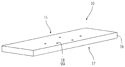
implants, external sensors, and/or the like. A sensor 10 may have a sensing
element side 12
of a substrate 16 on which a biosensing element, physiological parameter
sensing element
or other sensing element may be affixed. The sensor 10 may have an electronics
side 14 of
the substrate 16 on which electronics may be affixed for processing signals
generated by the
io seiisiiig element. The sensor 10 (and/or components thereof) and/or the
processes for
producing such a sensor (and/or components thereof) are discussed throughout
this
disclosure.
[0044] Other examples of the sensor 10 (and/or components thereof) and/or the
processes
for producing such a sensor (and/or components thereof) may be found in the
following
U.S. Patent Applications that were assigned to the assignee of the present
invention:
(i)
U.S. Patent Application Serial No. 10/331,186, filed December 26, 2002; (ii)
U.S. Patent
Application Serial No. 10/671,996, filed September 26, 2003; (iii) U.S. Patent
Application
Serial No. 10/845,002, filed May 12, 2004; (iv) U.S. Patent Application Serial
No.
11/086,936,186, filed March 22, 2005; (v) U.S. Patent Application Serial No.
11/868,898,
filed October 8, 2007; (vi) U.S. Patent Application Serial No. 12/271,134,
filed November
14, 2008; (vii) U.S. Patent Application Serial No. 10/038,276, filed January
2, 2002: (viii)
U.S. Patent Application Serial No. 10/861,976, filed June 4, 2004; (ix) U.S.
Patent
Application Serial No. 10/996,026, filed November 22, 2004; (x) U.S. Patent
Application
Serial No. 11/924,402, filed October 25, 2007; (xi) U.S. Patent Provisional
Application
Serial No. 60/414,289, filed September 27, 2002; and (xii) U.S. Patent
Provisional
Application Serial No. 60/318,055, filed September 7, 2001.
[0045] The sensing element side 12 may support any of a variety of sensing
elements. For
example, the sensing element may be a glucose sensor utilizing a glucose
oxidase enzyme
as a catalyst. Alternatively, the sensing element may be an oxygen sensor or
may include a
plurality of sensing elements. In various embodiments, the sensing element may
be a sensor
for sensing cholesterol, glutamate, alcohol, lactate, or any other molecules
that have an
6
CA 02793540 2012-09-17
WO 2011/142903 PCT/US2011/031286
oxidase-based enzyme. In various embodiments, the sensing element may be a
sensor for
sensing a redox reaction and/or the like.
[0046] The electronics side 14 may support a variety of electronic circuits.
According to
one embodiment of the invention, the electronics side 14 of the substrate 16
may support an
application specific integrated circuit (ASIC) containing data acquisition
circuitry. Thus,
analog signals received from the sensing element on the sensing element side
12 of the
substrate 16 may be digitized by the ASIC on the electronics side 14 of the
substrate 16. By
positioning digitizing and other electronics close to the source of the analog
signals and
avoiding long cables along which signals are typically sent to be digitized,
noise levels,
offsets, and signal loss may be reduced. As a result, accuracy and reliability
of the device
may be increased. In addition, once the signals have been digitized by the
electronics on the
electronics side 14 of the substrate 16, the digitized signals may be sent to
other devices for
operation or other processing in discrete form rather than analog form, which
may result in
improved leakage, drift, and other characteristics.
[0047] One or more vias 18 may extend from the sensing element side 12 of the
substrate
16 to the electronics side 14 of the substrate 16. As shown in FIG. 2A, the
vias 18 are
pathways through the body of the substrate 16 that allow for communication
(e.g., electrical
contact) between an array of electrodes or other electrical contacts reacting
with the sensing
element on the sensing element side 12 of the substrate 16 and electronics on
the electronics
side 14 of the substrate 16.
[0048] The vias 18 may be arranged in a variety of fashions. A via arrangement
for one
sensing element according to one embodiment of the present invention may be
seen in FIG.
2B. The via arrangement shown in FIG. 2B may correspond to electrodes that
interact with
an enzyme used as a catalyst in the sensing element. A first via 18a and a
second via 18b
may correspond to a first working electrode and a first counter electrode. A
third via 18c
and a fourth via 18d may correspond to a second working electrode and a second
counter
electrode. A fifth via 18e may correspond to a reference electrode. Electrodes
may be
arranged to line up with the vias 18, for example, using one of the processes
described
throughout this disclosure.
[0049] In various embodiments, the generalized substrate configuration of
electronics
adjacent to a sensing element on opposite sides of the substrate 16 (FIG. 1)
and the resulting
ability to output discrete signals rather than analog signals from the sensor
results in a stable
device. Sensor electrode output drift of less than 5% over periods of one year
or more may
7
CA 02793540 2012-09-17
WO 2011/142903 PCT/US2011/031286
be possible using such embodiments. With such a low drift specification,
replacement or
calibration intervals may be greatly reduced, allowing such embodiments to be
implanted
into a human body for extended periods.
[0050] The generalized substrate configuration shown in FIG. 1 benefits from
processes
according to embodiments of the present invention, to be described below, that
result in
hermeticity between the sensing element side 12 of the substrate 16 and the
electronics side
14 of the substrate 16. In various embodiments, hermeticities corresponding to
a helium
leak rate of 1 x 10⁻⁸ cc/sec at 1 atmosphere over a three-year period may be
obtained.
[0051] In addition, in various embodiments, the sensor 10 may be implanted
into the
human body, for example, residing in a vein or artery. In addition, the
sensing element side
12 of the substrate 16 may be exposed to fluids, such as, for example, blood.
In this type of
use, should the fluids infiltrate the electronics on the electronics side 14
of the substrate 16,
the fluids would destroy the electronics and render the device useless.
However, because
the electronics side 14 of the substrate 16 may be hermetically sealed from
the sensing
element side 12 of the substrate as discussed throughout this disclosure,
electronics may be
placed directly on the electronics side 14 of the substrate 16 without
exposure to fluids or
other elements encountered by the sensing element that may damage the
electronics.
[0052] The substrate 16 may be fabricated from a variety of materials.
According to one
embodiment of the present invention, the substrate 16 may be fabricated from
ceramic. For
example, the substrate 16 may be fabricated using a pressed ceramic slurry in
tape form,
which is widely available commercially. Also according to one embodiment of
the
invention, a substrate of 92%-96% alumina (A1203) may be used. The substrate
material
may be bought in sheet form, which may be flexible or rigid.
[0053] The substrate 16 may take a variety of forms and may be structured in a
variety of
ways in addition to the configuration shown in FIG. 1. For example, according
to one
embodiment of the invention the substrate 16 may have more than two sides on
which one
or more sensing elements or electronics may be placed. The substrate 16 may be
a multi-
surface device with sensing elements and electronics on any of multiple
surfaces and having
multiple vias extending in a variety of geometries to affect electrical
contact between
surfaces.
[0054] In another embodiment of the invention, one or more sensing elements
and
electronics may be on the same side of the substrate 16. The vias 18 may be
arranged
accordingly to effect electrical contact between one or more sensing elements
and
8
CA 02793540 2012-09-17
WO 2011/142903 PCT/US2011/031286
electronics, irrespective of the position of a sensing element and electronics
on the substrate
16.
[0055] FIG. 3 shows a generalized process for fabricating a sensor substrate
according to
an embodiment of the present invention. Although the process detailed in FIG.
3 refers to a
substrate, it is to be understood that the process may be applied to a
plurality of substrates
formed from a single board of substrate material. With reference to FIGS. 1-3,
substrate
material may be obtained at step 20. At step 22, vias 18 may be formed in the
substrate 16
such that a hollow path is created from one side of the substrate 16 to
another. The vias
may be laser drilled, punched, or formed in other manner common in the
industry.
[0056] At step 24, the vias 18 may be filled with a material that is
electrically conductive
such that electrical continuity exists between one side of the substrate 16
and another. In
addition, the vias 18 may be filled such that a hermetic seal exists between
one side of the
substrate 16 and another. At step 26, conductive layers may be deposited onto
each side of
the substrate 16 that make electrical contact with the vias 18. At step 28,
electronics may be
placed on one side of the substrate 16 and a sensing element may be placed on
another side
of the substrate 16, both being placed in such a manner that they make the
desired contact
with the conductive layers.
[0057] FIG. 4 shows a more detailed process for fabricating a sensor substrate
according
to an embodiment of the present invention. Although the process detailed in
FIG. 4 refers
to a substrate, it is to be understood that the process may be applied to a
plurality of
substrates formed from a single board of substrate material.
[0058] A variety of fabrication techniques may be used during the fabrication
of the
sensor substrate. For example, either thin film or thick film fabrication
technologies may be
used. The generalized process shown in FIG. 4 (or any other process described
in the
disclosure) is for purposes of illustration only, and should not limit
embodiments of the
invention in any way.
[0059] With reference to FIGS. 1, 2A, 2B, and 4, substrate material may be
obtained at
step 30. As stated previously, according to a typical embodiment of the
present invention, a
92%-96% alumina substrate (A1203) may be used. Alumina is widely used in the
microelectronics industry and is available from many resources. For example, a
96%
alumina substrate may be purchased from (but is not limited to) COORS, INC.
[0060] Although 99.6% alumina is typical in electrode based sensor
applications because
of its purity, which typically results in enhanced device resistance, 92%-96%
alumina may
9
CA 02793540 2012-09-17
WO 2011/142903 PCT/US2011/031286
be used in various embodiments for enhanced performance during annealing and
testing
processes of embodiments of the present invention. On a substrate of greater
than 96%,
alumina cracks resulting from laser drilling of the vias may not anneal as
well as 92%-96%
alumina.
[0061] A substrate of less than 92% alumina typically has a surface with
increased
roughness and granularity, which may make it difficult to print on and seal.
In addition,
testing of a substrate of less than 92% alumina may be difficult because the
substrate
surface may absorb helium used during leak detection and may be more
susceptible to
corrosion. Moreover, a substrate of less than 92% alumina is typically darker
than 92%-
96% alumina and may affect photolithography processes used in embodiments of
the
present invention.
[0062] At step 32, vias 18 may be formed in the substrate 16 such that a
hollow path is
created from one side of the substrate 16 to another. The vias 18 may be laser
drilled,
punched, or formed in other manner common in the industry.
[0063] At step 34, the substrate 16 may be annealed. If the process used for
forming vias
18 results in cracks on the surface of or within the body of the substrate 16,
annealing of the
substrate 16 may be performed to mend such cracks. According to one embodiment
of the
present invention, the substrate 16 may be annealed at approximately 1200 C
for
approximately 16 hours. If the process used for forming vias 18 does not
result in cracks on
the surface of or within the body of the substrate 16 and hermeticity from one
side of the
substrate 16 to another is possible without annealing, the annealing step may
be avoided.
[0064] The vias 18 may be filled at step 36. The vias 18 may be filled with
any
electrically conductive material that can be packed densely enough to provide
hermeticity
from one side of the substrate 16 to another. The filler should be
electrically conductive so
that an electrically conductive path is formed from one side of the substrate
16 to another,
allowing electrical contact between components on each side of the substrate
16, such as,
for example, sensor electrodes on one side of the substrate 16 and electronic
circuitry on
another side.
[0065] According to one embodiment of the present invention, the vias 18 may
be filled
with an electrically conductive filler. For example, the vias 18 may be filled
with a fritted
or fritless ink, such as, but not limited to, a gold or a platinum paste,
and/or the like. Fritless
ink is generally more desirable than fritted ink in this application because
fritted ink
typically comprises too many fillers and particulates to facilitate the
formation of a densely
CA 02793540 2012-09-17
WO 2011/142903 PCT/US2011/031286
packed via. In various embodiments, in order to provide hermeticity from one
side of the
substrate 16 to another, the filling of the via 18 must be such that voids or
gaps that would
support the development of moisture do not exist within the material used to
fill the via 18.
[0066] According to one embodiment of the present invention, a 96% alumina
substrate,
which may be purchased off the shelf from a variety of manufacturers, such as
COORS,
INC., may be filled with a gold paste. If another type of substrate is used,
such as, for
example, a 92% alumina substrate, which may be custom, made, the substrate may
be
purchased with the vias already filled with a filler, such as for example,
platinum paste.
[0067] A process of filling vias with a filler according to an embodiment of
the present
invention is shown in FIG. 5. With reference to FIGS. 1, 2A, 2B, 4, and 5, at
step 42, a
screen with a via pattern may be placed on top of the surface of the
substrate. A stencil may
also be used. At step 44, a filler, such as fritless ink, may be pushed
through the screen into
the via 18 in a "squeegee" fashion. At step 46, a vacuum may be pulled on a
side of the
substrate 16 opposite the side on which the filler has been pushed into the
via 18 such that
the filler coats the walls of the via 18. Filling vias in a vacuum may
facilitate intimate
contact with surfaces and dense packing.
[0068] After the filler has coated the walls of the via 18 in step 46, the
substrate 16 may
be fired in step 48 so that the filler is hardened, i.e., it becomes solid. At
step 50, the via 18
may be checked to determine whether the via 18 is completely plugged. If the
via 18 is
completely plugged, the process of filling the via 18 according to an
embodiment of the
present invention is complete. If the via 18 is not completely plugged, steps
42-48 may be
repeated as many times as is necessary until the via 18 is completely plugged
with the filler.
[0069] A via 18 filled according to the process of FIG. 5 may be seen in FIG.
6A. A
substrate 16 containing a via 18 has been filled with a filler 60. Successive
applications of
the filler 60 results in layers of the filler 60 extending throughout the
hollow area of the via
18 until the filler 60 plugs the via 18 and eliminates any pathway from one
side of the
substrate 16 to another. A meniscus 62 typically forms on either side of the
via 18 after the
via 18 has been filled with the filler 60.
[0070] With reference to FIGS. 4 and 6A, the meniscus 62 that typically forms
during the
filling of the vias 18 may be filled at step 38. The meniscus 62 may be filled
with the same
filler 60 that was used to plug the vias 18.
[0071] FIG. 7 shows a process for filling the meniscus 62 according to an
embodiment of
the invention. With reference to FIGS. 4, 6A, and 7, at step 70, the substrate
16 may be put
11
CA 02793540 2014-08-26
Atty. Dkt. No.: 047711-5329
into (or otherwise exposed to) a vacuum. At step 72, a filler 60 may be
printed onto the top
of the meniscus 62. The printing process used may be the same process detailed
earlier
(e.g.. FIG. 5) for filling the vias 18 or may be another suitable process. At
step 74, the
substrate 16 may be then vented to atmosphere. Venting the substrate 16 to the
atmosphere
introduces an atmospheric pressure on the filler 60, which may push down on
the Filler 60 ill
the meniscus 62 and displaces any gap that might be in the meniscus 62 or via
18.
100721 At step 76, the substrate 16 may be fired such that the filler 60 in
the meniscus 62
is hardened. Firing of the substrate also burns off any organics, solvents, or
other
impurities. According to one embodiment of the present invention, if the
filler 60 used is a
-up fritless ink such as, for example, gold or platinum paste. the
substrate 16 may be First Fired
at 300-400 C to burn off organics, solvents, or other impurities. The
substrate 16
subsequently may be fired at 900-1000 C. At 900-1000 C, the filler 60 may
sinter. The
firing time may typically be a few hours for every firing cycle. After firing
the filler 60 to
sinter the filler 60, the substrate 16 may be cooled such that the filler 60
hardens. In some
embodiments, cooling must be done at a rate slow enough such that the
substrate 16 does
not crack, which would compromise the hermeticity of the device. Steps 70-76
may be
repeated as often as necessary to fill the meniscus 62 and the layers of
filler 60 that extend
above the substrate. A substrate 16 with a filled via 18 and a filled meniscus
62 may be
seen in FIG. 6B.
[0073] With reference to FIGS. 4, 6A, and 6B, at step 40 the excess filler 60
that extends
above the surface of the substrate 16 resulting from the filling of the vias
18 and the
meniscus 62 may be lapped off so that the filler 60 is even with the surface
of the substrate
16. The filler 60 may be lapped off using tools and techniques common in the
industry,' so
long as the hermetic integrity of the substrate 16 is not compromised. A
substrate 16 with
excess filler 60 lapped off and hermetically sealed vias 18 may be seen in
FIG. 8.
[0074] Thus, subsequent to step 40 in FIG. 4, a process according to
embodiments of the
present invention has generated a substrate 16 that is hermetically sealed
from one side to
another. With reference to FIGS. 1-8, it should be understood at this point
that the
fabrication of the substrate 16 for hermetic ity is not limited to the process
described (e.g.,
FIG. 4). Other steps or processes may be introduced, or steps may be
eliminated.
For example,
depending on the type of filler 60 used to fill the vias 18 and the meniscus
62, the annealing
steps and the firing steps may be performed at the same time. Other variations
in the
12
CA 02793540 2012-09-17
WO 2011/142903 PCT/US2011/031286
process are also possible while still maintaining the essence of embodiments
of the present
invention.
[0075] The substrate 16 with hermetically sealed vias 18 may be used for a
variety of
applications. According to embodiments of the present invention, the substrate
16 may now
be prepared to accept a sensing element on one side of the substrate and
electronics on
another side of the substrate 16. As before, the substrate 16 may be prepared
using a variety
of techniques, including (but not limited to), for example, thin film or thick
film deposition
processes. For purposes of illustration, and not by way of limitation,
processes according to
embodiments of the present invention will be described below using thin film
deposition
techniques.
[0076] Electronics may be affixed to one side of the substrate 16 and may take
a variety of
forms. For example, the electronics may take the form of an integrated circuit
(IC), such as,
for example, an ASIC, a microcontroller, or a microprocessor. Alternatively,
the electronics
may take the form of discrete components.
[0077] In addition, a sensing element may be affixed to another side of the
substrate 16.
FIG. 9 shows a process according to embodiments of the present invention for
preparing
one side of the substrate 16 (e.g., FIG. 8) to accept an IC and another side
to accept a
sensing element.
[0078] With reference to FIGS. 1-9, at step 80, a side of the substrate 16
being prepared
for an IC may have a metallization pattern applied to it using standard resist
photolithography or other techniques common in the industry. This layer of
metallization is
the conductor that provides continuity from the portion of a via 18 on the
sensing element
side of the substrate 16 to a bonding pad on an IC side of the substrate 16.
In practice, this
layer may actually be two, three, or more layers. For example, the
metallization layer may
be a titanium-platinum layer or the like. Alternatively, the metallization
layer may be a
titanium-platinum-titanium layer or the like. The pattern may correspond to
the pins of the
IC or may be some other pattern depending on the desired application.
[0079] At step 82, aluminum pillars 100 may be placed on top of the vias 18. A
ceramic
or other material mask (not shown) may be laser drilled, punched or otherwise
worked to
form openings corresponding to the via pattern on the substrate. According to
one
embodiment of the present invention, the openings may be 20-25 microns deep.
The mask
then may be affixed to the substrate 16 on top of the metallization pattern
applied during
step 80. Then aluminum may be deposited through the openings to form pillars
20-25
13
CA 02793540 2012-09-17
WO 2011/142903 PCT/US2011/031286
microns high. Once the aluminum pillars 100 have been formed, the mask may be
removed, leaving the 20-25 micron aluminum pillars 100 on top of the vias 18.
A substrate
16 with aluminum pillars 100 formed on top of the vias 18 according to an
embodiment of
the present invention may be seen in FIG. 10A.
[0080] With reference to FIGS. 9 and 10A, after step 82, the entire substrate
16 may be
coated with an alumina coating at step 84. According to one embodiment of the
present
invention, the entire substrate 16 may be put into a vacuum chamber and
blanket coated
with an alumina coating. A variety of processes may be used to blanket coat
the substrate
16 with alumina. For example, chemical vapor deposition (CVD), epitaxial
deposition,
sputtering, or evaporation may be used to blanket coat the substrate 16 with
the alumina
coating. Alternatively, ion beam assist deposition (IBAD) may be used. IBAD is
a
combination of two distinct operations: physical vapor deposition combined
with
bombarding the surface of the substrate 16 with low energy ions. Bombarding
the surface
of the substrate 16 with low energy ions may allow for better adhesion and
higher density of
the alumina coating.
[0081] Using an IBAD process to coat the substrate 16 with alumina may provide
pin-hole
free layers of alumina, which enhances the overall hermeticity of the device.
In other
words, coating the substrate 16 with alumina using the IBAD process may
prevent the
transmission of vapor, moisture, fluids, or other elements that would
compromise the
hermetic integrity of the device.
[0082] According to one embodiment of the invention, the alumina coating may
be 12
microns deep. Consequently, at the end of step 84, the substrate 16 will have
aluminum
pillars 100 rising 8-13 microns above a 12 micron alumina sheet. A
configuration
according to this embodiment of the present invention may be seen in FIG. 10B.
[0083] With reference to FIGS. 9 and 10B, at step 86, the entire substrate 16,
including
the alumina coating and the aluminum pillars 100, may be put into a dissolving
solution
such as, for example, ferric chloride (FeC13) or other solution strong enough
to dissolve the
aluminum pillars 100 but mild enough not to attack the alumina coating. Thus,
after the
aluminum pillars 100 dissolve, the substrate 16 will be covered with an
alumina coating 12
microns high with recesses permitting access to the vias. This configuration
may be seen in
FIG. 10C.
[0084] With reference to FIGS. 9 and 10C, at step 88, the metallization layer
supporting
the IC and any other components being affixed to the electronics side 14 of
the substrate 16
14
CA 02793540 2012-09-17
WO 2011/142903 PCT/US2011/031286
may be applied. Any suitable metal may be applied using any suitable process.
For
example, a metallization using gold (or the like) may be applied with a thin
film process.
The pattern may take a variety of shapes. For example, according to one
embodiment of the
invention, the pattern may resemble a "ring" or a "racetrack."
[0085] In addition, the gold may fill the recesses created by the aluminum
pillars 100 that
were previously dissolved. In various embodiments, hermeticity will generally
not be
required at this layer since the substrate has already been hermetically
sealed by this point in
the process of such embodiments. Accordingly, the metallization layer may be
6000 to
10000 angstroms. Once this layer of metallization has been applied, the IC,
and any other
components, such as, for example, capacitors, may be wired bonded or otherwise
connected
to the pads. Additionally, any other component, such as a lid for the
electronics, for
example, may be affixed to the electronics side of the substrate subsequent to
step 88.
[0086] At step 90, a side of the substrate 16 being prepared for a sensing
element may be
provided with a metallization pattern. A variety of techniques may be used to
apply the
metallization pattern to the side of the substrate being prepared for a
sensing element. For
example, a metallization pattern may be applied to the substrate 16 by etching
the
metallization pattern onto the substrate 16. Alternatively, a metallization
pattern may be
applied to the substrate 16 using common photoresist techniques.
[0087] According to one embodiment of the invention, if common photoresist
techniques
are used, a photoresist may first be applied to the substrate. The photoresist
may be a
positive resist, which becomes soluble when interacting with light, or a
negative resist,
which becomes insoluble when interacting with light. If a positive resist is
used, a mask
may be put over the photoresist and then the mask and the photoresist may be
exposed to
light. Thus, light going through openings on the mask solubilizes the unmasked
portions of
the photoresist. Then, the mask may be washed off, and, consequently, the
substrate will
have a cured coating of photoresist where the unmasked photoresist was exposed
to light. A
photoresist corresponding to an electrode pattern according to one embodiment
of the
invention may be seen in FIG. 11. The electrodes may have tie bars or the like
to provide a
conductive path for electroplating. The working and counter electrodes may be
metallized.
[0088] Next, the cured photoresist may be metallized using a variety of
techniques. Any
thin film deposition technique may be used, such as, for example, sputtering.
Thus,
according to one embodiment of the invention, the substrate may be put into a
vacuum,
then, sputtered with a first metal, such as, for example, titanium, and then
sputtered with a
CA 02793540 2012-09-17
WO 2011/142903 PCT/US2011/031286
second metal, such as, for example, platinum. Accordingly, a conductive layer
may be
placed between the vias and alumina caps in order to maintain electrical
conductivity.
[0089] Next, the photoresist may be washed away. For example, the photoresist
may be
put into an acetone ultrasonic bath or the like. Thus, a photoresist not cured
during
exposure to light by the mask will dissolve and metal deposited on the uncured
photoresist
will be washed away.
[0090] With reference to FIGS. 9-11, at step 92, caps may be placed over the
via
locations. Oxygen reduction may occur at the working electrodes and create
hydroxyl ions,
thus creating an alkaline local environment. As the device operates, the
hydroxyl ions may
attack the electrode/via interface. The electrode/via interface initially may
be hermetic, but
can be broken down if the hydroxyl ions interact with the via 18 for an
extended period.
Thus, to extend life of the via 18 a cap (not shown) may be placed over the
via 18 to keep
current from the electrochemical process of the hydroxyl ions from entering
the via 18, thus
extending life of the via 18 and improving reliability of the via 18. In other
words, caps
may be used to prevent byproducts of detection electrochemistry from
compromising via
hermeticity by preventing corrosive attack of both the via 18 and the annealed
surfaces of a
laser drilled opening.
[0091] A variety of techniques may be used to place a cap over the vias 18.
For example,
alumina caps may be deposited over the via 18 using an IBAD process. A shadow
mask
may be used during the process similar to the technique used to apply the
aluminum pillars
100. Caps may be formed with a positive shadow mask, which may be used where
alumina
deposited through an aperture remains in place on a finished substrate. The
cap position
may be adjusted (e.g., a length of the cap may be adjusted along the
electrode) changing the
configuration of the active electrodes to the windows. The sensitivity of the
sensor can
depend on the cap position, or the resulting position of the active electrode
to the window.
[0092] As an alternative to placing caps over vias 18, caps may be placed over
electrodes
to inhibit oxygen reduction at the electrodes. According to embodiments of the
invention,
caps placed over the vias 18 or the electrodes may be about 18 microns in
thickness.
[0093] Once an electronics side 14 (FIG. 1) of the substrate 16 and a sensing
element side
12 (FIG. 1)of the substrate 16 has been prepared to accept electronics and a
sensing
element, respectively, electronics and a sensing element may be affixed to the
substrate. A
process for affixing an IC to the electronics side of the substrate 16 may be
shown in FIG.
12.
16
CA 02793540 2012-09-17
WO 2011/142903 PCT/US2011/031286
[0094] With reference to FIGS. 1 and 12, at step 110, an IC may be epoxied or
otherwise
adhered to a rectangular pad in the center of the substrate 16. At step 111,
leads of the IC
may be wired bonded to the gold pads earlier formed on the electronics side 14
of the
substrate 16.
[0095] According to some embodiments of the invention, a capacitor may be used
in
connection with the IC. The capacitor may serve as a power supply instead of a
battery and
may be large enough to maintain a DC voltage in between pulses. If a capacitor
is used, at
step 112 a solder paste may be placed on the capacitor and the capacitor may
be put into
position on the substrate 16.
[0096] At step 113, a layer of solder paste may be placed along the entire
gold ring
previously deposited on the electronics side 14 of the substrate 16. At step
114, the entire
substrate 16 may be reflowed at temperature, including the solder paste
deposited on the
gold ring. The entire substrate 16 may then be put through cleaning cycles at
step 115 to
remove residual material, such as flux residue from solder paste.
[0097] According to one embodiment of the invention, a lid may be placed over
the
electronics. At step 116, the lid may be held by a fixture over the substrate
16 and the
substrate 16 may be baked to remove moisture. For example, the substrate 16
may be baked
at 150 C for 12 hours at less than 1 torr to reduce moisture to 5000 ppm or
less.
[0098] At step 117, the lid may be soldered onto the substrate 16. The lid may
be formed
from a solid gold sheet, typically (but not limited to) about 3 mils thick. In
some
embodiments, the lid may include a lip, such as (but not limited to) a bathtub
shaped lip or
the like. After the baking process of step 116, the lid and substrate 16 may
be put into a
helium atmosphere (some helium, such as, for example, 1 atmosphere, may be
left in the lid
for reasons to be discussed below in connection with leak testing) with very
low oxygen and
very low moisture. Thus, because of the solderability of gold and the absence
of any
oxidation due to the low oxygen atmosphere, the lid may be soldered onto the
electronics
side 14 of the substrate 16 without using solder without flux. Consequently,
no flux residue
will exist on the substrate 16 subsequent to soldering the lid to the
substrate 16. The
absence of any residue on the substrate 16 may be desirable because any
residue may
promote condensation or water vapor between IC pads, thus providing a leakage
path. On
an IC, there is typically only a .002-.003 space between IC pads. In various
embodiments,
leakage currents should be kept less than 50 pico amps in order to be
distinguishable from,
for example, the currents generated by an electrochemical cell used as a
sensing element.
17
CA 02793540 2012-09-17
WO 2011/142903 PCT/US2011/031286
[0099] A process for forming a lid is shown in FIG. 13. With reference to
FIGS. 1 and
13, in order to prevent the lid from tearing and developing holes, the grain
of the material
may be identified such that a blank may be properly cut and annealed. Thus,
the proper
malleability of the material may be achieved. The grain may be due to
mechanical stress
from a rolling process. Accordingly, at step 120, a grain of a material is
identified.
According to one embodiment of the invention, the longer dimension of the
material is
identified. At step 122, blanks squares or rectangles are cut from the
material. The blanks
may be annealed at step 124. At step 126, the blanks may be formed into the
desired shape.
In a case where gold (or the like) is the material used, step 126 may be speed
controlled
because gold hardens very quickly.
[0100] In addition, if the form of the lid is to be a bathtub shape as
described above, the
lid may have a small flange to provide a good seal. The flange may be 4-5 mils
thick, or a
wider dimension than the thickness of the area of the electronics on the
electronics side 14
of the substrate 16. For example, in some embodiments, the gold track on the
substrate 16
may be 4 mm wide. In other embodiments, thick, wide lid walls may be used as
an
alternative to the flange. In some embodiments, the lid may have a small draft
to allow a
capacitor to be near its end.
[0101] In some embodiments, the substrate 16 may be subjected to leak testing.
Gross
leak testing and/or fine leak testing may be performed. Leak testing may be
performed in a
variety of ways. For example, a process for performing a gross leak test
according to an
embodiment of the present invention is shown in FIG. 14. With reference to
FIGS. 1 and
14, at step 130, the substrate 16 may be put into a chamber. According to one
embodiment
of the invention, the chamber may have a recess for the substrate 166 and a
reservoir for a
leak test fluid, such as, for example, Freon. At step 132, the leak test fluid
is placed in the
reservoir. At step 134, the chamber may be pressurized with helium and the
leak test fluid
is poured into the recess. For example, the chamber may be pressurized at 150
psi (10
atmospheres) and kept at this level for 12 hours. At step 136, the pressure
may be released
and the fluid may be observed for bubbles. An absence of bubbles may indicate
that there
are no gross leaks in the substrate.
[0102] In some embodiments, a fine leak test may be performed. For example, a
process
for performing a fine leak test according to an embodiment of the present
invention may
include putting the substrate 16 into a vacuum chamber and observing helium
leaks with a
18
CA 02793540 2012-09-17
WO 2011/142903 PCT/US2011/031286
mass spectrometer. Helium exists in the lid previously attached to the
electronics side 14 of
the substrate 16. Thus, any helium observed may indicate a fine leak in the
substrate 16.
[0103] Once a substrate 16 has passed a gross leak test and a fine leak test,
the substrate
16 may be put through a final electroplating and coating process. A process
for
electroplating and coating the substrate according to an embodiment of the
present
invention is shown in FIG. 15. To describe the process according to the
embodiment of the
present invention shown in FIG. 15, the description will refer to a board of
substrate
material from which a plurality of substrates may be formed.
[0104] At step 140, the board may be placed into a fixture for electroplating.
At step 142,
the electrodes may be electroplated with a metal. For example, a noble metal
probe may be
used to deposit a first solution of chloroplatinic acid onto the electrodes,
i.e., platinum may
be deposited onto the electrodes. This is typically called platinum
blackening. According
to one embodiment of the invention, four out of the five electrodes, i.e., the
first and second
working electrodes and the first and second counter electrodes may be
blackened with
platinum. After the electrodes have been blackened with platinum, the board
may be rinsed
at step 144. A variety of fluids may be used to rinse the board.
[0105] At step 146, according to an embodiment of the present invention, the
reference
electrode may be silver plated using a silver-plating solution. At step 148,
the board may be
rinsed again.
[0106] At step 150, the board may be put into a solution, such as, for
example, a dilute
hydrochloric acid solution, to make an electrochemical reference. According to
one
embodiment of the present invention, the hydrochloric acid will react with the
reference
electrode and the counter electrodes, generating a potential difference
between the reference
electrode and the counter electrodes that may be used as a reference voltage.
[0107] At step 152, the surface of the board that has been electroplated may
be coated. A
variety of techniques may be used to coat the surface of the board. For
example, the surface
of the board may be spin coated using a polymer such as hydroxyethel
methacholate
(HEMA) or polyhydroxyethel methacholate (PHEMA). This coating may form the
basis of
an electrolyte layer that defines how much oxygen may flow to an electrode. It
may act like
a valve and may be flow insensitive such that the amount of oxygen flowing to
the electrode
remains substantially constant.
[0108] At step 154, the coating may be cured using a photomask, such as a
negative
photoresist, and exposure to ultraviolet light. At step 156, a sterile
bicarbonate buffer may
19
CA 02793540 2012-09-17
WO 2011/142903 PCT/US2011/031286
be dispensed onto the polymer. The buffer may be isotonic such that it
inhibits
communication with water and provides for an osmotic exchange. The buffer may
also
have sodium chloride in it such that it provides electrolytic properties to
the polymer.
According to an embodiment of the present invention, small drops may be placed
onto the
polymer such that the drops do not flow over the side of the board. The spaces
between the
drops may be filled in with more drops and the drops may soak into the
polymer.
[0109] At step 158, the board may be laser trimmed to remove all traces
connecting the
electrodes. Thus, subsequent to step 158, the electrodes will be separated. At
step 160, the
board may be coated again using any of a variety of techniques, such as spin
coating, with
an adhesion promoter, such as silane.
[0110] At step 162, the coating applied at step 160 may be annealed so that
the coating
cures. At step 164, the board may be yet again coated using any of a variety
of techniques,
such as spin coating, with an insulating material, such as silicon rubber, and
annealed again
at step 166. Steps 164 and 166 prevent fluid components, such as those that
may be found
in blood, from penetrating any circuitry on the substrate. In addition, using
steps 164 and
166, electric currents remain within the boundaries of the substrate.
[0111] Subsequent to step 166, the board is complete. The completed board may
be
separated into individual modules. For example, the completed board may be put
onto a
waxed glass plate and diced with a dicing saw to cut the individual modules.
At step 166,
leads that may extend to another device such as a pump or other electronics
may be welded
onto each module. Additionally, end caps or beads, which may be formed from
molded
silicon, may be placed at the end of each module. A finally assembled sensor
substrate may
be seen in FIG. 16. According to one embodiment of the invention, ninety-four
modules
may be made from a board with dimensions two inches by two inches.
[0112] A generalized process for fabricating a substrate according to
another
embodiment of the invention may be seen in FIG. 17. With reference to FIGS. 1-
17, at step
170, vias 18 may be formed on a substrate 16 and the substrate 16 may be
annealed. The
vias 18 may be formed using laser drilling. The substrate 16 may be a 92%-96%
alumina
substrate.
[0113] At step 172 the vias 18 may be filled and the substrate 16 fired. The
vias 18 may
be filled with a variety of conductive materials such as, for example, gold or
platinum. In
addition, the vias 18 may be filled using a vacuum screen printing process.
Step 172 may
CA 02793540 2012-09-17
WO 2011/142903 PCT/US2011/031286
be repeated until the vias 18 are filled. Once the vias 18 are filled, the
vias 18 may be
checked for hermeticity.
[0114] At step 174, an electronics side 14 of the substrate 16 may be screen
printed and
conductors may be fired upon it. According to one embodiment of the invention,
the
conductors may be fired using platinum and a thick film process.
[0115] At step 176, a photoresist may be patterned on the electronics side 14
of the
substrate 16. Next, at step 178, a metallization layer may be formed on the
electronics side
14 of the substrate 16. For example, titanium and platinum may be deposited on
the
electronics side 14 of the substrate 16 using a DC sputtering process. The
photoresist may
then be lifted from the substrate 16.
[0116] At step 180, aluminum pillars 100 may be deposited on the electronics
side 14 of
the substrate 16. According to an embodiment of the invention, the aluminum
pillars 100
may be 30-micron pillars and may be deposited using a shadow mask and a vacuum
evaporation technique.
[0117] At step 182, alumina may be deposited over the electronics side 14 of
the substrate
16. The alumina deposited may be an 18-micron layer over the entire side of
the substrate
16 and may be deposited using an ion beam assisted vacuum evaporation process.
At step
184, the aluminum pillars 100 deposited at step 180 may be removed using
ferric chloride.
At step 186, a photoresist may be patterned on top of the 18-micron layer of
alumina.
[0118] At step 188, another metallization layer may be placed on top of the
alumina
surface. According to an embodiment of the invention, titanium, platinum, and
gold may be
deposited on top of the alumina surface using a DC sputtering process. The
photoresist may
then be lifted from the substrate 16.
[0119] At step 190, a photoresist may be patterned on a sensing element side
12 of the
substrate 16. The sensing element side 12 of the substrate 16 may or may not
be the same
side as the electronics side 14 of the substrate 16. At step 192, a
metallization layer may be
formed on the sensing element side 12 of the substrate 16. According to one
embodiment of
the invention, titanium and platinum may be deposited on the sensing element
side 12 of the
substrate 16 using a DC sputtering process. The photoresist may then be lifted
from the
substrate 16.
[0120] At step 194, caps may be deposited over the vias 18. According to one
embodiment of the invention, a shadow mask may be used to deposit 18-micron
alumina
21
CA 02793540 2012-09-17
WO 2011/142903 PCT/US2011/031286
caps over vias 18 projected on the sensing element side 12 of the substrate 16
using an ion
beam assisted vacuum evaporation technique.
[0121] At step 196, unwanted metal existing on either the electronics side 14
of the
substrate 16 and/or the sensing element side 12 of the substrate 16 may be
removed.
According to one embodiment of the invention, unwanted metal may be removed
using a
shadow mask and an ion mill etching process.
[0122] As stated previously, according to an embodiment of the present
invention,
forming IBAD caps on an electrode side of the substrate 16 may be done with a
positive
shadow mask. A positive shadow mask may be used where alumna deposited through
an
aperture remains in place on a finished substrate. A negative shadow mask may
be used for
applications where apertures or openings define regions that remain free of
IBAD aluminum
coatings. According to various embodiments, the use of positive and negative
imaging of
IBAD alumina along with screen-printing via filling and conductor application,
and
photoresist based thin film metallization may create a substrate possessing
conductor and
insulator geometries along with materials properties which support chronic,
continuous
sensing applications and microelectronics packaging in harsh environments such
as, for
example, the blood stream.
[0123] FIG. 18 shows a process for fabricating a sensor substrate according to
an
embodiment of the present invention. Although the process detailed in FIG. 18
refers to a
substrate, it is to be understood that the process may be applied to a
plurality of substrates
formed from a single board of substrate material. The process of FIG. 18
and/or the sensor
(or other device) produced by such a process may be similar to or employed as
an
embodiment of any of the processes and/or sensors (or other device) previously
discussed
(e.g., FIGS. 1-17). Likewise, it should be understood that any of the features
of the
embodiments of FIGS. 18-21 may be combined or otherwise incorporated into any
of the
other embodiments of FIGS. 18-21 as well as any other embodiment herein
discussed.
[0124] With reference to FIGS. 1, 2A, 2B, and 18, substrate material may be
obtained at
step 230. In some embodiments, a ceramic substrate may be used. In other
embodiments,
as stated previously, a 92%-96% alumina substrate (A1203) may be used. In
other
embodiments, other suitable substrate materials may be used including, but not
limited to,
silicon, glass, composite material, metal, plastic, and/or the like.
22
CA 02793540 2012-09-17
WO 2011/142903 PCT/US2011/031286
[0125] At step 232, vias 18 may be formed in the substrate 16 such that a
hollow path is
created from one side of the substrate 16 to another. The vias 18 may be laser
drilled,
punched, or formed in other manner common in the industry.
[0126] At step 234, the substrate 16 may be annealed. If the process used for
forming vias
18 results in cracks on the surface of or within the body of the substrate 16,
annealing of the
substrate 16 may be performed to mend such cracks. According to one embodiment
of the
present invention, the substrate 16 may be annealed, for example, as
previously described.
In further embodiments, the substrate 16 may be annealed at one or more
temperatures
within the range of approximately 400 degrees Centigrade to approximately 1200
degrees
Centigrade for a suitable time period. Furthermore, an annealing procedure may
include
multiple annealing temperatures in multiple time periods, such as, but not
limited to, an
initial annealing temperature of approximately 400 degrees Centigrade for
approximately 5
minutes, followed by raising the annealing temperature to 500 degrees
Centigrade and
holding that temperature for approximately 5 minutes, followed by raising the
annealing
temperature again to approximately 1000 degrees Centigrade and holding that
temperature
for approximately 20 minutes. In other embodiments, other suitable annealing
temperatures
and time periods may be used in other suitable single step (single
temperature) or multi-step
(multiple temperature and time period) procedure. If the process used for
forming vias 18
does not result in cracks on the surface of or within the body of the
substrate 16 and
hermeticity from one side of the substrate 16 to another is possible without
annealing, the
annealing step may be avoided.
[0127] The vias 18 may be filled at step 236. In some embodiments, the vias 18
may
filled with an optically transmissive material. In particular embodiments the
optically
transmissive material must be packed densely enough to provide hermeticity
from one side
of the substrate 16 to another. The filler should be optically transmissive so
that an optical
path may be formed from one side of the substrate 16 to another, allowing
optical
communication between components on each side of the substrate 16, such as,
for example,
between the illumination device on the electronics side 14 of the substrate 16
and the
sensing element on the sensing element side 12 of the substrate 16.
[0128] In particular embodiments, the vias 18 may be filled with an optically
transmissive
filler. For example, the vias 18 may be filled with a fritted material (e.g.,
fritted glass),
quartz, silica, and/or the like. In various embodiments, in order to provide
hermeticity from
one side of the substrate 16 to another, the filling of the via 18 must be
such that voids or
23
CA 02793540 2012-09-17
WO 2011/142903 PCT/US2011/031286
gaps that would support the development of moisture do not exist within the
material used
to fill the via 18.
[0129] Various examples of processes for filling the via 18 are discussed in
the disclosure,
for example (but not limited to) in the description relating to FIG. 5. A via
18 filled
according to the process of FIG. 5 may be seen in FIG. 6A in which a substrate
16
containing a via 18 has been filled with a filler 60. Successive applications
of the filler 60
results in layers of the filler 60 extending throughout the hollow area of the
via 18 until the
filler 60 plugs the via 18 and eliminates any pathway from one side of the
substrate 16 to
another. A meniscus 62 typically forms on either side of the via 18 after the
via 18 has been
filled with the filler 60.
[0130] With reference to FIGS. 18 and 6A, the meniscus 62 that typically forms
during
the filling of the vias 18 may be filled at step 238. The meniscus 62 may be
filled with the
same filler 60 that was used to plug the vias 18. Various examples of
processes for filling
the meniscus 62 are discussed in the disclosure, for example (but not limited
to) the
description relating to FIG. 7. A substrate 16 with a filled via 18 and a
filled meniscus 62
may be seen in FIG. 6B.
[0131] With reference to FIGS. 18, 6A, and 6B, at step 240 the excess filler
60 that
extends above the surface of the substrate 16 resulting from the filling of
the vias 18 and the
meniscus 62 may be lapped off so that the filler 60 is even with the surface
of the substrate
16. The filler 60 may be lapped off using tools and techniques common in the
industry so
long as the hermetic integrity of the substrate 16 is not compromised. A
substrate 16 with
excess filler 60 lapped off and hermetically sealed vias 18 may be seen in
FIG. 8. Next in
step 242, the vias 18 may be polished to promote optical conductivity of the
filler material.
[0132] Thus, subsequent to step 242 in FIG. 18, a process according to
embodiments of
the present invention has generated a substrate 16 that is hermetically sealed
from one side
to another. With reference to FIGS. 1-18, it should be understood at this
point that the
fabrication of the substrate 16 for hermeticity is not limited to the process
described (e.g.,
FIG. 18). In other embodiments, other steps or processes may be introduced, or
steps may
be eliminated. For example, depending on the type of filler 60 used to fill
the vias 18 and
the meniscus 62, the annealing steps and the firing steps may be performed at
the same
time.
[0133] Electronics may be affixed to one side of the substrate 16, as
discussed, for
example in (but not limited to) the description relating to FIG. 9, which
shows a process
24
CA 02793540 2014-08-26
Atty. Dkt. No.: 047711-5329
according to embodiments of the present invention for preparing one side of
the substrate 16
to accept electronics. In some embodiments, the electronics on the electronics
side 14 of the
substrate l 6 may comprise an illumination device, emitter, or the like.
Examples of such
illumination devices and associated electronics are described in, but are not
limited to. U.S.
Patent No. 6,671,527, entitled "Optical Sensor for In Situ Measurement of
Analytes-; U.S.
Patent No. 6,994,691, entitled "Injection APparatus": U.S. Patent No.
7,228,159, entitled
Optical Sensor Containing Particles for In Situ Measurement of Analytes"; U.S.
Patent No.
7,541,598, entitled "Method and Apparatus for Measuring the Phase Shift
Induced in a
Light Signal by a Sample"; and U.S. Patent. Pub. No US 2009/0131173, entitled -
Sensor
for Detection of Carbohydrate ".
[0134] In various embodiments, the illumination device may be a light emitting
device
(LED), Vertical Cavity Surface Emitting Laser (VCSEL), an edge emitting laser
(EEL), or
the like. In particular embodiments, the illumination device may be an LED, a
VCSEL. an
EEL, or the like manufactured by Vixar, Inc. In other embodiments, other
suitable
manufacturers and/or other suitable illumination devices or the like may be
employed.
[0135] A sensing element may be affixed to another side of the substrate 16,
as discussed.
for example in (but not limited to) the description relating to FIG. 9, which
shows a process
according to embodiments of the present invention for preparing one side of
the substrate 16
to accept a sensing element. In some embodiments, the sensing element on the
sensing
element side 12 of the substrate 16 may be one of the sensing elements
described in, but not
limited to, U.S. Patent No. 6,671,527, entitled "Optical Sensor for In Situ
Measurement of
Analytes"; U.S. Patent No. 6,994,691, entitled "Injection Apparatus"; U.S.
Patent No.
7,228,159, entitled Optical Sensor Containing Particles for In Situ
Measurement of
Analytes"; U.S. Patent No. 7,541,598, entitled "Method and Apparatus for
Measuring the
Phase Shift Induced in a Light Signal by a Sample: and U.S. Patent. Pub. No US
2009/0131173, entitled "Sensor for Detection of Carbohydrate
[0136] In particular embodiments, such as the embodiment shown in FIG. 21, the
sensing
element may be configured to allow a fluorescence resonance energy transfer
(FRET) or the
like to sensed, measured, or otherwise detected. In such embodiments, the
electronics may
include an illumination device (or other emitter) and a sensor, detector, or
the like for
capturing, measuring, or otherwise detecting a returned fluorescence. Thus in
various
CA 02793540 2012-09-17
WO 2011/142903 PCT/US2011/031286
embodiments, for example, a light emitting device on one side of the substrate
16 may
illuminate a sensing element on another side of the substrate 16 through the
optically
transmissive material in the via 18. A sensor, detector, or the like may
detect a returned
fluorescence from the sensing element through the via 18.
[0137] According to one exemplary method that monitors or otherwise senses a
glucose
binding event (or similar event) using through FRET, an assay may be based on
competitive
binding of glucose and a glucose analogue (ligand) to a naturally occurring
glucose
receptor. These macromolecules may be contained within the sensing element.
The sensing
element may be configured such that glucose may be allowed to diffuse in and
out as
function of the changes in glucose. By placing a specially selected pair of a
fluorescent
molecule on the receptor and a dye on the ligand, a distance between the
receptor and the
ligand can be determined, for example, through advanced lifetime spectroscopy.
The
distance will change in a reproducible and known manner with changes in
glucose
concentration.
[0138] In various embodiments, the vias 18 may be filled with an optically
transmissive
material (e.g., fritted glass, quartz, silica, and/or the like) and an
electrically conductive
material (e.g., gold, platinum, indium tin oxide, and/or the like). For
example, as shown in
FIG. 19A, a first region 18a of the filler material in the via 18 may be an
optically
transmissive material, and the second region 18b of the filler material in the
via 18 may be
an electrically conductive material. The second region 18b may be
concentrically arranged
in the first region 18a. In other embodiments, for example, as shown in FIG.
19B, the first
region 18a containing optically transmissive material may be concentrically
arranged in the
second region 18b containing electrically conductive material. In further
embodiments, the
via 18 may include one or more concentric first regions 18a interposed between
second
regions 18b, as exemplified in FIG. 19D.
[0139] It should be noted, that the arrangements of FIGS. 19A and 19B are
exemplary and
are not limited to two regions, but may include additional regions and/or
other
configurations. For example, in FIG. 19C, the first region 18a and the second
region 18b
may each fill up one-half of the via 18. As shown, for example in FIGS. 19D
and 20, the
via 18 may contain more than one regions having the same material. In some
embodiments,
some of the vias 18 may be filled with an optically transmissive material as
previously
discussed, while other vias 18 may be filled with an electrically conductive
material as
previously discussed.
26
CA 02793540 2014-08-26
Atty. Dkt. No.: 047711-5329
[0140] FIG. 20 illustrates a substrate 16 having a via 18 containing multiple
first regions
18a and second regions 18b. One or more of the first regions 18a, which
contain optically
transmissive material. may be aligned with one or more of the illumination
device and the
sensor on the electronics side 14 of the substrate 16. One or more of the
second regions
18b, which contain electrically conductive material, may be aligned with
various other
electronics, for example as described in the disclosure on the electronics
side 14 of the
substrate 16. Portions of the sensing element associated with the illumination
device and/or
the sensor may be aligned with one or more of the first regions 18a on the
sensing element
side 12 of the substrate 16. Portions of the sensing element associated with
the other
electronics may be aligned with one or more of the second regions 18b on the
sensing
element side 12 of the substrate 16.
101411 Embodiments in which an optically transmissive material and an
electrically
conductive material are used to fill some or all vias may be used, for example
(but not
limited to), for electro-chemical, fluoresco-chemical, spectro-electro-
chemical analysis and
the like. In some embodiments, the electrical analysis (e.g., through the
electrically
conductive material) may be done simultaneously with the optical analysis
(e.g.. through the
optically transmissive material). In other embodiments, the electrical
analysis (e.g., through
the electrically conductive material) may be done at a different time than the
optical
analysis (e.g., through the optically transmissive material). Embodiments in
which multiple
zo analyses are performed (e.g., electrical and chemical) may allow for
sensing one or more
parameters from multiple locations and/or for sensing one or more
characteristics (e.g.. an
electrical signal and a fluorescence) from a particular region or sample.
These one more
characteristics, for example, may be processed to determine data (or more
accurate data)
than otherwise possible when sensing one characteristic.
101421 The scope of the claims should not be limited by the preferred
embodiments set
forth herein, but should be given the broadest interpretation consistent with
the description
as a whole.
27