Note: Descriptions are shown in the official language in which they were submitted.
CA 02793855 2012-09-20
WO 2011/119414 PCT/US2011/028892
ION BEAM ASSISTED DEPOSITION OF OPHTHALMIC LENS COATINGS
RELATED APPLICATIONS
[0001] This application claims the benefit under 35 U.S.C. 119(e) of U.S.
Provisional Patent Application Serial No. 61/316,304, filed March 22, 2010,
titled ION
BEAM ASSISTED DEPOSITION OF OPHTHALMIC LENS COATINGS, and of U.S.
Provisional Patent Application Serial No. 61/348,425, filed May 26, 2010,
titled ION
BEAM ASSISTED DEPOSITION OF OPHTHALMIC LENS COATINGS. The entire
contents of each of these applications are incorporated by reference herein
and made a
part of this specification.
BACKGROUND
Field
[0002] This disclosure relates to coatings for optical devices and in
particular
to coatings for lenses used in eyewear.
Description of Related Art
[0003] When light moves between media of differing refractive indices, both
reflection and refraction of the light may occur. The reflection of light in
such
circumstances can produce glare, decrease the brightness of transmitted light,
reduce the
contrast of a transmitted image, and produce other effects that can be
disadvantageous. A
coating can be applied to the surface of a lens or other optical device in
order to change
one or more optical properties of the device. For example, an antireflective
coating (ARC)
can reduce surface reflections that occur at one or more interfaces between
the lens and
air.
SUMMARY
[0004] Example embodiments described herein have several features, no
single one of which is indispensible or solely responsible for their desirable
attributes.
Without limiting the scope of the claims, some of the advantageous features of
some
embodiments will now be summarized.
[0005] Some embodiments provide a physical vapor deposition process for
forming a coating on a substrate of an ophthalmic lens in a vacuum deposition
chamber.
The process can include depositing a multilayer interference coating having a
plurality of
low refractive index layers and a plurality of high refractive index layers on
the substrate.
-1-
CA 02793855 2012-09-20
WO 2011/119414 PCT/US2011/028892
The interference coating can be formed by depositing each of the plurality of
high
refractive index layers by contacting the substrate with a vapor phase pulse
of one or more
high refractive index source chemicals while simultaneously contacting the
substrate with
an energetic ion beam, such that each of the deposited plurality of high
refractive index
layers can include a substantially fully oxidized metal oxide thin film. Each
of the
plurality of low refractive index layers can be deposited by contacting the
substrate with a
vapor phase pulse of one or more low refractive index source chemicals, such
that the
deposited plurality of low refractive index layers are arranged in an
alternating
relationship with the deposited plurality of high refractive index layers. The
thicknesses of
the plurality of high refractive index layers and the plurality of low
refractive index layers
can be selected such that, when the multilayer interference coating is
deposited on a
surface of an ophthalmic lens, luminous reflectance at the surface of the
ophthalmic lens
is less than or equal to about 2% using CIE illuminant D65. In certain
embodiments, each
of the plurality of low refractive index layers is deposited without using ion
beam assisted
deposition.
[0006] The process can include depositing a hardening layer of silica having a
first thickness on the substrate, wherein the hardening layer is disposed
between the
multilayer interference coating and the ophthalmic lens. The first thickness
can be greater
than or equal to about 150 nm, greater than or equal to about 250 nm, or
greater than or
equal to about 300 rim. In some embodiments, the one or more low refractive
index
source chemicals include a material having a visible light refractive index
less than or
equal to about 1.5. The one or more low refractive index source chemicals can
include
silica.
[0007] The one or more high refractive index source chemicals can include at
least one of zirconium oxide, niobium oxide, titanium oxide, tantalum oxide,
cerium
oxide, or hafnium oxide. The energetic ion beam can be generated by a suitable
ion
source, such as, for example, an End Hall ion source. The End Hall ion source
can emit a
beam of ions having a suitable average energy level. In some embodiments, a
suitable
average energy level can be at least about 50 eV and/or less than or equal to
about 120 eV.
[0008] In some embodiments, the process can include depositing an adhesor
layer between the antireflection coating and the ophthalmic lens. A hardening
layer can be
deposited between the antireflection coating and the adhesor layer. In certain
embodiments, the coating can be configured such that, when the coating is
applied to the
-2-
CA 02793855 2012-09-20
WO 2011/119414 PCT/US2011/028892
convex and the concave side of a polycarbonate ophthalmic lens, the luminous
transmittance of the lens is greater than or equal to about 97.5%. The coating
can be
configured such that, when the coating is applied to at least the convex side
of a
polycarbonate ophthalmic lens, the Tumble Average Ratio of the convex side of
the lens
is greater than or equal to about 7.
[0009] Some embodiments provide an improved coating for an ophthalmic
lens. The coating can include a hardening layer of silica having a thickness
greater than or
equal to about 150 nm; a first thin film layer of substantially fully oxidized
high-index
metal oxide adjacent to the hardening layer, the first thin film layer having
a refractive
index and a density indicative of deposition by ion beam assisted physical
vapor
deposition; a second thin film layer of low-index material adjacent to the
first thin film
layer, the second thin film layer having a refractive index lower than the
refractive index
of the first thin film layer and a density lower than the density of the first
thin film layer; a
third thin film layer of substantially fully oxidized high-index metal oxide
adjacent to the
second thin film layer, the third film layer having a refractive index and a
density
indicative of deposition by ion beam assisted physical vapor deposition; and a
fourth thin
film layer of low-index material adjacent to the third thin film layer, the
fourth thin film
layer having a refractive index lower than the refractive index of the third
thin film layer
and a density lower than the density of the third thin film layer.
[0010] The coating can include an adhesor layer of material configured to
adhere the hardening layer to a surface of the ophthalmic lens. The material
of the adhesor
layer can include at least one of Cr, SiO, A12OX, or Al. The thicknesses of
the first thin
film layer, the second thin film layer, the third thin film layer, and the
fourth thin film
layer can be selected such that the thin film layers collectively form at
least a portion of an
antireflection interference coating. In certain embodiments, the thickness of
the hardening
layer is greater than or equal to about 300 nm.
[0011] Some embodiments provide stress balanced ophthalmic lens coatings.
Coating layers that are under inherent compressive stress can be called
"negatively
stressed," and layers that are under inherent tensile stress can be called
"positively
stressed." In certain embodiments, a physical vapor deposition process for
forming a
coating on a substrate of an ophthalmic lens in a vacuum deposition chamber
can include
depositing a first plurality of thin film layers on the substrate, each of the
first plurality of
thin film layers being inherently negatively stressed. The process can include
depositing a
-3-
CA 02793855 2012-09-20
WO 2011/119414 PCT/US2011/028892
second plurality of thin film layers on the substrate, the second plurality of
thin film layers
having an increased level of inherent stress compared to the first plurality
of thin film
layers. Each of the second plurality of layers can be deposited by contacting
the substrate
with a vapor phase pulse of a metal source chemical and, simultaneously while
contacting
the substrate with the vapor phase pulse of a metal source chemical,
contacting the
substrate with an energetic ion beam. The energy level of the energetic ion
beam can be
selected such that inherent stresses in the second plurality of thin film
layers are tuned to
provide the increased level of inherent stress. As a result, the inherent
stresses in the
second plurality of thin film layers can at least partially balance the
inherent stresses in the
first plurality of thin film layers.
[0012] Thin film layers that are at least partially balanced can include, for
example, first and second layers disposed adjacent to one another, where one
layer is
inherently negatively stressed and the other layer is inherently positively
stressed.
[0013] In some embodiments, the metal source chemical can include at least
one metal selected from the group consisting of titanium (Ti), zirconium (Zr),
hafnium
(Hf), vanadium (V), niobium (Nb), tantalum (Ta), chromium (Cr), and cerium
(Ce). In
certain embodiments, the metal source chemical can be a metal halide, a metal
oxide, or a
metal organic compound.
[0014] In some embodiments, the energetic ion beam can be generated by an
End Hall ion source. The energetic ion beam can be generated in the vacuum
deposition
chamber or can be generated remotely from the vacuum deposition chamber and
directed
into the vacuum deposition chamber.
[0015] The first plurality of thin film layers and the second plurality of
thin
film layers can form at least a portion of a multilayer interference coating.
Each of the
first plurality of thin film layers can be disposed in alternating
relationship with each of
the second plurality of thin film layers.
[0016] The process can include adjusting the energy level of the energetic ion
beam during deposition of one or more of the second plurality of thin film
layers such that
inherent stress at an upper interface of the one or more of the second
plurality of thin film
layers at least partially balances inherent stress in a layer adjacent to the
upper interface.
The process can also include adjusting the energy level of the energetic ion
beam during
deposition of the one or more of the second plurality of thin film layers such
that inherent
-4-
CA 02793855 2012-09-20
WO 2011/119414 PCT/US2011/028892
stress at a lower interface of the one or more of the second plurality of thin
film layers at
least partially balances inherent stress in a layer adjacent to the lower
interface.
[0017] In certain embodiments, depositing the first plurality of thin film
layers
on the substrate includes, for at least one of the first plurality of thin
film layers,
contacting the substrate with a vapor phase pulse of silica and,
simultaneously while
contacting the substrate with the vapor phase pulse of silica, contacting the
substrate with
an energetic ion beam. The energy level of the energetic ion beam can be
selected such
that inherent stresses in the at least one of the first plurality of thin film
layers is tuned to
at least partially balance inherent stresses in the second plurality of thin
film layers.
[0018] Contacting the substrate with an energetic ion beam can include
directing ionized species of one or more process gasses towards the substrate.
In some
embodiments, the one or more process gasses can include an inert gas, oxygen,
or a
combination of oxygen and an inert gas. The one or more process gasses can
include
argon, xenon, krypton, neon, another inert gas, or a combination of inert
gases.
[0019] Some embodiments provide a coating for an ophthalmic lens. The
coating can include a hardening layer of silica having a thickness greater
than or equal to
about 150 nm and at least one thin film layer of metal oxide. A level of
inherent stress of
the at least one thin film layer can be tuned by depositing the at least one
thin film layer
using ion beam assisted deposition. The coating can include at least one
inherently
compressively stressed thin film layer. The magnitude of stress in the at
least one thin film
layer can be tuned during deposition of the at least one thin film layer to at
least partially
balance the inherent stresses in the hardening layer and in the at least one
inherently
compressively stressed thin film layer.
[0020] The coating can include an adhesor layer of material configured to
adhere the hardening layer to a surface of the ophthalmic lens. The material
of the adhesor
layer can include at least one of Cr, SiO, A12OX, or Al. The at least one thin
film layer and
the at least one inherently compressively stressed thin film layer can form at
least a
portion of a multilayer interference coating. The thickness of the hardening
layer can be
about 300 nm.
[0021] Some embodiments provide an abrasion resistant ophthalmic lens
coating. For example, a physical vapor deposition process for forming a
coating on a
substrate of a plastic ophthalmic lens in a vacuum deposition chamber can
include
positioning the plastic ophthalmic lens such that at least one surface of the
plastic
-5-
CA 02793855 2012-09-20
WO 2011/119414 PCT/US2011/028892
ophthalmic lens is exposed to the vacuum deposition chamber and depositing a
hardening
layer of silica on the substrate. The hardening layer can have a thickness
greater than or
equal to about 150 nm. The process can include depositing a multilayer
interference stack
on the substrate. In certain embodiments, the Tumble Average Ratio of a convex
surface
of a plastic ophthalmic lens with the coating formed thereon, as determined by
subjecting
the coated plastic ophthalmic lens to the Tumble Abrasion Test, is greater
than or equal to
about 7.
[0022] The thickness of the hardening layer can be greater than or equal to
about 250 nm or about 300 nm. The coating can have a total thickness of less
than or
equal to about 650 nm or less than or equal to about 600 nm. In certain
embodiments, the
mean Tumble Average Ratio of the convex surface of the plastic ophthalmic lens
with the
coating formed thereon, as determined by subjecting five batches of the coated
plastic
ophthalmic lens to the Tumble Abrasion Test, is greater than or equal to about
9. In some
embodiments, the plastic ophthalmic lens can be a polycarbonate ophthalmic
lens or
another suitable variety of plastic lens.
[0023] The process can include depositing an adhesor layer between the
hardening layer and the plastic ophthalmic lens. The process can also include
depositing a
topcoat above the multilayer interference stack. Ion beam assisted deposition
can be used
to tune inherent stresses in one or more layers of the coating. For example,
ion beam
assisted deposition can be used to vary the inherent stresses in one or more
thin film
layers of the coating, thereby at least partially balancing the inherent
stresses in the one or
more thin film layers with inherent stresses in one or more inherently
compressively
stressed layers of the coating.
[0024] Some embodiments provide a coated plastic ophthalmic lens having a
plastic lens element and a coating deposited on at least a convex surface of
the plastic lens
element. The coating can include a hardening layer of silica having a
thickness greater
than or equal to about 150 nm and a multilayer interference stack. In certain
embodiments, the Tumble Average Ratio of the convex surface, as determined by
subjecting the coated plastic ophthalmic lens to the Tumble Abrasion Test, is
greater than
or equal to about 7.
[0025] The coating can include an adhesor layer of material configured to
adhere the hardening layer to a surface of the plastic lens element. The
material of the
adhesor layer can include at least one of Cr, SiO, A12O,t, or Al. The number
of high-index
-6-
CA 02793855 2012-09-20
WO 2011/119414 PCT/US2011/028892
layers and low-index layers in the multilayer interference stack can be less
than or equal
to six. The thickness of the hardening layer can be greater than or equal to
about 300 nm.
[0026] Some embodiments provide a physical vapor deposition process for
forming a coating on a substrate of an ophthalmic lens in a vacuum deposition
chamber.
For example, the process can include depositing a multilayer interference
stack having a
plurality of low refractive index layers and a plurality of high refractive
index layers on
the substrate by: depositing one or more of the plurality of high refractive
index layers by
contacting the substrate with a vapor phase pulse of one or more high
refractive index
source chemicals simultaneously while contacting the substrate with an
energetic ion
beam generated by an RF ion source; and depositing each of the plurality of
low refractive
index layers by contacting the substrate with a vapor phase pulse of one or
more low
refractive index source chemicals. At least one of the deposited plurality of
low refractive
index layers can be disposed adjacent to at least one of the deposited
plurality of high
refractive index layers. Thicknesses of the plurality of high refractive index
layers and the
plurality of low refractive index layers can be selected such that, when the
multilayer
interference stack is deposited on a surface of an ophthalmic lens, the
luminous
reflectance at the surface of the ophthalmic lens is less than or equal to
about 2% using
CIE illuminant D65-
[00271 The process can include depositing a hardening layer comprising a first
thickness of low index material on the substrate, wherein the hardening layer
is disposed
between the multilayer interference stack and the ophthalmic lens. The first
thickness can
be greater than or equal to about 150 nm. The process can include depositing
at least a
portion of the hardening layer by contacting the substrate with a vapor phase
pulse of one
or more low refractive index source chemicals simultaneously while contacting
the
substrate with an energetic ion beam generated by the RF ion source.
Contacting the
substrate with an energetic ion beam can include directing one or more ionized
species of
gas towards the substrate.
[0028] The one or more low refractive index source chemicals can include a
material having a visible light refractive index less than or equal to about
1.5. Suitable
low refractive index source chemicals include silica or a mixture of silica
and aluminum
oxide. In some embodiments, the one or more high refractive index source
chemicals can
include one of zirconium oxide, niobium oxide, titanium oxide, tantalum oxide,
cerium
-7-
CA 02793855 2012-09-20
WO 2011/119414 PCT/US2011/028892
oxide, hafnium oxide, indium oxide doped with tin oxide, zinc oxide doped with
aluminum oxide, or a mixture of zirconium oxide and tantalum oxide.
[0029] The plurality of high refractive index layers can include a plurality
of
adjacent thin film layers. The plurality of adjacent thin film layers can
include at least one
layer that reduces or eliminates static charge buildup on the ophthalmic lens.
The at least
one layer that reduces or eliminates static charge buildup can include indium
oxide doped
with tin oxide, zinc oxide doped with aluminum oxide, another suitable
transparent
conductive oxide, or a combination of materials.
[0030] The process can include depositing an adhesor layer configured to
adhere the coating to the substrate. The coating can be configured such that,
when the
coating is applied to the convex side and the concave side of a polycarbonate
ophthalmic
lens, the luminous transmittance of the lens is greater than or equal to about
97.5% using
CIE illuminant D65-
[00311 Certain embodiments provide an ophthalmic lens coating formed by
one or more of the processes disclosed herein. Some embodiments provide an
ophthalmic
lens having a coating formed by one or more of the processes disclosed herein.
Certain
embodiments provide eyewear incorporating at least one ophthalmic lens having
a coating
formed by one or more processes disclosed herein.
[0032] In some embodiments, a coating for an ophthalmic lens includes a
hardening layer disposed on a substrate of the ophthalmic lens including a low
index
material having a thickness greater than or equal to about 150 nm and a
multilayer
interference stack disposed over the hardening layer. The multilayer
interference stack can
include a plurality of high refractive index layers. At least one of the
plurality of high
refractive index layers can include a thin film having a substantial density
gradient
through at least a portion of the thickness of the thin film. Each of the
plurality of high
refractive index layers can be deposited by contacting the substrate with a
vapor phase
pulse of one or more high refractive index source chemicals simultaneously
while
contacting the substrate with an energetic ion beam generated by an ion
source. The
multilayer interference stack can include a plurality of low refractive index
layers
deposited by contacting the substrate with a vapor phase pulse of one or more
low
refractive index source chemicals. At least one of the plurality of low
refractive index
layers can be disposed adjacent to at least one of the plurality of high
refractive index
layers. Thicknesses of the plurality of high refractive index layers and the
plurality of low
-8-
CA 02793855 2012-09-20
WO 2011/119414 PCT/US2011/028892
refractive index layers can be selected such that, when the multilayer
interference stack is
deposited on a surface of an ophthalmic lens, the luminous reflectance at the
surface of
the ophthalmic lens is less than or equal to about 2% using CIE illuminant D65-
[00331 In certain embodiments, at least one of the plurality of high
refractive
index layers comprises a thin film having a substantial stress gradient
through at least a
portion of the thickness of the thin film. In some embodiments, the coating
can include an
adhesor layer of material configured to adhere the hardening layer to the
ophthalmic lens.
The material of the adhesor layer can include at least one of Cr, SiO, A120X,
or Al.
[0034] At least one of the plurality of high refractive index layers can
include
a layer configured to reduce or prevent accumulation of static charge on the
ophthalmic
lens. The coating can include a topcoat layer disposed over the multilayer
interference
stack. The topcoat layer can be constructed from a hydrophobic material.
[0035] Certain embodiments provide another physical vapor deposition
process for forming a coating on a substrate of an ophthalmic lens in a vacuum
deposition
chamber. For example, the process can include depositing a multilayer
interference stack
having a plurality of low refractive index layers and a plurality of high
refractive index
layers on the substrate by: depositing one or more of the plurality of high
refractive index
layers by contacting the substrate with a vapor phase pulse of niobium source
chemical
simultaneously while contacting the substrate with an energetic ion beam
generated by an
RF ion source; and depositing each of the plurality of low refractive index
layers by
contacting the substrate with a vapor phase pulse of one or more low
refractive index
source chemicals. At least one of the plurality of low refractive index layers
can be
disposed adjacent to at least one of the plurality of high refractive index
layers. The one or
more of the plurality of high refractive index layers can include a layer of
substantially
stoichiometric Nb205.
[0036] The process can include depositing at least one of the plurality of
high
refractive index layers by contacting the substrate with a metal source
chemical
comprising at least one metal selected from the group consisting of titanium
(Ti),
zirconium (Zr), hafnium (Hf), vanadium (V), tantalum (Ta), chromium (Cr), and
cerium
(Ce). The niobium source chemical can be selected from the group consisting of
niobium
halides, niobium oxides, and niobium organic compounds.
[0037] An ion energy level of the energetic ion beam can be adjusted during
deposition of one or more of the high refractive index layers. The energetic
ion beam can
-9-
CA 02793855 2012-09-20
WO 2011/119414 PCT/US2011/028892
be generated in the vacuum deposition chamber or be generated remotely from
the
vacuum deposition chamber and directed into the vacuum deposition chamber.
[0038] The plurality of high refractive index layers can include two or more
layers disposed immediately adjacent to one another. The plurality of high
refractive
index layers can include a layer comprising indium oxide doped with tin oxide,
zinc oxide
doped with aluminum oxide another suitable transparent conductive oxide, or a
combination of materials.
[0039] The process can include depositing a hardening layer of low refractive
index material having a thickness greater than or equal to 150 Mn between the
multilayer
interference stack and the substrate. The process of depositing the hardening
layer can
include contacting the substrate with a vapor phase pulse of one or more low
refractive
index source chemicals and simultaneously while contacting the substrate with
the vapor
phase pulse of one or more low refractive index source chemicals, contacting
the substrate
with an energetic ion beam generated by the RF ion source. The process can
include
adjusting the energy level of the energetic ion beam during deposition of the
hardening
layer such that inherent stress at an upper interface of the hardening layer
at least partially
balances inherent stress in a layer adjacent to the upper interface
[0040] Contacting the substrate with an energetic ion beam can include
directing ionized species of one or more process gasses towards the substrate.
The one or
more process gasses can include an inert gas, oxygen, or a combination of
oxygen and an
inert gas. The process can include cleaning the substrate before depositing
the coating by
contacting the substrate with ionized species of an inert gas, a reactive gas,
or a mixture
inert gas and reactive gas.
[0041] In some embodiments, a coating for an ophthalmic lens includes a
multilayer interference stack disposed on a substrate of the ophthalmic lens.
The
multilayer interference stack can include a plurality of high refractive index
layers
comprising one or more layers of substantially stoichiometric Nb205 and a
plurality of
low refractive index layers deposited by contacting the substrate with a vapor
phase pulse
of one or more low refractive index source chemicals, wherein at least one of
the plurality
of low refractive index layers is disposed adjacent to at least one of the
plurality of high
refractive index layers.
[0042] The coating can include a hardening layer of low refractive index
material having a thickness greater than or equal to 150 nm, the hardening
layer disposed
-10-
CA 02793855 2012-09-20
WO 2011/119414 PCT/US2011/028892
between the multilayer interference stack and the ophthalmic lens. The coating
can
include an adhesor layer of material configured to adhere the hardening layer
to a surface
of the ophthalmic lens. The adhesor layer can include at least one of Cr, SiO,
A120X, or
Al.
[0043] The inherent stresses in the one or more layers of substantially
stoichiometric Nb205 can be tuned using an RF ion source to at least partially
balance the
inherent stresses in adjacent layers of the coating.
[0044] The plurality of high refractive index layers can include one or more
layers having a material system comprising a mixture of zirconium oxide and
tantalum
oxide. The thicknesses of the plurality of high refractive index layers and
the plurality of
low refractive index layers can be selected such that, when the multilayer
interference
stack is deposited on a surface of an ophthalmic lens, the luminous
reflectance at the
surface of the ophthalmic lens is less than or equal to about 2% using CIE
illuminant D65.
BRIEF DESCRIPTION OF THE DRAWINGS
[0045] The embodiments depicted in the accompanying drawings are for
illustrative purposes and should in no way be interpreted as limiting the
scope of the
inventions. In addition, various features of different disclosed embodiments
can be
combined to form additional embodiments, which are part of this disclosure.
Any feature
or structure can be removed or omitted.
[0046] FIG. 1A is a perspective view of eyewear (e.g., a pair of spectacles)
incorporating lenses with at least one lens coating in accordance with some
embodiments.
[0047] FIG. I B is a cross-sectional view of a lens with a convex surface
coating in accordance with certain embodiments.
[0048] FIG. 1C is a cross-sectional view of a lens with convex and concave
surface coatings in accordance with some embodiments.
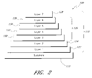
[0049] FIG. 2 is a schematic diagram of a multi-layer ophthalmic lens coating
in accordance with certain embodiments.
[0050] FIG. 3 is a schematic diagram of another multi-layer ophthalmic lens
coating in accordance with some embodiments.
DETAILED DESCRIPTION OF PREFERRED EMBODIMENTS
[0051] Although certain preferred embodiments and examples are disclosed
below, inventive subject matter extends beyond the specifically disclosed
embodiments to
other alternative embodiments and/or uses, and to modifications and
equivalents thereof.
-11-
CA 02793855 2012-09-20
WO 2011/119414 PCT/US2011/028892
Thus, the scope of the claims appended hereto is not limited by any of the
particular
embodiments described below. For example, in any method or process disclosed
herein,
the acts or operations of the method or process may be performed in any
suitable sequence
and are not necessarily limited to any particular disclosed sequence.
[00521 Various operations may be described as multiple discrete operations in
turn, in a manner that may be helpful in understanding certain embodiments;
however, the
order of description should not be construed to imply that these operations
are order
dependent. Additionally, the structures described herein may be embodied as
integrated
components or as separate components.
[0053] For purposes of comparing various embodiments, certain aspects and
advantages of these embodiments are described. Not necessarily all such
aspects or
advantages are achieved by any particular embodiment. Thus, for example,
various
embodiments may be carried out in a manner that achieves or optimizes one
advantage or
group of advantages as taught herein without necessarily achieving other
aspects or
advantages as may also be taught or suggested herein.
[0054] An antireflective coating for a lens can have a number of different
configurations. For example, an interference coating can have one or more thin
layers that
are configured to reduce reflections through destructive interference. In some
configurations, an antireflective interference coating has multiple layers
formed from
alternating low-refractive index and high-refractive index materials. A low-
refractive
index material such as silicon dioxide can be used to form one or more low-
index layers.
High-refractive index materials include metal oxides such as zirconium
dioxide, tantalum
pentoxide, and titanium dioxide, which can be used to form one or more high-
index
layers.
[0055] Some ARCs have low transmission, adhesion, and/or abrasion
resistance characteristics. For example, in some optical elements with a
synthetic resin,
the heating temperature in vapor deposition can be limited by the low melting
point of the
substrate. Because of this limitation, the density of the layers formed in
antireflection
layers may be lower than the optimal density, and the film refractivity and
abrasion
resistance of the film may suffer.
[0056] A polymeric optical element, such as a lens for eyewear, can include an
organic hard coat film formed on the plastic lens substrate for improving the
scratch
resistance of the coated lens. An inorganic antireflection film can be formed
on top of the
-12-
CA 02793855 2012-09-20
WO 2011/119414 PCT/US2011/028892
hard coat film. This AR coating method addresses mainly abrasion resistance
and possibly
adhesion. In some embodiments, a highly abrasion resistant lacquer disposed
between the
ARC and the substrate may not address all drawbacks of existing coating
technologies.
[0057] An ophthalmic lens can also have a hardening layer (for example,
Si02) of increased thickness in the AR stack. However, in some embodiments, an
increased thickness hardening layer, without other improvements, can induce
further
adhesion problems while increasing the abrasion resistance minimally. An
increased
thickness hardening layer may not improve the transmission of the lens.
[0058] In some embodiments, coating processes are configured to maintain
high transmission while improving abrasion resistance and adhesion of the
coating to a
finished lens. Coating processes can include one or more features, which, in
some cases,
can be combined with other disclosed features to provide further advantages.
[0059] Coating processes can be used to form an ARC on one or both sides of
an ophthalmic lens. In some embodiments, the ARC includes an increased
thickness
hardening layer. The hardening layer can be formed using physical vapor
deposition with
a suitable vapor source such as, for example, Si02. The thickness of the
hardening layer
can be greater than or equal to about 150 nm, greater than or equal to about
250 nm,
between about 150 nm and about 300 nm, between about 250 nm and 350 nm, about
300
nm, or another suitable thickness. The hardening layer can be deposited at a
rate that
allows the layer to form with substantial uniformity and high density.
[0060] The term "ophthalmic lens" is used herein in its broad and ordinary
sense. For example, ophthalmic lenses encompass corrective lenses, non-
corrective
lenses, tinted lenses, sunglass lenses, plastic lenses, glass lenses, and
other lenses used in
eyewear. The techniques and equipment used to make ophthalmic lenses has
typically
differed from the techniques and equipment used to make other types of lenses,
including
lenses used in precision optical systems.
[0061] The term "physical vapor deposition" is used herein in its broad and
ordinary sense. For example, the term encompasses coating techniques that
involve
physical processes in which a film is deposited by vacuum deposition on a
surface. The
term also encompasses coating techniques where a chemical or mechanical change
in the
coating material is induced by a directed energy source, such as an ion beam.
For
example, in some embodiments, the deposition surface may be activated
chemically by
exposure to ionized gases or reactive gases before or during physical vapor
deposition.
-13-
CA 02793855 2012-09-20
WO 2011/119414 PCT/US2011/028892
The term "physical vapor deposition" does not generally encompass chemical
vapor
deposition techniques as understood by one of ordinary skill in the art. For
example, the
term does not encompass a deposition technique wherein the deposition occurs
principally
by introducing a gas stream containing precursor gases outside of a plasma ion
source and
into the plasma ion beam. In physical vapor deposition, the material to be
deposited is
typically introduced into the deposition chamber in its solid phase and
vaporized.
[0062] An antireflective coating or stack can include a variety of materials,
including materials that are partially, mostly, nearly entirely, or entirely
transparent to
visible light. In some embodiments, the material system of an antireflective
stack is free
or mostly free of materials that absorb any substantial portion of visible
light. In certain
embodiments, the luminous transmittance of a clear polycarbonate lens coated
with an
antireflective stack described herein is greater than or equal to about 97%,
greater than or
equal to about 97.5%, about 98%, or greater than or equal to about 98%. In
some
embodiments, the luminous reflectance of the coated lens is less than about
4%, less than
about 3%, less than about 2.5%, or less than about 2%. The disclosed coatings
can be
applied to the convex surface, the concave surface, or both the convex and
concave
surfaces of a lens. In certain embodiments, the luminous reflectance of a
coated surface of
a lens is less than about 2%, less than about 1.5%, less than about 1%, or
less than about
0.5%. As used herein, luminous transmittance and luminous reflectance can be
measured
with respect to a standard daylight illuminant, such as CIE illuminant D65-
10063] In some embodiments, ion beam assisted deposition (IBAD) is used
during deposition of one or more layers of the antireflective stack. The term
"ion beam
assisted deposition" is used in its ordinary sense. For example, IBAD
encompasses thin
film deposition processes in which a substrate is exposed to a vapor phase
coating
material in a vacuum chamber. Any suitable vacuum chamber can be used,
including, for
example, the SatisLoh 1200 Box coater available from SatisLoh AG of Baar,
Switzerland.
During IBAD, individual coating atoms or molecules can condense on the
substrate to
form a coating. Simultaneously, an energetic ion beam is directed at the
substrate during
deposition of the coating material. In some embodiments, a different ion beam
power is
selected for different layers of the coating, and the ion beam can be
deactivated entirely
during deposition of one or more layers. In certain embodiments, the ion beam
power is
changed during deposition of a single layer.
-14-
CA 02793855 2012-09-20
WO 2011/119414 PCT/US2011/028892
[0064] The ion beam can be generated by an ion source. Any ion source
suitable for assisted deposition on an ophthalmic lens substrate can be used.
Examples of
such ion sources include an End Hall ion source, a Radio Frequency (RF) ion
source, and
an Anode Layer Source (ALS). The Mark II and Mark II+ Ion Sources, made by
Veeco
Instruments Inc. of Woodbury, New York, are examples of suitable End Hall ion
sources.
A suitable process gas can be used with the ion source. Process gasses can
include inert
gasses (e.g., argon, xenon, krypton, or neon), oxygen, reactive gasses, carbon-
bearing
gasses, other gasses, and combinations of gasses.
[0065] In the embodiment illustrated in FIG. 1 A, a pair of spectacles
includes
ophthalmic lenses 10a, 10b having at least one lens coating. The lenses 10a,
10b are
connected to a frame 12 that can have any suitable configuration. The
spectacles can be of
any type, including general-purpose eyewear, special-purpose eyewear,
sunglasses,
driving glasses, sporting glasses, indoor eyewear, outdoor eyewear, vision-
correcting
eyewear, contrast-enhancing eyewear, eyewear designed for another purpose, or
eyewear
designed for a combination of purposes.
[0066] FIG. 1B shows an embodiment of an ophthalmic lens 20 in which an
ophthalmic lens coating 24 is disposed on a convex surface of the lens body
substrate 22.
The thickness of the coating 24 is exaggerated in the drawings, and it is
understood that
the coating 24 can be much thinner than the lens body 22. The coating 24 can
include one
or more functional layer groups as described herein.
[0067] FIG. 1C shows an embodiment of an ophthalmic lens 30 in which an
ophthalmic lens coating 34 is disposed on a convex surface of the lens body
substrate 32
and another ophthalmic lens coating 36 is disposed on a concave surface of the
lens body
substrate 32. The relative thicknesses of the lens elements shown in FIG. 1C
are not
drawn to scale, and it is understood that each of the lens elements can have
any suitable
thickness. In some embodiments, each of the coatings 34, 36 can include one or
more
functional layer groups as described herein. Further, the coatings 34, 36 can
have
substantially the same composition or substantially different compositions.
The
configurations of each of the coatings 34, 36 can be selected to achieve any
desired
purpose or purposes, and a wide variety of possible configurations exist.
[0068] A lens can be coated with one or more functional layer groups. Each
functional layer group can include one or more layers, where "layer" is used
in its broad
and ordinary sense. For example, a layer can be a substantially contiguous
film deposited
-15-
CA 02793855 2012-09-20
WO 2011/119414 PCT/US2011/028892
from a single coating material or a single group of coating materials. In some
embodiments, each layer has a substantially uniform composition, although it
is
understood that variations in microstructure or morphology may occur within a
layer. The
functional layer groups can include, for example, a multilayer AR stack, a
hardening
layer, a topcoat layer, a hydrophobic layer, an anti-static layer, an adhesor
layer, another
functional layer, or a combination of layers. The AR stack can include a
plurality of high-
index layers and a plurality of low-index layers. Low refractive index layers
are made
from materials that typically have a refractive index of less than about 1.5
in the visible
spectrum, while high refractive index layers are selected from materials with
a refractive
index greater than the refractive index of at least one of the low-index
materials used in
the AR stack.
[0069] FIG. 2 shows a schematic diagram of the layers of an example coated
ophthalmic lens 100. The diagram shows the order of the coating layers 120 and
substrate
110 but does not indicate the thicknesses of the layers and substrate, which
are not drawn
to scale. The substrate 110 can be made from any suitable ophthalmic lens
material such
as, for example, polycarbonate, acrylic, resin, glass, another material, or a
combination of
materials. The substrate 110 can include one or more lens elements or other
structures.
The substrate 110 can also be hardcoated and/or have other surface treatments.
[0070] In the embodiment illustrated in FIG. 2, the coating 120 includes four
functional layer groups 122, 124, 126, 128. The first functional layer group
is an adhesor
layer 122 that is disposed on the substrate. The adhesor layer 122 can be made
from a
material system that can adhere the substrate 110 to the coating 120. The
material system
for the adhesor layer 122 can include Cr, SiO, Al2OX, Al, another suitable
material, or a
combination of materials. The thickness of the adhesor layer is generally
greater than or
equal to about 0.1 nm and/or less than or equal to about 10 nm. In some
embodiments, the
adhesor layer 122 material is a mixture of Cr and SiO, and the thickness of
the layer 122
is between about 0.6 nm and about 1 nm. The adhesor layer 122 can be deposited
without
using IBAD. Before the adhesor layer 122 is deposited, the substrate can be
cleaned by
providing a pulse of inert or reactive process gas to the deposition chamber
with the ion
source activated at low energy. Many other variations or alternative
configurations for the
adhesor layer 122 are possible.
[0071] In the embodiment illustrated in FIG. 2, a hardening layer 124 is
disposed on the adhesor layer 122. The hardening layer 124 can be an amorphous
layer of
-16-
CA 02793855 2012-09-20
WO 2011/119414 PCT/US2011/028892
silica with a thickness substantially greater than the other layers of the
coating 120. In
some embodiments, the hardening layer 124 includes a film of Si02 between
about 150
nm and about 300 nm thick. In certain embodiments, the thickness of the
hardening layer
is about 300 nm. Other configurations and thicknesses of the hardening layer
124 are
possible.
[0072] The hardening layer 124 can be deposited using IBAD, although some
coatings have a hardening layer 124 that is deposited without using IBAD. The
use of
IBAD during deposition of the hardening layer 124 is generally more preferred
when the
energy of the ion beam is relatively tunable and generally less preferred when
the ion
beam energy is less tunable or exhibits greater variability. For example, in
some
embodiments that use an End Hall source as the ion source, the hardening layer
124 is
deposited without using IBAD.
[0073] An antireflective (AR) stack 126 is disposed on the hardening layer
124. The AR stack 126 includes two high-index layers 130, 134 and two low-
index layers
132, 136. The high-index layers 130, 134 can be formed from a high-index
material such
as, for example, ZrO2. The low-index layers 132, 136 can be formed from a low-
index
material such as, for example, Si02. The thicknesses of the layers 130, 132,
134, 136 can
be selected to achieve maximum destructive interference of visible light
reflected at the
interfaces between the layers, thereby increasing visible light transmission.
[0074] In some embodiments, IBAD is used during deposition of only the
high-index layers 130, 134 in the stack 126. In at least some such
embodiments, the
stresses between high-index layers 130, 134 and low-index layers 132, 136 can
be at least
partially balanced than if IBAD were not used at all or if IBAD were used
during
deposition of both the high-index layers 130, 134 and the low-index layers
132, 136.
High-index layers of an AR stack can be compacted by IBAD, which makes the
microstructure of the layers more crystalline and increases the hardness of
the layers.
IBAD can also increase the oxidation of the high-index layers, which results
in greater
transparency.
[0075] Thin film layers that are at least partially balanced can include, for
example, first and second layers disposed adjacent to one another, where one
layer is
inherently negatively stressed and the other layer is inherently positively
stressed. In
certain embodiments, the first layer can have a level of inherent positive
stress that
substantially balances or at least partially balances the level of inherent
negative stress in
-17-
CA 02793855 2012-09-20
WO 2011/119414 PCT/US2011/028892
the compressively stressed layer. In some embodiments, when the stresses of
two or more
layers that are at least partially balanced are summed, the magnitude of the
result is less
than the magnitude of the highest level of stress in any of the two or more
layers alone. In
certain embodiments, when the stresses of two or more layers that are
substantially
balanced or at least partially balanced are summed, the magnitude of the
result is close to
zero or substantially equal to zero. In other embodiments, when the stresses
of two or
more layers that are at least partially balanced are summed, the magnitude of
the result is
not close to zero or substantially equal to zero.
[0076] The inherent stress in one or more layers of the coating shown in FIG.
2 can be varied using IBAD. In some embodiments, the energy level of the ion
beam
during IBAD can be selected to tune the inherent stress of a layer to better
balance the
stresses between the layer and adjacent layers. For example, IBAD can be used
during
deposition of a high-index Zr02 layer between compressively stressed, low-
index Si02
layers. In this example, the ion energy during deposition of the Zr02 layer
can be selected
to be about 100 eV when the layer is deposited at a rate of about 0.6 nm/s and
when
Argon is used as the process gas. The Zr02 layer can have an increased level
of inherent
stress compared to the low-index layers, resulting in a low level of overall
stress in the
stack and reduced local stresses at the upper and/or lower interfaces. In some
embodiments, the Zr02 layer can have a level of inherent positive stress that
substantially
balances or at least partially balances the level of inherent negative stress
in the
compressively stressed Si02 layers. In certain embodiments, only the high-
index layers of
a multilayer interference coating are deposited using IBAD. In certain such
embodiments,
all of the high-index layers are deposited using IBAD.
[0077] In the embodiment illustrated in FIG. 2, a topcoat layer 128 is
disposed
on the AR stack 126. The topcoat layer 128 can include a material system
configured to
impart one or more properties to the surface of the finished lens. For
example, the
material system of the topcoat layer 128 can include a hydrophobic material.
The
thickness of the topcoat layer 128 is typically between about 3 nm and about
25 nm,
although the thickness of the layer can depend largely on the material system
of the layer.
The topcoat layer 128 is typically deposited without using IBAD, although IBAD
made be
used during deposition of the topcoat layer 128 in certain embodiments. Many
configurations for the topcoat layer 128 are possible.
-18-
CA 02793855 2012-09-20
WO 2011/119414 PCT/US2011/028892
[0078] FIG. 3 shows a schematic diagram of the layers of another example
coated ophthalmic lens 200. The diagram shows the order of the coating layers
220 and
substrate 210 but does not indicate the thicknesses of the layers and
substrate, which are
not drawn to scale. The substrate 210 can be made from any suitable ophthalmic
lens
material such as, for example, polycarbonate, acrylic, resin, glass, another
material, or a
combination of materials. The substrate 210 can include one or more lens
elements or
other structures. The substrate 210 can also be hardcoated and/or have other
surface
treatments.
[0079] In the embodiment illustrated in FIG. 3, the coating 220 includes four
functional layer groups 222, 224, 226, 228. The first functional layer group
is an adhesor
layer 222 that is disposed on the substrate. The adhesor layer 222 can be made
from a
material system that can adhere the substrate 210 to the coating 220. The
material system
for the adhesor layer 222 can include Cr, SiO, A120x, Al, another suitable
material, or a
combination of materials. The thickness of the adhesor layer is generally
greater than or
equal to about 0.1 nm and less than or equal to about 10 nm. In some
embodiments, the
adhesor layer 222 material is a mixture of Cr and SiO, and the thickness of
the layer 222
is between about 0.6 nm and about 1 nm. The adhesor layer 222 can be deposited
without
using IBAD. Before the adhesor layer 222 is deposited, the substrate can be
cleaned by
providing a pulse of inert process gas to the deposition chamber with the ion
source
activated at low energy. Many other variations or alternative configurations
for the
adhesor layer 222 are possible.
[0080] A hardening layer 224 is disposed on the adhesor layer 222. The
hardening layer 224 can be an amorphous layer of silica with a thickness
substantially
greater than the other layers of the coating 220. In some embodiments, the
hardening layer
224 includes a film of Si02 between about 150 nm and about 300 nm thick. In
certain
embodiments, the thickness of the hardening layer 224 is about 300 nm. Other
configurations and thicknesses of the hardening layer 224 are possible.
[0081] The hardening layer 224 can be deposited using IBAD, although some
embodiments include coatings having a hardening layer 224 that is deposited
without
using IBAD. The use of IBAD during deposition of the hardening layer 224 is
generally
more preferred when the energy of the ion beam is relatively tunable and
generally less
preferred when the ion beam energy is less tunable or exhibits greater
variability. For
example, in some embodiments that use an End Hall source as the ion source,
the
-19-
CA 02793855 2012-09-20
WO 2011/119414 PCT/US2011/028892
hardening layer 224 is deposited without using IBAD. In some embodiments that
use a
tunable ion source, such as an RF source, the hardening layer 224 is deposited
using
IBAD. The ion energy used can be varied as deposition of the hardening layer
224
progresses from the lower interface to the upper interface. By varying ion
energy during
deposition, the inherent stresses within the layer 224 can be tailored to at
least partially
balance stresses in adjacent layers 222, 230. In some embodiments, the ion
energy used
increases as deposition proceeds from the lower interface towards the upper
interface of
the layer 224. The variation in ion energy can be gradual or can occur in one
or more
steps. The ion source can also be completely off during at least a portion of
the layer
deposition.
[0082] Some types of ion sources exhibit greater variability in the energy of
generated ions that other types of ion sources. An example of an ion source
that generates
ions with relatively high energetic variability is an End Hall source. The
energetic
variability of ions produced by an End Hall source can be substantially
higher, e.g., about
8 times higher (or about an order of magnitude higher) than the energetic
variability of
ions produced by an RF ion source. In other words, the energy of individual
ions emitted
by an End Hall source can vary substantially from the average ion energy
level. Thus, the
tunability and/or selectivity of an ion source may be less than desired.
Further, use of an
End Hall ion source with certain process materials, including silica, may
degrade the
performance or condition of the ion source. In some embodiments, using an RF
ion source
can mitigate or eliminate some of the drawbacks associated with ion sources
with high
energetic variability in general and with End Hall ion sources in particular.
[0083] An antireflective (AR) stack 226 is disposed on the hardening layer
224. The AR stack 226 includes a layer system with low- and high-index layers.
In the
embodiment shown in FIG. 3, the stack 226 includes multiple (e.g., two) high-
index
material regions and two low-index material regions. The first high-index
region is a
single layer 230 of high-index material. The second high-index region includes
more
layers than the first high-index region (e.g., four layers 234, 236, 238, 240)
having distinct
compositions of high-index material. The high-index regions alternate with two
single-
layer low-index regions 232, 242. The high-index layers 230, 234, 238, 240 can
be
formed from a high-index material such as, for example, Zr02, Ta2O5, a mixture
of
zirconium oxide and tantalum oxide, indium oxide, indium oxide doped with tin
oxide
(ITO), zinc oxide, zinc oxide doped with aluminum oxide (AZO), Nb205, a
blended
-20-
CA 02793855 2012-09-20
WO 2011/119414 PCT/US2011/028892
material, another material, or a combination of materials. The layer materials
within a
high-index region can be selected to improve the transmission, anti-static
characteristics,
and/or other properties of the coating 220. The low-index layers 232, 242 can
be formed
from a low-index material such as, for example, Si02, a mixture of Si02 and
A1203, a
blended material, another suitable material, or a combination of materials.
The
thicknesses of the layers 230, 232, 234, 236, 238, 240, 242 can be selected to
achieve high
destructive interference of visible light reflected at the interfaces between
the layers,
thereby increasing visible light transmission.
[0084] In some embodiments, IBAD is used during deposition of only the
layers 230, 234, 236, 238, 240 of the stack 226 made from high-index
materials. In certain
embodiments, the stresses between layers can be at least partially unbalanced
if IBAD is
not used at all or if IBAD is used during deposition of both the high-index
layers 230,
234, 236, 238, 240 and the low-index layers 232, 242. High-index layers of an
AR stack
can be compacted by IBAD, which makes the microstructure of the layers more
crystalline and increases the hardness of the layers. IBAD can also increase
the oxidation
of the high-index layers, which results in greater transparency. By using a
tunable ion
source capable of providing high ion energy levels, such as an RF source, the
composition
stoichiometry of the film layers can be controlled with precision. Further,
the density of
the layers deposited with IBAD can be substantially increased.
[0085] IBAD can also be used to improve the balance of stresses between
layers that have different levels of inherent stresses, thereby decreasing the
stress in an
overall stack. In a thin film layer deposited on a substrate, inherent stress
can vary along a
continuum extending from a tensile stressed state-where the layer is under
tension, a
stress state leading to expansion-to a compressively stressed state-where the
layer is
under compression. Thin films deposited without IBAD are typically
compressively
stressed at varying levels. As used herein, tensile stress will be called
"positive stress,"
while compressive stress will be called "negative stress." When tuning of
inherent stress
in a layer is discussed herein, it is understood that an "increase" in
inherent stress refers to
a change in the direction of increasing positive (i.e., tensile) stress and
decreasing
negative (i.e., compressive) stress.
[0086] Overall stress in a coating can be approximated by summing the
inherent stresses of the individual layers in the coating, while local stress
at an interface
between layers in the coating is at least partially influenced by the sum of
the inherent
-21-
CA 02793855 2012-09-20
WO 2011/119414 PCT/US2011/028892
stresses in the layers adjacent to the interface. Local stress can be reduced
or eliminated
when adjacent layers are generally balanced. As an example, two adjacent
layers are
generally balanced when the magnitude of positive stress in one layer is close
to the
magnitude of negative stress in the other layer.
[0087] The inherent stress in one or more thin film layers of the coating
shown
in FIG. 3 can be increased using IBAD. In some embodiments, the energy level
of the ion
beam during IBAD can be selected to tune the inherent stress of a layer to
better balance
the stresses between the layer and adjacent layers. For example, IBAD can be
used during
deposition of a high-index layer having a blended Zr-Ta-oxide composition
that, in its
final configuration, is disposed between compressively stressed, low-index
layers
comprising Si02. In this example, the ion energy during deposition of the high-
index layer
can be selected to be about 100-300 eV when the layer is deposited at a rate
of about 0.3
nm/s and when oxygen or an argon-oxygen blend is used as the process gas. The
resulting
high-index layer will have an increased level of inherent stress compared to
the same
high-index layer deposited without ion beam assisted deposition, thereby
lowering overall
stress in the stack and reducing local stresses at the upper and/or lower
interfaces. In some
embodiments, a high-index layer deposited using IBAD can have a level of
inherent
positive stress that is substantially balanced or at least partially balanced
with the level of
inherent negative stress in the compressively stressed low-index layers. In
certain
embodiments, only the high-index layers of a multilayer interference stack are
deposited
using IBAD. In certain such embodiments, all of the high-index layers are
deposited using
IBAD.
[0088] A graduated IBAD technique can be used to vary the energy level of
the ion beam during deposition of a single layer. When such a technique is
used, the stress
at the upper interface of the layer can at least partially balance the stress
in the above
adjacent layer and the stress at the lower interface of the layer can at least
partially
balance the stress in the below adjacent layer, even when the inherent
stresses in the
above adjacent and below adjacent layers are different. By varying the energy
level of the
ion beam within at least a portion of the range of energy levels at which an
ion source can
operate, a layer may be deposited such that a substantial inherent stress
gradient exists
within the deposited layer. In some embodiments, a graduated IBAD technique is
used
during deposition of one or more high index layers. In certain embodiments,
the graduated
IBAD technique is used during deposition of each of the high index layers. In
some
-22-
CA 02793855 2012-09-20
WO 2011/119414 PCT/US2011/028892
embodiments, the graduated IBAD technique is used during deposition of a
hardening
layer. Many other variations are possible, and it is understood that the
graduated IBAD
technique may be advantageously used during deposition of other layers of a
lens coating.
[0089] The use of IBAD during deposition of a layer can also increase the
density of the layer. The density of the layer can increase with higher ion
beam energy
levels through at least a portion of the range of energy levels that an ion
source can
produce. Some ion sources may have a greater range of possible energy levels
than other
ion sources. For example, a typical RF ion source has the capability of
operating at higher
ion beam energy levels than a typical End Hall source. By varying the energy
level of the
beam within at least a portion of the range of energy levels at which an ion
source can
operate, a layer may be deposited such that a substantial density gradient
exists within the
deposited layer.
[0090] In the embodiment illustrated in FIG. 3, a topcoat layer 228 is
disposed
on the AR stack 226. The topcoat layer 228 can include a material system
configured to
impart one or more properties to the surface of the finished lens. For
example, the
material system of the topcoat layer 228 can include a hydrophobic material.
The
thickness of the topcoat layer 228 is typically between about 3 nm and about
25 nm,
although the thickness of the layer can depend largely on the material system
of the layer.
The topcoat layer 228 is typically deposited without using IBAD, although IBAD
made be
used during deposition of the topcoat layer 228 in certain embodiments. Many
configurations and application methods for the topcoat layer 228 are possible.
Example coating configurations
[0091] A first example coating configuration for a polycarbonate ophthalmic
lens is shown in Table A. The structure of the example configuration is
similar in many
respects to the embodiment shown in FIG. 2, and the functional layer groups in
the table
are identified by corresponding reference numbers. Additional details
regarding the layer
materials, the thickness of each layer, the rate of deposit for each layer,
whether IBAD is
used during deposition of a layer, the ion energy of an End Hall ion source,
and the
process gas are provided in this example. The example also provides details
for a clean
step that can take place prior to deposition of the adhesor layer. During the
clean step, the
substrate can be contacted with ionized species of an inert gas, a reactive
gas, or a mixture
inert gas and reactive gas. In this example, the deposition process begins
with the clean
step and proceeds in order with deposition of the layers beginning with the
adhesor layer
-23-
CA 02793855 2012-09-20
WO 2011/119414 PCT/US2011/028892
122 (nearest the ophthalmic lens) and ending with the topcoat layer 128
(furthest from the
ophthalmic lens).
Table A
Functional Layer material Thickness Use Ion energy
layer group Rate of deposit IBAD? Process gas
Hydrophobic 3 nm - 25 nm
Topcoat 128 No N/A
material system 0.2 nm/s
90 run
Si02 No N/A
1.3 nm/s
56 nm 100 eV
Zr02 Yes
Antireflective 0.6 nm/s Argon
stack 126 32.67 nm
Si02 No N/A
1.3 nm/s
28nm 100 eV
Zr02 Yes
0.6 nm/s Argon
Hardening layer 300 nm
Si02 No N/A
124 1.3 nm/s
Adhesor layer Mixture of Cr 0.6 - 1.0 nm
No N/A
122 and SiO 0.02 nm/s
60 eV
Clean step N/A N/A No
Argon
[0092] Certain advantages and features of the example coating configuration
will now be discussed. The advantages that will be discussed are believed to
be at least
partially attributable to one or more aspects of the example coating
configuration
disclosed above. Some embodiments include these advantages. For example, the
use of
IBAD during the deposition of the high-index layers provides a very dense high-
index
material and also produces a very repeatable and controllable refractive index
for the
high-index layers. It has been observed that the abrasion resistance of a lens
coated with
the example coating configuration is substantially increased when compared to
other
coated ophthalmic lenses.
-24-
CA 02793855 2012-09-20
WO 2011/119414 PCT/US2011/028892
[0093] Among techniques for measuring abrasion resistance, an industry
standard testing procedure known as the Tumble Abrasion Test, designed by
Colts
Laboratories of Clearwater, Florida, is particularly rigorous and applicable
to the
determination of the abrasion resistance of a coated lens. The Tumble Abrasion
Test is
described in a Tumble Abrasion Standard Operating Procedure document published
by
Colts Laboratories on November 13, 2009. The document explains that a value
known as
the "Tumble Average Ratio" can be determined by performing a hazemeter
evaluation of
a Colts Standard Control Lens available from Colts Laboratories and a sample
lens after
both lenses are subjected to abrasion.
[0094] The Tumble Abrasion Test is used to test sample lenses that are within
a power range of -0.50 to +0.50 diopters, have front (convex) curves within +/-
0.25
diopters of control lenses, and have weight and diameter equivalent to the
control lenses.
The test is designed to provide comparative abrasion damage to sample and
control
lenses. Up to six test lenses and two control lenses may be tested in a single
test run using
the same abrasive mix. Test and control lenses are conditioned by exposing
them to
laboratory conditions for at least 24 hours before testing.
[0095] A new batch of abrasive media is prepared for each group of lenses that
is tested using the Tumble Abrasion Test. A certain amount of each media
component is
counted or weighed, and the media components are combined in a hexagonal
Rampart
RB-2 Vinyl lined tumble barrel attached to a Rampart RBD-1 Tumble Machine. The
media that are loaded into the tumble barrel are: 12 pieces of 3M Scrub pads
cut into
triangular shapes measuring 10.16 x 15.24 1.27 cm, 20 pieces of white
polyurethane
foam cut into triangular shapes measuring 10.16 x 15.24 1.27 cm, 459 15
grams of
whole-wheat bran, 28 2 grams of #4 cube sawdust, 100 3 grams of 40/60 mesh
grit-o-
cob, 145 5 grams of 20/40 mesh grit-o-cob, 130 4 grams of white silica
sand, and 72
3 grams of #12 emery. The media are mixed prior to sample abrasion by placing
a cover
over the tumble barrel filled with media and running the tumble machine at 29
rpm 1.
After 10 minutes of mixing, the tumble machine is stopped and the material
laying under
the cover is pushed back into the tumble barrel.
[0096] An identifier is scribed on an appropriate side of the lenses no more
than 10 mm from the edge of the lens. For convex side testing, the identifier
is scribed on
the concave side of the lens. The lenses are then washed. The initial haze of
the standard
-25-
CA 02793855 2012-09-20
WO 2011/119414 PCT/US2011/028892
control lenses and test lenses are read using a BYK-Gardener Haze-Gard Plus or
equivalent. In order to test the convex side, a two-inch piece of black
electrical tape is
placed on the concave side of the lens so that only the convex side of the
lens is abraded.
The test samples and standards are weighed. The weight of each lens should be
within
25% of the weight of each other lens. Electrical tape can be added to adjust
the weight of
individual lenses. The test samples and standards are placed randomly into the
tumble
barrel, which is tumbled for 20 minutes at 29 rpm 1. After tumbling is
completed, the
lenses are carefully removed from the tumble barrel, and the tape is removed
from the
lenses. The concave side of each lens is wiped with alcohol to remove any tape
residue.
The lenses are washed before reading the final haze and photographing the
lenses.
[0097] The Tumble Average Ratio is calculated by finding the difference
between the final haze value and the initial haze value for each standard lens
and for each
test lens, finding the average difference in haze value for the standard
lenses (average
standard lens haze gain) and the test lenses (average test lens haze gain),
and dividing the
average standard lens haze gain by the average test lens haze gain.
[0098] Five batches of polycarbonate lenses employing the example coating
configuration were subjected to the Tumble Abrasion Test, and the convex-side
Tumble
Average Ratio of each batch was calculated. The convex-side Tumble Average
Ratios of
three commercial coating products on polycarbonate lenses, as determined by
Colts
Laboratories, are also shown as comparative examples. The transmittance
percentages for
the example coating configuration and the comparative examples were also
determined.
-26-
CA 02793855 2012-09-20
WO 2011/119414 PCT/US2011/028892
The results are shown in Table B.
Table B
Coating configuration Tumble Average Ratio Transmittance %
Example coating, batch 1 10.74 97.88
Example coating, batch 2 8.12 97.66
Example coating, batch 3 7.39 97.61
Example coating, batch 4 9.35 97.73
Example coating, batch 5 9.86 97.64
Comparative example: 4.5 97.1
Product A
Comparative example: 3.39 97.7
Product B
Comparative example: 4.33 97.83
Product C
[0099] The results in Table B show that each of the polycarbonate' lenses with
the example coating configuration had a Tumble Average Ratio greater than 7,
while each
of the comparative polycarbonate lens examples had a Tumble Average Ratio less
than 5.
Significantly, the mean Tumble Average Ratio for the five example coating
configuration
batches was about 9, more than twice the Tumble Average Ratio of the
comparative
examples.
[0100] The increase in abrasion resistance was achieved without substantial
lowering of the lens transmittance. The use of IBAD during deposition of the
high-index
layers can result in a fully oxidized high-index material. Fully oxidized high-
index
materials exhibit higher transmittance compared to partially oxidized high-
index
materials.
[0101] The use of IBAD during deposition of the high-index layers permits
modification of the inherent stress of those layers. The materials in the
example coating
configuration were chosen to have opposing inherent stresses: in particular,
Si02 is
compressively stressed, and Zr02 is tensile stressed or at least less
compressively stressed
than Si02. The inherent stresses of the example coating configuration's layers
were
-27-
CA 02793855 2012-09-20
WO 2011/119414 PCT/US2011/028892
configured to balance or at least partially balance the stresses within the AR
stack,
resulting in a very durable and impact resistant product.
[0102] The thickness of the hardening layer in the first example coating
configuration is greater than the thickness of the hardening layers in many
existing
ophthalmic lens coating products. As the inherent stress of a layer is
positively correlated
with the thickness of the layer, there is a greater potential stress imbalance
compared to
those existing products. The inherent stress of the high-index layers was
tuned using
IBAD to balance the compressive stress of the Si02 layers in order to at least
partially
balance the overall stress of the coating. A more stress-balanced coating
typically exhibits
better adhesion, abrasion resistance and impact resistance than an otherwise
similar less
stress-balanced coating.
[0103] Adhesion of lenses employing the example coating configuration was
tested using the CHOCA and Salt Water Boil Tests with no failures. Impact
strength of
the lenses was also tested with no failures at 1927 inches of drop height,
which was the
maximum capability of the test instrument employed to test impact strength.
[0104] A second example coating configuration for a polycarbonate
ophthalmic lens is shown in Table C. The structure of the example
configuration is
similar in many respects to the embodiment shown in FIG. 3, and the functional
layer
groups in the table are identified by corresponding reference numbers.
Additional details
regarding the layer materials, the thickness of each layer, the rate of
deposit for each layer,
whether IBAD is used during deposition of a layer, the ion energy of an RF ion
source,
and the process gas are provided in this example. The example also provides
details for a
clean step that can take place prior to deposition of the adhesor layer.
During the clean
step, the substrate can be contacted with ionized species of an inert gas, a
reactive gas, or
a mixture inert gas and reactive gas. In this example, the deposition process
begins with
the clean step and proceeds in order with deposition of the layers beginning
with the
adhesor layer 222 (nearest the ophthalmic lens) and ending with the topcoat
layer 228
(furthest from the ophthalmic lens).
-28-
CA 02793855 2012-09-20
WO 2011/119414 PCT/US2011/028892
Table C
Functional Layer material Thickness Use Ion energy
layer group Rate of deposit IBAD? Process gas
Hydrophobic 3 nm - 25 rim
Topcoat 228 No N/A
material system 0.2 nm/s
72nm
Si02 No N/A
1.3 nm/s
4nm 100 eV
ITO (anti-static) Yes
0.05 nm/s O2 or Ar/02
33 nm 100-300 eV
Zr-Ta-oxide Yes
0.45 nm/s O2 or Ar/02
Antireflective 63 nm 100-300 eV
Nb205 Yes
stack 226 0.30 nm/s 02 or Ar/02
61 nm 100-300 eV
Zr-Ta-oxide Yes
0.45 nm/s O2 or Ar/02
52 nm
Si02 No N/A
1.3 nm/s
8 nm 100-300 eV
Zr-Ta-oxide Yes
0.30 nm/s 02 or Ar/02
Hardening layer Si02 150-300 nm Yes 100-150 eV
224 1.3 nm/s 02 or Ar/02
Adhesor layer Mixture of Cr 0.6 - 1.0 rim
No N/A
222 and SiO 0.02 nm/s
60 eV
Clean step N/A N/A No
Argon
[0105] Certain advantages and features of the example coating configuration
shown in Table C will now be discussed. The advantages that will be discussed
are
believed to be at least partially attributable to one or more aspects of the
example coating
configuration disclosed above. For example, the use of IBAD during the
deposition of the
high-index layers can provide a very dense high-index material and also
produces a very
repeatable and controllable refractive index for the high-index layers. It has
been observed
-29-
CA 02793855 2012-09-20
WO 2011/119414 PCT/US2011/028892
that the abrasion resistance of a lens coated with the example coating
configuration is
substantially increased when compared to existing coated plastic lenses.
[0106] The use of IBAD during deposition of the high-index layers permits
modification of the inherent stress of those layers. The materials in the
example coating
configuration were selected such that inherent stresses of adjacent layers are
at least
partially balanced. For example, the low index Si02 layers are compressively
stressed, and
the high index layers are tensile stressed or at least less compressively
stressed than the
Si02 layers. The inherent stresses of at least some layers of the example
coating
configuration can be increased using IBAD to balance or at least partially
balance the
stresses within the coating, resulting in a very durable and impact resistant
product.
[0107] The thickness of the hardening layer in the second example coating
configuration is greater than the thickness of the hardening layers in many
existing
ophthalmic lens coating products. Because the inherent stress of a layer is
positively
correlated with the thickness of the layer, there is a greater potential
stress imbalance
compared to the stress imbalances in existing products. In some embodiments,
the
inherent stress of the high-index layers is tuned using IBAD to at least
partially balance
the compressive stress of the Si02 layers in order to achieve a coating with a
low level of
overall stress. A more stress-balanced coating typically exhibits better
adhesion, abrasion
resistance and impact resistance than a less stress-balanced coating that is
otherwise
similar in many respects to the example coating configuration.
[0108] It is contemplated that the particular features, structures, or
characteristics of any embodiments discussed herein may be combined in any
suitable
manner in one or more separate embodiments not expressly illustrated or
described. For
example, it is understood that a coating can include multiple antireflective
stacks and that
a combination of functional layer groups can combine to provide antireflective
functionality. It is further understood that one or more features of the first
example
coating configuration can be combined with one or more features of the second
example
coating configuration, resulting in numerous additional lens coating
embodiments, which
are part of this disclosure.
[0109] In many cases, structures that are described or illustrated as unitary
or
contiguous can be separated while still performing the function(s) of the
unitary structure.
In many instances, structures that are described or illustrated as separate
can be joined or
combined while still performing the function(s) of the separated structures.
It is further
-30-
CA 02793855 2012-09-20
WO 2011/119414 PCT/US2011/028892
understood that the coatings disclosed herein may be used in at least some
lens
configurations and/or optical systems besides ophthalmic lenses.
[01101 It should be appreciated that in the above description of embodiments,
various features are sometimes grouped together in a single embodiment,
figure, or
description thereof for the purpose of streamlining the disclosure and aiding
in the
understanding of one or more of the various inventive aspects. This method of
disclosure,
however, is not to be interpreted as reflecting an intention that any claim
require more
features than are expressly recited in that claim. Moreover, any components,
features, or
steps illustrated and/or described in a particular embodiment herein can be
applied to or
used with any other embodiment(s). Thus, it is intended that the scope of the
inventions
herein disclosed should not be limited by the particular embodiments described
above, but
should be determined only by a fair reading of the claims that follow.
-31-