Note: Descriptions are shown in the official language in which they were submitted.
CA 02794493 2012-10-26
KEY ASSEMBLY FOR ELECTONIC DEVICE
TECHNICAL FIELD
[0001] The present disclosure relates to electronic devices, and, more
particularly, to
key assemblies for electronic devices.
BACKGROUND
[0002] Electronic devices often have a number of physical keys which may be
used
for inputting instructions to such devices. In order to facilitate use of
electronic devices in
low lighting conditions, electronic devices sometimes backlight such physical
keys. When
backlighting keys, an effect known as light leak may sometimes occur. Light
leak occurs
when light is emitted from undesirable portions of the electronic device. This
can result in
unbalanced and unattractive backlighting of keys.
[0003] To avoid having to provide a light source beneath every key, the light
from a
light source (e.g. a light emitting diode) is guided to multiple keys. In some
devices, a light
guide foil is positioned underneath a set of keys and the light guide foil
functions to spread
out the light from the light source. In some cases, a side-fire LED or similar
source is used to
inject light into the foil. However, side-fire LEDs tend to be costly. Top-
fire LEDs are thus
sometimes used as a light source to inject light into the foil; however, this
arrangement
presents difficulties when designing to ensure a shallow depth to the key
assembly.
BRIEF SUMMARY
[0004] In one aspect, the present disclosure describes a key assembly for an
electronic
device. The key assembly includes an optical radiation source having a surface
through
which light is emitted, in use; a mask blocking a portion of the light emitted
by the optical
radiation source, in use; a light guide; and a keycap, defining a key, the
keycap having a non-
opaque portion; and wherein the mask is located between the surface and the
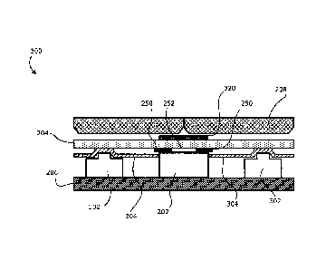
light guide, and
the light guide is located between the mask and the keycap, such that the
keycap receives
optical radiation emitted from the optical radiation source that is not
blocked by the mask.
CA 02794493 2012-10-26
[0005] In another aspect, the present application describes electronic
devices that
incorporate the key assembly described herein.
[0006] Other example embodiments of the present disclosure will be apparent
to
those of ordinary skill in the art from a review of the following detailed
description in
conjunction with the drawings.
[0007] Although the description herein refers to light emitting diodes
(LEDs), the
present application is applicable to optical radiation sources more generally
and is not
necessarily limited to LEDs in particular.
BRIEF DESCRIPTION OF THE DRAWINGS
[0008] Reference will now be made, by way of example, to the accompanying
drawings which show example embodiments of the present disclosure, and in
which:
[0009] FIG. 1 is a front perspective view of an example electronic device
having a
key lighting assembly in accordance with example embodiments of the present
disclosure;
[0010] FIG. 2 diagrammatically illustrates a cross-sectional view of a
portion of an
example key assembly;
[0011] FIG. 3 illustrates a cross-sectional view of a portion of another
example key
assembly;
[0012] FIG. 4 shows a top view of a top-fire LED, including its housing and
top
surface;
[0013] FIG. 5 shows the top view of FIG. 4 with an opaque mask affixed to
the top
surface;
[0014] FIG. 6 shows a cross-sectional view of a portion of a simplified
example
stack-up for a key assembly; and
[0015] FIG. 7 shows an exploded view of the portion of the simplified
example key
assembly of FIG. 6; and
2
CA 02794493 2012-10-26
[0016] FIG. 8 shows a cross-sectional view of a portion of another example
stack-up
for a key assembly.
[0017] Like reference numerals are used in the drawings to denote like
elements and
features.
DETAILED DESCRIPTION OF EXAMPLE EMBODIMENTS
[0018] Reference is now made to FIG. 1, which shows a perspective view of an
example electronic device 100. In the example embodiment shown, the electronic
device 100
is a handheld mobile communication device. However, the teachings described
herein may
be applied to other electronic devices. Such electronic devices may, in
various example
embodiments, include portable electronic devices such as mobile communication
devices,
including pagers, smartphones, cellular phones, global positioning system
(GPS) navigation
devices and other satellite navigation devices, wireless organizers, wireless
personal digital
assistants (PDA), desktop, netbook and notebook computers and tablet
computers. The
electronic devices may, in various embodiments, be devices without wireless
communication
capabilities such as PDAs, electronic gaming devices, digital photograph
albums or picture
frames, digital cameras or digital video recorders. These examples are
intended to be non-
limiting.
[0019] The electronic device 100 includes a housing 102 which contains various
electronic components which control operation of the electronic device 100.
Such electronic
components may include, for example, one or more processors. Other example
electronic
components which may be housed in the housing 102 will be discussed in greater
detail
below.
[0020] In some example embodiments, the electronic device 100 includes a
physical
keyboard or keypad 104. The keyboard or keypad 104 may be an alphanumeric
keyboard or
keypad which facilitates entry of alphanumeric characters into the electronic
device 100. In
at least some example embodiments, the keyboard or keypad 104 may be a QWERTY
or
DVORAK keyboard. The keyboard or keypad 104 includes a plurality of keys which
are
actuatable by a user to provide inputs to the electronic device 100.
3
CA 02794493 2012-10-26
[00211 In the example embodiment, the physical keyboard or keypad 104 is
exposed
by the housing 102 through a front surface of the housing 102. However, other
keyboard or
keypad 104 orientations are also possible. For example, in some example
embodiments, the
keyboard or keypad 104 is a sliding keyboard or foldout keyboard which is
movable between
an exposed position in which keys of the keyboard or keypad 104 are exposed
and a protected
position in which keys of the keyboard or keypad 104 are protected. That is,
in the protected
position, the keys of the keyboard or keypad 104 are hidden by other features
of the
electronic device 100. In yet other example embodiments (not illustrated), the
electronic
device 100 may be an electronic device which does not include a physical
keyboard or
keypad 104. Instead, alphanumeric input may be achieved through the use of a
virtual
keyboard displayed on a touchscreen of the electronic device 100.
[0022] The housing 102 houses a display assembly 120. In the example
embodiment
illustrated, the display assembly 120 is disposed within the housing 102
facing the same
direction as the keyboard or keypad 104. More particularly, in the example
embodiment
illustrated, the electronic device 100 is oriented in a portrait orientation
in which a left side
142 and a right side 140 of the electronic device 100 are longer than a top
side 144 and a
bottom side 146 of the electronic device 100. In this orientation, the key and
display
assembly 120 is disposed above the keyboard or keypad 104. That is, the key
and display
assembly 120 is located closer to the top side 144 than is the keyboard or
keypad 104. In this
orientation, the keyboard or keypad 104 is actuatable by a user's thumbs when
the device 100
is cradled in a user's hands. It will be appreciated that this is an example
orientation and that
other configurations are possible.
[0023] The display assembly 120 includes a display cover 152, which may also
be
referred to as a lens. The display cover 152 is transparent, permitting users
to view the
display screen, which is disposed beneath the display cover 152. The display
cover 152
protects components disposed there below and inhibits debris and other
contaminants from
entering the electronic device 100. The display screen displays information in
response to
commands from one or more processors within the electronic device 100. The
display cover
152 may include a touchscreen overlay for accepting touch screen inputs in one
embodiment.
The display screen may be, in some example embodiments, a liquid crystal
display (LCD)
module. Alternatively, in at least some example embodiments, the display
screen may be
4
CA 02794493 2012-10-26
another type of display device, such as an organic light emitting diode (OLED)
module, a
plasma display panel (PDP) module, or the like.
[0024] Between the display assembly 120 and the keyboard or keypad 104 is
disposed
a function key assembly 193. The key assembly 193 includes a keycap 150
defining one or
more function keys 106a, 106b, 106c, 106d. In one embodiment, the keycap 150
may be
integrally formed with the display cover 152. In some embodiments, the keycap
150 is a
separate element from the display cover 152. In yet other embodiments, the
keycap 150 is
formed as multiple keycaps; for example, one keycap for each function key 106,
or one
keycap for each pair of function keys.
[0025] The function keys 106a, 106b, 106c, 106d are configured to be
depressed by a
user of the electronic device 100 to input commands to the electronic device
100. In the
example illustrated, there are four function keys 106 which are disposed
horizontally between
the left side 142 and the right side 140 of the electronic device 100. The
function which is
assigned to each function key 106a, 106b, 106c, 106d by the electronic device
100 may, in at
least some example embodiments, vary based on the operating state of the
electronic device
100. In the illustrated embodiment, the function keys 106a, 106b, 106c, 106d
include a first
function key 106a, which may be a send key which may be used to input a
command to
initiate communications on the electronic device 100. In the illustrated
example embodiment,
the function keys 106a, 106b, 106c, 106d also include a second function key
106b, which
may be a menu key which may be used to input a command to display a menu on a
display
screen of the electronic device 100. In the illustrated example embodiment,
the function keys
106a, 106b, 106c, 106d also include a third function key 106c, which may be an
escape key,
and which may also be referred to as a back key. The escape key may be used to
input a
command to exit from an application, module or state or to input a command to
return to a
previous state, such as a previously viewed web page. In the illustrated
example
embodiment, the function keys 106a, 106b, 106c, 106d also include a fourth
function key
106d, which may be an end or power key. The end or power key may be used to
input a
command to terminate an operating state, module or application running on the
electronic
device 102. For example, the end or power key may be used to input a command
to hang-up
a call or to input a command to power down the electronic device 100.
5
CA 02794493 2012-10-26
[0026] The function keys 106a, 106b, 106c, 106d each include one or more
decorations 156a, 156b, 156c, 156d on the external surface of the keycap 150.
The
decorations 156a, 156b, 156c, 156d are comprised of icons, text, images, or
other indicia
which identify a function assigned to the function key 106a, 106b, 106c, 106d
associated with
that decoration 156a, 156b, 156c, 156d. For example, in the example embodiment
illustrated,
a telephone icon is used to represent the send key, the letter "M" is used to
represent the
menu key, a back arrow icon is used to represent the escape key, and an on-
cradle telephone
icon is used to represent the end or power key. The decorations 156a, 156b,
156c, 156d are
each associated with one of the function keys 106a, 106b, 106c, 106d. For
example, a first
decoration 156a may be associated with the first function key 106a, a second
decoration 156b
may be associated with the second function key 156b, a third decoration 156c
may be
associated with the third function key 156c and a fourth decoration 156d may
be associated
with the fourth function key 156d.
[0027] The keycap 150 may be cantilever mounted at a first end 190 of the
keycap
150. That is, the keycap 150 is supported at the first end 190 of the keycap
150. The first
end 190 of the keycap 150 is the end of the keycap 150 which is nearest to the
display cover
152. In the example illustrated, the keycap 150 and the display cover 152 may
be a single
component, which may be referred to as an integrated keycap/display cover.
[0028] Although not visible in FIG. 1, the key assembly 193 generally
includes one or
more electrical switches mounted within the housing 102 beneath the keycap
150. The
electrical switches mounted beneath the keycap 150 are each associated with
corresponding
function keys 106a, 106b, 106c, 106d. The electrical switches are connected to
one or more
controllers, such as one or more processors associated with the electronic
device 100 and
provide input signals to the processors. The electrical switches are each
associated with and
aligned with corresponding keys.
[0029] Where the keycap 150 is cantilever mounted at the first end 190 of the
keycap
150, the keycap 150 may deflect at its second end 192, which is opposite the
first end 190, in
response to the application of an external force on the external surface of
the keypad. When
such a deflection occurs, the keycap 150 may actuate the electrical switch
which is associated
with the portion of the keycap where the external force was applied. In at
least some example
embodiments, the electrical switches are disposed beneath the second end 192
of the keycap.
6
CA 02794493 2012-10-26
[0030] In the example embodiment illustrated, the electrical switches may be
located
in a position which permits them to be actuated by a portion of the keycap
which is located
between the second end 192 and the decorations 156a, 156b, 156c, 156d. By
locating the
electrical switches in this position, the space beneath the decorations 156a,
156b, 156c, 156d
on the keycap 150 is not obstructed by the electrical switches. Locating the
electrical
switches away from the decorations 156a, 156b, 156c, 156d facilitates
backlighting of the
keycap 150. The electrical switches may be dome switches, in some embodiments.
[0031] The embodiment illustrated in FIG. 1 shows a single piece keycap 150
that
includes a plurality of function keys 106a, 106b, 106c, 106d. When a force is
applied to the
keycap 150 at one of the function keys 106a, 106b, 106c, 106d, there may be a
tendency for
an adjacent key to also depress, thereby engaging its associated electrical
switch.
Accordingly, the key assembly may include features which prevent or inhibit
movement of
keys 106a, 106b, 106c, 106d, when the adjacent key is depressed. Such features
may include,
for example, indentations or grooves (not shown) on the interior surface of
the keycap 150
between keys 106a, 106b, 106c, 106d which allows the keycap 150 to bend.
[0032] The electronic device 100 may include additional input devices in
addition to
the input devices discussed above. In the example embodiment of FIG. 1, the
electronic
device 100 includes a navigational input device 180. In the illustrated
embodiment, the
keycap 150 defines a passageway through which the navigational input device
180 extends.
The navigational input device 180 may be comprised of a trackpad. In other
embodiments,
the navigational input device 180 may be a trackball. Other navigational input
devices 180
are also possible. In some cases, no navigational device may present in this
location.
[0033] Reference is now made to FIG 2, which diagrammatically illustrates a
cross-
sectional view of a portion of an example key assembly 200. For clarity, only
some elements
of a typical key assembly are illustrated in FIG. 2. The portion of the key
assembly 200
includes an optical source, which in this example is a top-fire LED 202. The
LED 202 is
mounted or attached to a subsurface, such as a printed circuit board (PCB) 206
or other such
substrate. The portion of the key assembly 200 includes a light guide 204
under a keycap
208. The LED 202 is spaced from the underside of the light guide 204 by a
distance D. The
light guide may include a light guide foil, such a polycarbonate or other type
of moldable
flexible plastic, or any other type of light guide, including hard-plastic
light guides.
7
CA 02794493 2012-10-26
[0034] The LED 202 emits light upwards generally directed towards the light
guide
204. The light guide 204 functions to disperse the light such that the light
that passes through
the light guide 204 towards the keycap 208 is more uniformly distributed than
the light
incident on the underside of the light guide 204. The keycap 208 may be
structured to permit
at least a portion of light incident on its underside to pass through and exit
through a
decoration or diagram on its upper surface (not shown), thereby illuminating
(backlighting)
the decoration. In general, the keycap 208 is structured to prevent light from
exiting surfaces
of the keycap other than through the decoration. This may be accomplished
using foils,
paints, or other techniques applied to the surface of the keycap 208 in some
embodiments.
The decorations and/or diagrams are non-opaque portions of the keycap 208.
[0035] Reference is now made to FIG. 3 and FIG. 4. FIG. 3 shows another
embodiment of a portion of an example key assembly 300. In the example shown
in FIG. 3,
the key assembly 300 is constructed such that there is no gap between the LED
202 and the
light guide 204. This may advantageously reduce the thickness of the key
assembly 300,
thereby enabling the creation of thinner electronic devices.
[0036] FIG. 4 shows a top view of the top-fire LED 202. The LED 202 includes a
housing 216, the edges of which are visible in the illustration, and a top
surface 218 through
which the LED 202 emits light. It will be noted, that the LED 202 is
rectangular in structure
with two long sides 220 and two short sides 222. The light emitted from the
top-fire LED
202 is not a uniform spectrum across the entire top surface of the LED 202.
The light emitted
from the center portion of the LED 202 tends to be broad spectrum white light
(generally
indicated by reference number 210), whereas the areas furthest from the
center, particularly
near the short sides 222, tend to emit light that has a yellow tint (generally
indicated by
reference numbers 212 and 214). Although the present example depicts a
rectangular LED,
the present application is not limited to rectangular LEDs. The problem of
skewed colour
spectrum at the edges of the LED top surface is particularly noticeable in
rectangular LEDs,
but can also occur in other shaped LEDs, including square and even round LEDs.
[0037] The yellow tinted light at the edges of the top surface 218 tends to
become
visible when a reflector is placed in front of the LED top surface 218, such
that a portion of
the light emitted from the LED 202 is reflected back into the LED 202, causing
the yellow-
tinted areas of the LED to become more illuminated and, thus, to cause the
light that
8
CA 02794493 2012-10-26
eventually leaves the LED 202 to appear yellower at its edges. In a key
assembly, like key
assembly 200 (FIG. 2), in which the LED 202 is spaced apart from the light
guide 204 by a
distance D, the light emitted from the central portion of LED 202 does not
significantly
reflect back into the LED and does not significantly illuminate the more
yellow portions of
the LED top surface 218. Accordingly, the yellowish light 212, 214 does not
appear in the
configuration shown in FIG. 2.
[0038] In the key assembly 300 the LED 202 is in direct contact with the
underside of
the light guide 204, and the light emitting from the LED 202 is directly
injected into the light
guide 204. The net effect is an uneven dispersal of light within the light
guide 204, such that
the light exiting the upper side of the light guide 204 tends to be brighter
in the region
directly above the LED 202 (generally indicated by reference numeral 230), and
tends to be
dimmer in the region away from the LED 202 (generally indicated by reference
numeral
232). Moreover, the reduced dispersal also results in a yellow tint to
portions of the light
exiting the top side of the light guide 204.
[0039] Accordingly, placing the light guide 204 directly atop the LED 204
without a
significant gap between them may result in illuminated decorations in the
keycap 208 that
have shadowed areas and/or that have a yellow tint.
[0040] Although in this example, the tint is described as being yellow, with
different
types of LEDs other tints may occur depending on the construction and
operation of the
specific LED.
[0041] Reference is now made to FIG. 5, which shows the top view of the
example
top-fire LED 202 with a mask 250. The mask 250 is affixed to the top surface
218 of the
LED 202. In this embodiment, the mask 250 is an opaque material having an
aperture 252
through which light may pass. It may be referred to herein as an optical mask.
The optical
mask 250 is sized and positioned over the top surface 218 so as to line up the
aperture with
the white light emitting portion 210 of the top surface 218. The opaque
material is generally
positioned so as to block light from the yellow-tinted portions 212, 214 of
the top surface
218.
9
CA 02794493 2012-10-26
[0042] The optical mask 250 may be formed from opaque tape, in some
embodiments. Other opaque materials may also be used.
[0043] Reference is now made to FIG. 6 and FIG. 7. FIG. 6 shows a cross-
sectional
view of a part of a stack-up of one example of the key assembly 300. FIG. 7
shows an
exploded view of the stack-up of the example of the key assembly 300. Not all
elements or
components are necessarily shown in the example. For clarity of explanation,
adhesives,
shims, chassis, or other such spacing and/or securing components are not
necessarily
illustrated. Moreover, the thickness of elements has been exaggerated in this
simplified
diagram for ease of illustration.
[0044] In this simplified example, the keycap 208 is illustrated as a single
piece
having two keys. The two keys have non-opaque decorative indicia 310, 312 on
the outer
surface.
[0045] The key assembly 300 includes a PCB 206 or other substrate on which
are
mounted two electrical switches (e.g. two dome switches) 302 and the top-fire
LED 202. A
mylar foil 304 with suitable shaping overlays the dome switches 302. The mylar
foil 304
may features plungers 306 above the respective dome switches 302. The mylar
foil 304 also
features an aperture so that the mylar foil 304 does not overlay the LED 202.
The optical
mask 250 sits atop the LED 202 top surface 218, positioned as explained above
to block
yellow light from entering the light guide 204. The aperture 252 within the
optical mask 250
is aligned with the white-light emitting portion 210 of the LED 202 to allow
that light to pass
upwards into the light guide 204. The light guide 204 is directly atop the
optical mask 250.
[0046] As best seen in FIG. 6, the light guide 204 is also in contact with
the plungers
306 of the mylar foil 304. In the depicted embodiment, the light guide 204 is
a flexible light
guide foil that may be shaped or formed as needed.
[0047] The keycap 208 is positioned above and spaced apart from the light
guide 204.
Although not shown, the keycap 208 may include silicone or other foils on its
underside.
[0048] In this example, the key assembly 300 further includes a cover tape
320. The
cover tape 320 is an opaque material adhered to a central portion of the top
surface of the
light guide 204. The cover tape 320 generally blocks light from escaping
through the central
10
CA 02794493 2012-10-26
portion of the light guide 204. This may prevent light leakage through the
middle portion of
the keycap 208. As shown in this example, the keycap 208 may include a groove
or other
feature that increases the likelihood of light leakage between the keys. In
yet other examples,
the keycap 208 may not be a continuous piece, and may be formed from separate
pieces for
each key, which poses the possibility of light leakage between keys. The cover
tape 320 may
have a partially mirrored undersurface facing the light guide 204 so as to
direct any light
incident on the cover tape 320 back into the light guide 204.
[0049] It will be appreciated that although the above embodiments featured a
top-fire
LED, other optical radiation sources that emit light from a surface may be
used in other
implementations.
[0050] To distribute light, the light guide 204 is constructed of a material
that is
transparent or, in some example embodiments, translucent. For example, the
light guide 302
may, in at least some example embodiments, be constructed of a clear plastic
or silicone.
[0051] In at least some example embodiments, the keycap 208 is an in-mould-
decorated keycap. In-mould decoration is a type of plastic moulding which may
be used for
decorating plastic surfaces with color. In-mould decoration may be used to
produce a keycap
having a plastic body that transmits optical radiation and which has an
artwork layer located
on an external surface of the plastic body. The plastic body may be formed
from a plastic
that is generally translucent or transparent, such as a clear plastic. The
artwork layer may
include the one or more graphics (e.g. the non-opaque decorations 156a, 156b,
156c, 156d of
FIG. 1) which are to be illuminated. The graphics (e.g. the non-opaque
decorations 156a,
156b, 156c, 156d) typically include at least a portion which is of a different
color than the
background color of the artwork layer. To provide backlighting of the keys,
the decorations
(e.g. 156a, 156b, 156c, 156d) are typically designed to be at least partially
translucent. That
is, the decorations permit at least some light to pass through. The background
color region
provides the keycap 208 with a background color. The background color is the
color that is
applied to a large portion of the external surface of the keycap 208. The
background color is,
in at least some example embodiments, an opaque color, such as black. In other
example
embodiments, the background color may be a more translucent color, such as
white. Other,
colors may also be used.
11
CA 02794493 2012-10-26
[0052] In other embodiments, in-mould decoration is not used for providing
graphics
on the keys. Other techniques may be used to form the keycap 208.
[0053] Reference is now made to FIG. 8, which shows another example embodiment
of a key assembly 400. FIG. 8 shows a cross-sectional view of a part of a
stack-up of this
embodiment. The difference from FIG. 6 is that key assembly 400 includes an
optical mask
450 that is at least partially transparent and does not have an aperture. In
particular the
optical mask 450 is a filter. The colour spectrum selected for filtering by
the LED mask 450
may depend on the characteristics of the LED 202; however, in one embodiment
the optical
mask 450 is blue-transparent foil to filter out yellowish portions of the
spectrum such that the
light entering the light guide 204 is substantially cool white.
[0054] The example embodiments of the present disclosure described above are
intended to be examples only. Those of skill in the art may effect
alterations, modifications
and variations to the particular embodiments without departing from the
intended scope of
the present disclosure. In particular, features from one or more of the above-
described
example embodiments may be selected to create alternate example embodiments
included of
a sub-combination of features which may not be explicitly described above. In
addition,
features from one or more of the above-described example embodiments may be
selected and
combined to create alternate example embodiments included of a combination of
features
which may not be explicitly described above. Features suitable for such
combinations and
sub-combinations would be readily apparent to persons skilled in the art upon
review of the
present disclosure as a whole. The subject matter described herein and in the
recited claims
intends to cover and embrace all suitable changes in technology.
12