Note: Descriptions are shown in the official language in which they were submitted.
CA 02794880 2012-11-06
- 1 -
Method for operating a converter and a switching cell and a
converter
Technical field
The invention relates to converters, in particular modular multi-level power
converters. The
invention also relates to measures for identifying faults in a converter.
Prior art
Converter circuits are nowadays used in various ways in the prior art. In
particular, direct
converters have advantages for operating drives since, in some fields of
application, they can
drive higher currents than indirect converters with the same effort.
Modular multi-level converters (abbreviations = MMC, MMLC or M2LC) are used,
in
particular, as direct converters. Such converters have converter branches
which connect
each input-side phase line to an output-side phase line. Such converters may
also be used
as partial converters which are connected to one another in series.
Each of the converter branches has a series circuit comprising an inductor and
one or more
switching cells in the form of two-pole networks. The switching cells may be
constructed with
a half-bridge or full-bridge circuit and may have an energy store, for example
a switching cell
capacitor. By means of suitable connection, the converter branch can be
connected in such a
CA 02794880 2012-11-06
- 2 -
manner that the energy store is connected into the converter branch or is
disconnected from
the latter. The direct converter is generally driven for each switching cell
individually such
that no voltage is applied to the terminals of the respective switching cell
and this allows only
a passive current flow through freewheeling diodes or the voltage of the
energy store is
dropped across the terminals of the respective switching cell, that is to say
the voltage of the
switching cell capacitor in the case of a half-bridge connection or the non-
inverted or inverted
voltage of the switching cell capacitor in the case of a full-bridge
connection. Direct
converters of this type are known, for example, from the document WO 03/090331
or US
2011/0075 465 Al.
Faults may occur in direct converters. If a fault occurs, an immediate
reaction is generally
required in order to avoid destruction of components.
The document US 2008/0232 145 Al, for example, discloses a multi-level
converter in which
the converter branches have a plurality of switching cells. If a fault occurs
in one of the
switching cells, which can be identified, for example, by comparing a measured
output
voltage with an expected voltage, the relevant switching cell is bridged.
The document Maharjan, L. et al., "Fault-Tolerant Operation of a Battery-
Energy-Storage
System Based on a Multilevel Cascade PWM Converter with Star Configuration",
IEEE
Transactions on power electronics, Volume 25, No. 9, September 2010, pages
2386-2396,
proposes, after a fault has been identified in a switching cell of the
converter, short-circuiting
the switching cell, with the result that the converter can continue to be
operated with the
other switching cells. Faulty switching cells can be determined, for example,
using changes
in the output voltage profile and/or the capacitor voltage profile.
The full-bridge circuits or half-bridge circuits in the switching cells
generally have IGBTs as
power semiconductor components for switching electrical currents. In the case
of IGBT
power semiconductor switches, the internal resistance suddenly increases as of
a certain
current intensity carried, which is generally referred to as IGBT
desaturation. If desaturation
occurs in an IGBT, the latter must be immediately switched off since the power
converted in
the IGBT may quickly exceed the maximum permissible power on account of the
voltage
increase resulting from the increase in resistance. For example, IGBTs are
nowadays able to
withstand the occurrence of desaturation and disconnection of the overcurrent
for a
CA 02794880 2012-11-06
- 3 -
predetermined period of time, for example up to 10 ps, if the intermediate
circuit does not
have an excessively large stray inductance. So that rapid disconnection can be
carried out
after the occurrence of IGBT desaturation has been determined, a switching
cell control unit
which is required for this purpose and is intended to monitor the switching
cell and to
disconnect the IGBTs is directly provided in the individual switching cells.
Only after
desaturation has been identified by the switching cell control unit and the
IGBT has been
disconnected is a central control unit informed of the disconnection of the
relevant switching
cell.
So that the switching cell can quickly react to an identified fault, the
individual switching cells
may be provided with bridging elements, with the result that faulty switching
cells can be
reliably short-circuited. Thyristor circuits, electromechanical switches,
pyrotechnic switches
or broken-down semiconductors are known as bridging elements. However, many
proposed
bridging elements may only be short-circuited once and can no longer be
readily opened.
Overcurrents in IGBTs, which result in desaturation, can now be caused not
only by faults in
the switching cells themselves but also by other faults which occur outside
the power
converter or outside the switching cells.
Therefore, as long as it is reliably identified that the fault is present in
the switching cell in
which the bridging element is closed, there is no need to open the bridging
element.
However, since faults which are outside the relevant switching cell are also
incorrectly
associated with a switching cell with the structure described above, the
situation may arise in
which functional switching cells are bridged and, as a result, would be
rendered permanently
non-functional since the short circuit across the switching cell cannot be
canceled again
using a simple measure. However, it has hitherto been assumed that each
switching cell in
which a fault is identified is defective or faults in the switching cells are
identified outside the
switching cells and are associated with the switching cells by complicated
analysis methods.
WO 2011/116816 Al likewise specifies a multi-level converter having switching
cells,
wherein a triggering element for short-circuiting switching cell connections
(WO 2011/116816
Al, fig. 5, reference symbol 18) is provided between two switching cells (WO
2011/116816
Al, fig. 5, reference symbols 6a, 6b), wherein the triggering signal is
generated by a central
control unit (main controller) directly or via a cell control unit (WO
2011/116816 Al, fig. 5,
CA 02794880 2012-11-06
- 4 -
reference symbol 34) with a time delay with respect to the occurring fault and
is sent to the
triggering element.
"Prospects of Multilevel VSC Technologies for Power Transmission", B. Gemmell
et al,
Transmission and Distribution Conference and Exposition, 2008, T&D IEEE/PES,
Piscataway, NJ, USA, April 20, 2008, likewise discloses a multi-level
converter of the generic
type having switching cells.
Description of the invention
Therefore, the object of the present invention is to ensure that, in a modular
direct converter
having switching cells, none of the switching cells is permanently short-
circuited on account
of an incorrectly identified fault inside the switching cell. This object is
achieved by the
method for operating a converter according to claim 1 and by the switching
cell for a
converter and the converter according to the coordinate claim.
Further advantageous refinements of the present invention are specified in the
dependent
claims.
A first aspect provides a method for operating a converter, wherein the
converter comprises
a plurality of bridge branches having one or more switching cells connected in
series,
wherein each bridge branch connects one of a plurality of inputs to one of a
plurality of
outputs of the converter,
having the following steps:
- each of the switching cells is monitored in order to determine a fault;
- if a fault is identified in one of the switching cells, one of the
triggering elements for short-
circuiting switching cell connections is triggered if the fault identified in
the switching cell is
not followed by identification of a fault in a further one of the switching
cells, wherein the
identification of the fault in the one switching cell is communicated to a
central monitoring
device, wherein a timer in the central monitoring device is started, wherein a
check is
carried out in the central monitoring device in order to determine whether
occurrence of a
fault in a further one of the switching cells is communicated before the
expiry of a
predetermined period of time, wherein the central monitoring device triggers
the relevant
CA 02794880 2012-11-06
- 5 -
triggering element of the one switching cell if a fault in a further switching
cell is not
communicated during the predetermined period of time.
The above method has the advantage that no switching cell is bridged on
account of a
previously identified fault as long as it is possible for the fault to also be
outside the relevant
switching cell. In particular, when using triggering elements in the switching
cells, which
permanently short-circuit a switching cell, this makes it possible to avoid
the relevant
switching cell being rendered unusable as a result of the short circuit even
though it is
functioning correctly.
The above converter comprises a monitoring means with which a determined fault
in a
switching cell is assumed to be a fault in the switching cell if the fault
occurs only in the
relevant switching cell, whereas another fault is inferred if faults are
identified in a plurality of
switching cells at the same time or with a slight temporal offset. In other
words, an external
effect on the converter is assumed if a fault is identified in a plurality of
switching cells.
Provision may be made for the switching cells to be monitored in such a manner
that
desaturation of an IGBT used in the switching cells is identified as a fault
in one of the
switching cells.
Furthermore, the switching cells may be monitored in such a manner that a
voltage change
outside a switching time window, during which one or more power semiconductor
switches
are driven to switch, in particular a voltage change which exceeds a
predetermined voltage
magnitude, is identified as a fault in one of the switching cells.
According to another embodiment, one of the triggering elements for short-
circuiting
switching cell connections can be triggered if a fault in a further one of the
switching cells is
not identified at the same time as or with a slight temporal offset with
respect to the fault
identified in the switching cell within a predetermined period of time.
Provision may be made for one of the triggering elements for short-circuiting
switching cell
connections to be triggered only when the identification of a fault in a
particular one of the
switching cells, at the same time as or with a slight temporal offset with
respect to which a
CA 02794880 2012-11-06
- 6 -
fault is not identified in a further one of the switching cells during a
predetermined period of
time, has repeatedly occurred for the particular switching cell.
Furthermore, after a fault has been identified in one of the switching cells,
driving of power
semiconductor switches of the relevant switching cell can be suppressed; in
particular the
power semiconductor switches can be switched off.
According to one embodiment, if the identification of a fault in one of the
switching cells is
followed by the identification of a fault in a further switching cell, the
power semiconductor
switches of a plurality of or all switching cells can be switched off.
Another aspect provides a switching cell for a converter having one or more
half-bridge
circuits and having an energy store, wherein a monitoring unit is provided for
the purpose of
- monitoring the switching cell in order to determine a fault,
- externally providing, if a fault is identified, a central monitoring device
with an indication of
the occurrence of the fault, and
- triggering a triggering element for short-circuiting switching cell
connections if a triggering
signal is received by the central monitoring device in response to an
indication of the
occurrence of the fault, the central monitoring device being externally
provided with said
indication.
Another aspect provides a converter having a number of inputs and a number of
outputs for
converting an input voltage into an output voltage, comprising:
- a plurality of bridge branches having one or more switching cells connected
in series,
wherein each bridge branch connects one of the inputs to one of the outputs,
- a respective monitoring unit in each of the switching cells which is
designed to determine
a fault;
- a respective triggering element in each of the switching cells which is
designed to short-
circuit switching cell connections;
- a central monitoring device which has a communication link to each of the
monitoring
units and is designed
= to receive an indication of a fault identified in one of the monitoring
units, and
= to trigger one of the triggering elements if a fault in a further one of the
switching cells
is not identified after a fault has been identified in one switching cell.
CA 02794880 2012-11-06
- 7 -
Brief description of the drawings
Preferred embodiments of the present invention are explained in more detail
below using the
accompanying drawings, in which:
figure 1 shows a schematic illustration of a
modular multi-level converter;
figures 2a and 2b show schematic illustrations of the
switching cell for constructing
the modular multi-level converter in figure 1;
figure 3 shows an illustration for identifying
desaturation of the IGBT
semiconductor components in a switching cell of a converter.
Ways of implementing the invention
Figure 1 shows a schematic illustration of a converter 1 which is in the form
of a modular
multi-level converter (MMC, MMLC or M2LC). The converter 1 has input lines as
inputs E, a
first input El and a second input E2 in the present exemplary embodiment. The
converter 1
also has outputs L, a first output Li, a second output L2 and a third output
L3 in the present
exemplary embodiment. Each of the inputs El, E2 is connected to each of the
outputs Li,
L2, L3 via a bridge branch 2. The bridge branches 2 are preferably of
identical design, but it
is also possible to provide different topologies of the bridge branches 2.
The converter 1 can be used in a bidirectional manner depending on driving,
with the result
that the energy flow may be directed from the inputs El, E2 to the outputs Li,
L2, L3 and
from the outputs Li, L2, L3 to the inputs El, E2.
Each of the bridge branches 2 has one or more switching cells 3 connected in
series. In the
present exemplary embodiment, each bridge branch 2 has four switching cells 3
connected
in series.
CA 02794880 2012-11-06
- 8 -
An induction coil 4 as an inductance is also provided in series with the
series-connected
switching cells 3 of each bridge branch 2.
Figures 2a and 2b illustrate examples of switching cells 3. The switching cell
3 in figure 2a
substantially comprises a half-bridge circuit, in particular only one half-
bridge circuit, having
two power semiconductor switches 32 which are connected in series and each
have a
freewheeling diode 33 connected in parallel therewith. The freewheeling diode
33 may be in
the form of a discrete component or may be integrated with the power
semiconductor switch
32. An energy store 34 in the form of a capacitance is connected in parallel
with the series
circuit comprising the two power semiconductor switches 32. The power
semiconductor
switches 32 may generally be in the form of IGBTs, IGCTs, MOSFETs or other
controllable
power transistors. External switching cell connections S of the switching
cells 3 are provided
at a node N between the power semiconductor switches 32 and one of the
connections of
the energy store 34 in order to connect the switching cell 3 in the respective
bridge branch 2
of the converter 1.
In the case of the power semiconductor switches 32, their switching function,
that is to say
the closing and opening of a conductive connection, is substantially used.
IGBTs are
generally used as power semiconductor switches 32, in particular for medium-
voltage
applications.
Figure 2b illustrates another embodiment of the switching cell 3. The
switching cell 3 in figure
2b is in the form of an H-bridge circuit and has two parallel-connected series
circuits
comprising power semiconductor switches 36. Each of the power semiconductor
switches 36
is provided with a freewheeling diode 37 which is connected in parallel
therewith and may
either be in the form of a discrete component or may be integrated with the
power
semiconductor switch 36. The freewheeling diodes 37 are usually arranged in
the reverse
direction with respect to the forward direction of the power semiconductor
switches 36.
The external switching cell connections S for connecting the switching cell 3
in the respective
bridge branch 2 of the converter 1 are provided at the nodes N between the two
power
semiconductor switches 36 of the series circuits. The two series circuits are
connected in
parallel with one another and with an energy store 38 in the form of a storage
capacitor.
CA 02794880 2012-11-06
- 9 -
The switching cells 3 are driven by a control unit 10 in order to convert an
input voltage,
either a DC voltage or an AC voltage, into a desired output voltage, either a
DC voltage or an
AC voltage. Each of the switching cells 3 may be driven in such a manner that
it can assume
different states. In a first state, the switching cell 3 may be switched in
such a manner that its
connections are connected to the energy store 34, 38. In this manner, the
energy store 34,
38 can be charged or discharged, that is to say the charge can freely flow to
or from the
energy store 34, 38. In the first state, the energy store voltage is also
substantially applied to
the switching cell connections S, with the result that the voltage potential
at the output
associated with the bridge branch 2 results from a voltage balance of the
voltage potentials
at the input associated with the bridge branch 2 and at the switching cells 3
switched to the
first state in the corresponding bridge branch.
In a further state, the output voltage of the switching cell 3 depends on the
current direction
through the bridge branch 2, depending on whether or not current is allowed to
flow through
the freewheeling diodes 33, 37. The switching cell 3 then always provides a
switching cell
voltage which is directed counter to the current flowing through the switching
cell 3, with the
result that the energy store 34, 38 can absorb energy. The desired voltages at
the outputs
L1, L2, L3 or phase voltages can thus be produced for each output L1, L2, L3
from the input
voltages and input currents in conjunction with the energy store voltages of
the accordingly
switched switching cells 3 by switching the switching cells 3 in the converter
branches 2 in a
controlled manner according to a specification of the output-side electrical
variables.
In addition to providing desired output voltages and output currents, previous
drive methods
for the converter 1, operated by the control unit 10, also follow a strategy
of keeping the
energy stores 34, 38 in the switching cells 3 at a constant energy level or
voltage level as far
as possible, that is to say the energy respectively stored in the energy
stores 34, 38 remains
constant on average or the energy store voltage which is established across
the respective
capacitive energy store 34, 38 varies substantially within a predefined
fluctuation range. In
this case, the control unit 10 uses a strategy from strategies which are known
per se, by
means of which the capacitive energy stores 34, 38 are connected into the
converter
branches 2 with alternating polarity. This is substantially achieved by virtue
of the fact that
the polarity of the current flows through each of the switching cells 3 is
substantially
alternately reversed or the current flows are polarized counter to the
direction of the voltage
CA 02794880 2012-11-06
- 10 -
difference across the relevant bridge branch in order to thus effect cycles of
charging and
discharging the capacitive energy stores 34, 38.
The topology of the converter 1 shown in figure 1 is only exemplary. The
structure shown
above can be scaled to any desired number of inputs E and any desired number
of outputs L
in any desired manner. Essential features are the fact that a bridge branch 2
constructed
from one or more switching cells 3 connected in series is arranged between
each input and
each output.
Each bridge branch 2 preferably has a plurality of switching cells 3 which are
suitable, in
particular, for medium-voltage applications, since the voltage load on each
switching cell 3 is
reduced there in comparison with the input and output voltages.
Each of the switching cells 3 also has a monitoring unit 39 which can detect
faulty behavior.
For example, when using IGBT power semiconductor switches in particular, IGBT
desaturation may arise, in which the resistance of the IGBT power
semiconductor switch
suddenly increases as of a certain current intensity in the conducting
switching state. If such
desaturation occurs, the relevant IGBT must be immediately switched off in
order to avoid
destruction of the IGBT or other circuit parts.
IGBTs can usually withstand the occurrence of desaturation for a short period
of time of a
plurality of microseconds. Therefore, it is necessary to ensure that
disconnection is carried
out quickly enough when IGBT desaturation occurs. A monitoring unit 39 which
monitors the
switching cell for desaturation is therefore provided in the switching cells
3. For this purpose,
the monitoring unit 39 can monitor the voltage applied to the switching cell
connections and
can determine a fault if a voltage change or a voltage change above a
particular voltage
difference occurs outside a time window in which one or more of the power
semiconductor
switches are switched. It can be assumed that a change in an output voltage at
the switching
cell 3 occurs outside a switching operation of one or more of the power
semiconductor
switches 32, 36 if one of the power semiconductor switches 32, 36 enters
desaturation.
However, it is also possible for faults outside the switching cell 3 to result
in a sudden change
in the switching cell voltage or IGBT desaturation. This may be, in
particular, short circuits at
inputs and/or outputs and/or between inputs and outputs.
CA 02794880 2012-11-06
- 11 -
The switching cell connections S of the switching cell 3 in which a fault has
been determined
are conventionally short-circuited with the aid of a triggering element 41,
for example in the
form of thyristor circuits, electromechanical switches, pyrotechnic switches
or broken-down
semiconductor components. These have the common feature that they can no
longer be
readily opened if, after triggering, it is determined that the fault
identified in the switching cell
3 has been incorrectly interpreted as a fault in the switching cell 3 and an
external fault cause
is instead responsible for triggering the monitoring unit 39.
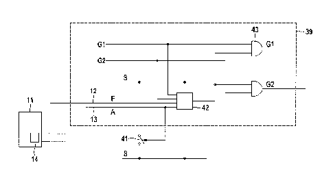
Figure 3 illustrates a monitoring unit 39 of a switching cell 3 and a
monitoring device 11,
which may be arranged in the central control unit 10, in more detail. The
monitoring device
11 has a communication link to the monitoring units 39 of a plurality of
switching cells 3,
preferably to the monitoring units 39 of each of the switching cells 3, and is
able to obtain a
fault signal via a fault signal channel 12 and to transmit a triggering
signal, via a triggering
signal channel 13, to the triggering element 41 of the monitoring unit 40 of
an addressed
switching cell 3 in order to trigger the triggering element 41 and to short-
circuit the switching
cell connections S of the relevant switching cell 3.
The fault signal and the triggering signal may be transmitted, together with a
multiplicity of
other control and notification signals, via an electrical or optical digital
communication link.
The monitoring unit 39 has a voltage detection unit 42 which monitors the
voltage on the
output lines of the switching cell 3. The voltage detection unit 42 outputs a
logic "1" to first
connections of AND gates 43 which are provided for each of the control signals
Cl, G2. The
control signals Cl, G2 for driving the power semiconductor switches 32, 36 are
applied by
the control unit 10 to second connections of the AND gates 43. The voltage
detection unit 42
also receives the control signals G1, G2 from the control unit 10 and masks
voltage
detection, with the result that voltage detection is prevented within a
switching time window
during which the IGBTs are switched. During the periods of time during which
the power
semiconductor switches 32, 36 within the relevant switching cell 3 are not
switched or are in
a switching time window, the voltage detection unit 42 identifies a change in
the voltage
which has occurred, for example, on account of a fault either inside the
relevant switching
cell 3 or on account of an external fault cause.
CA 02794880 2012-11-06
- 12 -
If a voltage change, in particular a voltage change which exceeds a
predetermined voltage
change magnitude, is determined outside the switching time window of the power
semiconductor switches 32, 36, the voltage detection unit 42 generates a logic
"0" which is
respectively applied to the first inputs of the AND gates 43. As a result, the
control signals
G1, G2 are blocked and a logic "0" is applied to the power semiconductor
switches 32, 36 of
the relevant switching cell 3, as a result of which the latter is
disconnected, that is to say
switched off.
At the same time, a fault signal is transmitted to the central monitoring
device 11 via the fault
signal channel 12. With the reception of the first fault signal F, a timer 14
is started in said
monitoring device and monitoring is carried out in order to determine whether
a further fault
signal F is received from a further switching cell 3 during a predetermined
period of time. If a
further fault signal F is received from a further one of the switching cells
3, an external fault is
inferred and the control unit 10 is instructed to change the converter 1 to a
safe state, in
particular by switching off all power semiconductor switches 32, 36 in the
switching cells 3 by
providing suitable control signals G1, G2. In this case, no triggering signal
A which indicates
that the triggering element 41 is intended to be triggered is transmitted.
If a further fault signal is not received from one of the other switching
cells 3 during the
predetermined period of time after the fault signal F was received for the
first time, it can be
assumed that the switching cell 3 whose monitoring unit 39 transmitted the
fault signal F has
a malfunction, and the triggering signal A is transmitted to the triggering
unit 41 of the
relevant switching cell 3, which signal short-circuits the switching cell
connections S of the
relevant switching cell 3.
If a fault signal is instead received from one of the other switching cells 3
during the
predetermined period of time after the fault signal F was received for the
first time, it can be
assumed that the malfunction is outside the switching cell 3 which transmitted
the first fault
signal. In this case, as a response, the power semiconductor switches 32, 36
of the switching
cell 3 which transmitted the first fault signal, of a plurality of the
switching cells 3 or of all
switching cells 3 may be switched off.
According to an alternative embodiment, after the fault signal F has been
received from one
of the switching cells for the first time without a further fault signal being
received within the
CA 02794880 2012-11-06
- 13 -
predetermined period of time, provision may be made for the voltage detection
unit 42 to first
of all be reset via a suitable communication link (not shown), with the result
that the control
signals Cl, G2 are applied to the power semiconductor switches 32, 36 of the
relevant
switching cell 3 again in order to thus reset the switching cell 3 to normal
operation again.
This makes it possible to avoid brief interference, which occurs only once or
a few times,
resulting in complete disconnection of the relevant switching cell 3. The
triggering signal A
can be transmitted to the triggering element 41 of the relevant switching cell
3 only when the
one-off fault in the switching cell 3, which generated the fault signal F, has
been determined
again or a predetermined number of times by the monitoring unit 39 of the
relevant switching
cell 3.
CA 02794880 2012-11-06
- 14 -
List of reference symbols
1 Converter
2 Converter branch
3 Switching cell
4 Induction coil
Control unit
11 Central monitoring device
12 Fault signal channel
13 Triggering signal channel
32, 36 Power semiconductor switches
33, 37 Freewheeling diodes
34, 38 Energy stores
39 Monitoring unit
41 Triggering unit
42 Voltage detection unit
43 AND gate