Note: Descriptions are shown in the official language in which they were submitted.
CA 02795170 2014-07-16
= .
- -
METHOD OF STRIKING A LAMP IN AN ELEC IRONIC DIMILVIING BALLAST CIRCUIT
BACKGROUND OF THE INVENTION
Cross-Reference to Related Applications
[0001] This application is a non-provisional application of
commonly-assigned U.S. Provisional
Application Serial No. 61/321,289, filed April 6, 2010, entitled METHOD OF
STRIKING A LAMP IN
AN ELECTRONIC DIMMING BALLAST.
Field of the Invention
[0002] The present invention relates to electronic ballasts for
controlling a gas discharge lamp,
such as a fluorescent lamp, and more specifically, to a method of striking the
gas discharge lamp.
Description of the Related Art
[0003] In order to reduce energy consumption of artificial
illumination sources, the use of high-
efficiency light sources is increasing, while the use of low-efficiency light
sources (i.e. incandescent
lamps, halogen lamps, and other low-efficacy light sources) is decreasing.
High-efficiency light sources
may comprise, for example, gas discharge lamps (such as compact fluorescent
lamps), phosphor-based
lamps, high-intensity discharge (HID) lamps, light-emitting diode: (LED) light
sources, and other types
of high-efficacy light sources. Since incandescent lamps (including halogen
lamps) generate a continuous
spectrum of light, objects illuminated by incandescent lamps appear as they
would in sunlight thus
providing more pleas ing and accurate color rendering information to the human
eye. Unfortunately,
continuous-spectrum light sources, such as incandescent and halogen lamps,
tend to be very
inefficient.
[0004] In contrast, a much greater percentage of the radiant energy
of fluorescent lamps is
produced inside the visible spectrum than the radiant energy produced by
incandescent lamps. However, a
typical high-efficiency light source does not typically provide a continuous
spectrum of light output, but
rather provides a discrete spectrum of light output. Most of the light
produced by a discrete spectrum light
source is concentrated primarily around one or more discrete wavelengths.
Objects viewed under a
discrete-spectrum light source may not exhibit the full range of colors that
be seen if viewed under a
continuous-spectrum light source.
CA 02795170 2014-07-16
- 2 -
[0005] Lighting control devices, such as dimmer switches, allow for the
control of the amount of
power delivered from a power source to a lighting load, such that the
intensity of the lighting load may be
dimmed. Both high-efficiency and low-efficiency light sources can be dimmed,
but the dimming
characteristics of these two types of light sources typically differ. A low-
efficiency light source can
usually be dimmed to very low light output levels, typically below 1% of the
maximum light output.
However, a high-efficiency light source cannot be typically dimmed to very low
output levels. Low-
efficiency light sources and high-efficiency light sources typically provide
different correlated color
temperatures and color rendering indexes as the light sources are dimmed. The
color of the light output of
a low-efficiency light source (such as an incandescent lamp or a halogen lamp)
typically shifts more
towards the red portion of the color spectrum when the low-efficiency light
source is dimmed to a low
light intensity. In contrast, the color of the light output of a high-
efficiency light source (such as a
compact fluorescent lamp or an LED light source} is normally relatively
constant through its dimming
range with a slightly blue color shift and thus tends to be perceived as a
cooler effect to the eye.
[0006] Generally people have grown accustomed to the dimming performance
and operation of
low-efficiency light sources. As more people begin using high-efficiency light
sources --typically to save
energy -- they are somewhat dissatisfied with the overall performance of the
high-efficiency light sources.
Thus, there has been a long-felt need for a light source that combines the
advantages while minimizing the
disadvantages, of both low-efficiency (i.e., continuous-spectrum) and high-
efficiency (i.e., discrete-
spectrum) light sources. It would be desirable to provide a hybrid light
source that includes a high-
efficiency lamp for saving energy when the light source is controlled to a
high light intensity and a low-
efficiency lamp for providing a pleasing color when the light source is
controlling to a low light intensity.
Thus, there is a need for a method of controlling both lamps of such a hybrid
light source in order to
provide a continuous total light intensity and a pleasing light color across
the dimming range.
SUMMARY OF THE INVENTION
[0007] According to an embodiment of the present invention, a method of
striking a gas
discharge lamp comprises the steps of: (1) generating a high-frequency square-
wave voltage having an
operating frequency; (2) generating a sinusoidal voltage from the high-
frequency square-wave voltage;
(3) coupling the sinusoidal = voltage to the lamp; (4) controlling the
amplitude of the sinusoidal voltage to
a low-end amplitude; and (5) periodically increasing the amplitude of the
sinusoidal voltage during
successive pulse times and then decreasing the amplitude of the sinusoidal
voltage towards the low-end
amplitude at the end of each of the successive pulse times until the lamp has
struck, where the length of
CA 02795170 2014-07-16
- 3 -
each of the successive pulse times is greater than the length of the previous
pulse time. Further, a
maximum amplitude of the sinusoidal voltage during each pulse time may be
greater than a maximum
amplitude of the sinusoidal voltage during the previous pulse time.
[0008] In addition, an electronic ballast for driving a gas discharge
lamp is described herein.
The ballast comprises an inverter circuit for receiving a DC bus voltage and
for generating a high-
frequency square-wave voltage having an operating frequency, a resonant tank
circuit for receiving the
high-frequency square-wave voltage and generating a sinusoidal voltage for
driving the lamp, and a
control circuit coupled to the inverter circuit for controlling the operating
frequency of the high-
frequency AC voltage. The control circuit causes the lamp to strike by
controlling the amplitude of the
sinusoidal voltage to a low-end amplitude, and then periodically increasing
the amplitude of the
sinusoidal voltage during successive pulse times and then decreasing the
amplitude of the sinusoidal
voltage towards the low-end amplitude at the end of each of the successive
pulse times until the lamp has
struck, where the length of each of the successive pulse times being greater
than the length of the
previous pulse time.
[0009] According to another embodiment of the present invention, a hybrid
light source that is
adapted to receive power from an AC power source and to produce a total light
intensity comprises a
continuous-spectrum light source circuit having a continuous-spectrum lamp,
and discrete-spectrum light
source circuit having a gas-discharge lamp. The hybrid light sources controls
the total light intensity
throughout a dimming range from a low-end intensity and high-end intensity.
The discrete-spectrum light
source circuit also comprises an electronic ballast circuit for driving the
gas-discharge lamp. The ballast
circuit has an inverter circuit for generating a high-frequency square-wave
voltage having an operating
frequency, and a resonant tank circuit for receiving the high-frequency square-
wave voltage and
generating a sinusoidal voltage for driving the lamp. The hybrid light source
further comprises a control
circuit coupled to both the continuous-spectrum light source circuit and the
discrete-spectrum light source
circuit for individually controlling the amount of power delivered to each of
the continuous-spectrum
lamp and the gas-discharge lamp, such that the total light intensity of the
hybrid light source is controlled
to a target intensity. The control circuit turns off the gas-discharge lamp
and controls only the continuous-
spectrum lamp to be illuminated when the target intensity is below the
transition intensity. The control
circuit illuminates both the continuous-spectrum lamp and the gas-discharge
lamp when the target
intensity is above the transition intensity. When the target intensity
transitions from below to above the
transition intensity, the control circuit causes the gas-discharge lamp to
strike by controlling the amplitude
of the sinusoidal voltage to a low-end amplitude, and then periodically
increasing the amplitude of the
CA 02795170 2014-07-16
- 4 -
sinusoidal voltage during successive pulse times and then decreasing the
amplitude of the sinusoidal
voltage towards the low-end amplitude at the end of each of the successive
pulse times until the lamp has
struck, where the length of each of the successive pulse times being greater
than the length of the
previous pulse time.
[0010] Other features and advantages of the present invention will become
apparent from the
following description of the invention that refers to the accompanying
drawings.
BRIEF DESCRIPTION OF THE DRAWINGS
[0011] The invention will now be described in greater detail in the
following detailed description
with reference to the drawings in which:
[0012] Fig. 1 is a simplified block diagram of a lighting control system
including a hybrid light
source and a dimmer having a power supply according to an embodiment of the
present invention;
[0013] Fig. 2 is a simplified side view of the hybrid light source of
Fig. 1;
[0014] Fig, 3 is a simplified top cross-sectional view of the hybrid
light source of Fig. 2;
[0015] Fig. 4A is a simplified graph showing a total correlated color
temperature of the hybrid
light source of Fig. 2 plotted with respect to a desired total lighting
intensity of the hybrid light source;
[0016] Fig. 4B is a simplified graph showing a target fluorescent lamp
lighting intensity, a target
halogen lamp lighting intensity, and a total lighting intensity of the hybrid
light source of Fig. 2 plotted
with respect to the desired total lighting intensity;
[0017] Fig. 5 is a simplified block diagram of the hybrid light source of
Fig. 2;
[0018] Fig. 6 is a simplified schematic diagram showing a portion of the
hybrid light source of
Fig. 2 according to a first embodiment of the present invention;
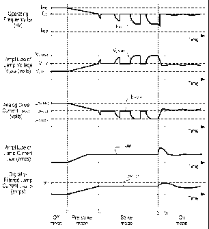
[0019] Fig. 7 shows example waveforms that illustrate the operation of
the hybrid light source of
Fig. 2;
[0020] Figs. 8A and 8B are simplified flowcharts of a fluorescent lamp
control procedure
executed periodically by a microprocessor of the hybrid light source of Fig. 6
according to the first
CA 02795170 2014-07-16 =
- 5 -
embodiment of the present invention;
[0021] Fig. 9 is n simplified schematic diagram showing a portion of a
hybrid light source according
to a second embodiment of the present invention;
[0022] Fig. 10 shows example waveforms that illustrate the operation of
the hybrid light source
of Fig. 9; and
[0023] Figs. 11A and 11B are simplified flowcharts of a fluorescent lamp
control procedure
executed periodically by a microprocessor of the hybrid light source of Fig. 9
according to the first
embodiment of the present invention.
DETAILED DESCRIPTION OF THE INVENTION
[0024] The foregoing summary, as well as the following detailed
description of the preferred
embodiments, is better understood when read in conjunction with the appended
drawings. For the
purposes of illustrating the invention, there is shown in the drawings an
embodiment that is presently
preferred, in which like numerals represent similar parts throughout the
several views of the drawings, it
being understood, however that the invention is not limited to the specific
method and instrumentalities
disclosed.
[0025] Fig. 1 is a simplified block diagram of lighting control system 10
including a hybrid
light source 100 according to an embodiment of the present invention. The
hybrid light source 100 is
coupled to the hot side of an alternating-current (AC) power source 102 (e.g.,
120 VAC, 60 Hz) through a
conventional two-wire dimmer switch 104 and is directly coupled to the neutral
side of the AC power
source. The dimmer switch 104 comprises a user interface 105A including an
intensity adjustment
actuator (not shown), such as a slider control or a rocker switch. The user
interface 105A allows a user to
adjust a desired total lighting intensity LDESIRED of the hybrid light source
100 across a dimming range
between a low-end lighting intensity LLE (i.e., a minimum intensity, e.g., 0%)
and a high-end lighting
intensity LHE (i.e., a maximum intensity, e.g., 100%).
[0026] The dimmer switch 104 typically includes a bidirectional
semiconductor switch 105B,
such as, for example, a thyristor (such as a triac) or two field-effect
transistors (FETs) coupled in anti-
series connection, for providing a phase-controlled voltage Vpc (i.e., a
dimmed-hot voltage) to the hybrid
light source 100. Using a standard forward phase-control dimming technique, a
control circuit 105C
CA 02795170 2014-07-16
= =
- 6 -
renders the bidirectional semiconductor switch 105B conductive at a specific
time each half-cycle of the
AC power source, such that the bidirectional semiconductor switch remains
conductive for a conduction
period TcoN during each half-cycle. The dimmer switch 104 controls the amount
of power delivered to the
hybrid light source 100 by controlling the length of the conduction period
Tc0N. The dimmer switch 104
also often comprises a power supply 105D coupled across the bidirectional
semiconductor switch 105B
for powering the control circuit 105C. The power supply 105D generates a DC
supply voltage Vps by
drawing a charging current IcHRG from the AC power source 102 through the
hybrid light source 100
when the bidirectional semiconductor switch 105B is non-conductive each half-
cycle. An example of a
dimmer switch having a power supply 105D is described in greater detail in
U.S. Patent No. 5,248,919,
issued September 29, 1993, entitled LIGHTING CONTROL DEVICE.
[0027] Alternatively, the dimmer switch 104 could comprise a two-wire
analog dimmer switch
having a timing circuit (not shown) and a trigger circuit (not shown). The
timing circuit conducts a timing
current from the AC power source through the hybrid light source 100 when the
bidirectional
semiconductor switch 105B is non-conductive each half-cycle. The timing
current is used to control when
the bidirectional semiconductor switchl 05B is rendered conductive each half-
cycle.
[0028] Fig. 2 is a simplified side view and Fig. 3 is a simplified top
cross-sectional view of the
hybrid light source 100. The hybrid light source 100 comprises both a discrete-
spectrum lamp and a
continuous-spectrum lamp. The discrete-spectrum lamp may comprise, for
example, a gas discharge
lamp, such as, a compact fluorescent lamp 106. The compact fluorescent lamp
106 may comprise, for
example, three curved gas-filled glass tubes 109 as shown in Fig. 2. The
continuous-spectrum lamp may
comprise, for example, an incandescent lamp (such as halogen lamp 108) or any
suitable low-efficiency
lamp having a continuous spectrum. For example, the halogen lamp 108 may
comprise a low-voltage
halogen lamp that may be energized by a voltage having a magnitude ranging
from approximately 12
volts to 24 volts. Alternatively, the halogen lamp108 may comprise a line-
voltage halogen lamp (e.g.,
energized by an AC voltage having an amplitude of approximately 120 VAC). The
discrete-spectrum lamp
(i.e., the fluorescent lamp 106) may have a greater efficacy than the
continuous-spectrum lamp (i.e., the
halogen lamp 108). For example, the fluorescent lamp 106 may be typically
characterized by an efficacy
greater than the approximately 60 lm/W, while the halogen lamp 108 may be
typically characterized by
an efficacy less than approximately 30 lm/W.
[0029] The hybrid light source 100 comprises, for example, a screw-in
Edison base 110 for
connection to a standard Edison socket, such that the hybrid light source may
be coupled to the AC
CA 02795170 2014-07-16
- 7 -
power source 102. The screw-in base 110 has two input terminals 110A, 110B
(Fig. 5) for receipt of the
phase-controlled voltage Vpc and for coupling to the neutral side of the AC
power source 102. A hybrid
light source electrical circuit 120 (Fig. 5) is housed in an enclosure 112 and
controls the amount of power
delivered from the AC power source to each of the fluorescent lamp 106 and the
halogen lamp 108. The
fluorescent lamp 106 and halogen lamp 108 may be surrounded by a housing
comprising a light diffuser
114 (e.g., a glass light diffuser) and a fluorescent lamp reflector 115. The
fluorescent lamp reflector 115
directs the light emitted by the fluorescent lamp 106 away from the hybrid
light source 100. The halogen
lamp 108 is mounted to a post 116, such that the halogen lamp is situated
beyond the terminal end of the
fluorescent lamp 106. The post 116 allows the halogen lamp to be electrically
connected to the hybrid
light source electrical circuit 120. A halogen lamp reflector 118 surrounds
the halogen lamp 108 and
directs the light emitted by the halogen lamp in the same direction as the
fluorescent lamp reflector 115
directs the light emitted by the fluorescent lamp 106.
[0030]
The hybrid light source 100 provides an improved color rendering index and
correlated
color temperature across the dimming range of the hybrid light source
(particularly, near a low-end
lighting intensity LLE) as compared to a stand-alone compact fluorescent lamp.
Fig. 4A is a simplified
graph showing a total correlated color temperature TTOTAL of the hybrid light
source 100 plotted with
respect to the desired total lighting intensity LDES1RED of the hybrid light
source 100 (as determined by the
user actuating the intensity adjustment actuator of the user interface 105A of
the dimmer switch 104). A
correlated color temperature TFL of a stand-alone compact fluorescent lamp
remains constant at
approximately 2700 Kelvin throughout most of the dimming range. A correlated
color temperature THAL
of a stand-alone halogen lamp decreases as the halogen lamp is dimmed to low
intensities causing a
desirable color shift towards the red portion of the color spectrum and
creating a warmer effect on the
human eye.
The hybrid light source 100 is operable to individually control the
intensities of the
fluorescent lamp 106 and the halogen lamp 108, such that the total correlated
color temperature TTOTAL of
the hybrid light source 100 more closely mimics the correlated color
temperature of the halogen lamp at
low light intensities, thus more closely meeting the expectations of a user
accustomed to dimming low-
efficiency lamps.
[0031]
The hybrid light source 100 is further operable to control the fluorescent
lamp 106 and
the halogen lamp 108 to provide high-efficiency operation near the high-end
intensity LHE. Fig. 4B is a
simplified graph showing a target fluorescent lighting intensity LFL, a target
halogen lighting intensity
LHAL, and a target total lighting intensity LTOTAL plotted with respect to the
desired total lighting intensity
LDEsiRED of the hybrid light source 100 (as determined by the user actuating
the intensity adjustment
CA 02795170 2014-07-16
- 8 -
actuator of the dimmer switch 104). The target fluorescent lighting intensity
LEL and the target halogen
lighting intensity LHAL (as shown in Fig. 4B) provide for a decrease in color
temperature near the low-end
intensity LLE and high-efficiency operation near the high-end intensity LHE.
Near the high-end intensity
LHE, the fluorescent lamp 106 (i.e., the high-efficiency lamp) provides a
greater percentage of the total
light intensity LTOTAL of the hybrid light source. As the total light
intensity LTOTAL of the hybrid light
source 100 decreases, the halogen lamp 108 is controlled such that the halogen
lamp begins to provide a
greater percentage of the total light intensity.
[0032] The structure and operation of the hybrid light source 100 is
described in greater detail in
commonly-assigned, co-pending U.S. Patent Application No. 12/205,571, filed
September 8, 2008; U.S.
Patent Application No. 12/553,612, filed September 3, 2009; and U.S. Patent
Application No. 12/704,781,
filed February 12, 2010; each entitled HYBRID LIGHT SOURCE.
[0033] Because the fluorescent lamp 106 cannot be dimmed to very low
intensities without the
use of more expensive and complex circuits, the fluorescent lamp 106 is
controlled to be off at a transition
intensity LTRAN, e.g., approximately 8% (as shown in Fig. 4B) or up to
approximately 30%. Across the
dimming range of the hybrid light source 100, the intensities of the
fluorescent lamp 106 and the halogen
lamp 108 are individually controlled such that the target total light
intensity LTOTAL of the hybrid light
source 100 is substantially linear as shown in Fig. 4B. Below the transition
intensity LTRAN, the halogen
lamp provides all of the total light intensity LTOTAL of the hybrid light
source 100, thus providing for a
lower low-end intensity LLE than can be provided by a stand-alone fluorescent
lamp. Immediately above
the transition intensity LTRAN, the fluorescent lamp 106 is controlled to a
minimum fluorescent intensity
LELNIN. Immediately below the transition intensity LTRAN, the halogen lamp is
108 is controlled to a
maximum halogen intensity LHAL-MAX, which is, for example, approximately 80%
of the maximum rated
intensity of the halogen lamp. When the desired total lighting intensity
LDESIRED of the hybrid light source
100 transitions above the transition intensity LTRAN, the target halogen
lighting intensity LHAL is reduced
below the maximum halogen intensity LHAL-MAX and fluorescent lamp 106 is
controlled to a minimum
fluorescent intensity LFL-MIN (e.g., approximately 5%), such that the total
light intensity LTOTAL is
approximately equal to the maximum halogen intensity LHAL-MAX= Since the
fluorescent lamp 106 is
turned on at the transition intensity LTRAN in the middle of the dimming range
of the hybrid light source
100 as shown in Fig. 4B, the hybrid light source 100 of the present invention
provides a method of
striking the fluorescent lamp 106 to turn the lamp on to low-end (i.e., to the
minimum fluorescent
intensity LELNIN) that avoids flickering, flashing, or brightness overshoot of
the intensity of the lamp as
well be described in greater detail below.
CA 02795170 2014-07-16
- 9 -
[0034] Fig. 5 is a simplified block diagram of the hybrid light source
100 showing the hybrid
light source electrical circuit 120. The hybrid light source 100 comprises a
radio-frequency interference
(RFI) filter 130 coupled across the input terminals 110A, 110B for minimizing
the noise provided to the
AC power source 102. The hybrid light source 100 further comprises a high-
efficiency light source circuit
140 (i.e., a discrete-spectrum light source circuit) for illuminating the
fluorescent lamp 106 and a low-
efficiency light source circuit 150 (i.e., a continuous-spectrum light source
circuit) for illuminating the
halogen lamp 108. A control circuit 160 simultaneously controls the operation
of the high-efficiency light
source circuit 140 and the low-efficiency light source circuit 150 to thus
control the amount of power
delivered to each of the fluorescent lamp 106 and the halogen lamp 108. A
power supply 162 generates a
direct-current (DC) supply voltage Vcc (e.g., 5 VDc) for powering the control
circuit 160.
[0035] The control circuit 160 is operable to determine the desired total
lighting intensity
LDESIRED of the hybrid light source 100 in response to a zero-crossing detect
circuit 164 (i.e., as
determined by the user actuating the intensity adjustment actuator of the user
interface 105A of the
dimmer switch 104). The zero-crossing detect circuit 164 provides a zero-
crossing control signal Vzc,
representative of the zero-crossing of the phase-controlled voltage Vpc, to
the control circuit 160. A zero-
crossing is defined as the time at which the phase-controlled voltage Vpc
changes from having a
magnitude of substantially zero volts to having a magnitude greater than a
predetermined zero-crossing
threshold Vm_zc (and vice versa) each half-cycle. Specifically, the zero-
crossing detect circuit 164
compares the magnitude of the rectified voltageto the predetermined zero-
crossing threshold Vill_zc (e.g.,
approximately 20 V), and drives the zero-crossing control signal Vzc high
(i.e., to a logic high level, such
as, approximately the DC supply voltage Vcc) when the magnitude of the phase-
controlled voltage Vpc is
greater than the predetermined zero-crossing threshold VTH-ZC. Further, the
zero-crossing detect circuit
164 drives the zero-crossing control signal Vzc low (i.e., to a logic low
level, such as, approximately
circuit common) when the magnitude of the phase-controlled voltage Vpc is less
than the predetermined
zero-crossing threshold VTH_zc. The control circuit 160 determines the length
of the conduction period
Tc0N of the phase-controlled voltage Vpc in response to the zero-crossing
control signal Vzc and then
determines the target lighting intensities for both the fluorescent lamp 106
and the halogen lamp 108 to
produce the target total lighting intensity LTOTAL of the hybrid light source
100 in response to the
conduction period Tc0N of the phase-controlled voltage Vpc. Alternatively, the
zero-crossing detect circuit
164 may provide some hysteresis in the level of the zero-crossing threshold
VTH_zc.
[0036] The low-efficiency light source circuit 150 comprises a full-wave
rectifier 152 for
generating a rectified voltage VREcT (from the phase-controlled voltage Vpc)
and a halogen lamp drive
CA 02795170 2014-07-16
. =
- 10 -
circuit 154, which receives the rectified voltage VREcT and controls the
amount of power delivered to the
halogen lamp 108. The low-efficiency light source circuit 150 is coupled
between the rectified voltage
VRECT and the rectifier common connection (i.e., across the output of the
front end circuit 130). The
control circuit 160 is operable to control the intensity of the halogen lamp
108 to the target halogen
lighting intensity LHAL corresponding to the present value of the desired
total lighting intensity LDESIRED of
the hybrid light source 100, e.g., to the target halogen lighting intensity as
shown in Fig. 4B. Since the
halogen lamp 108 is a low-voltage halogen lamp, the halogen drive circuit 154
comprises a low-voltage
transformer (not shown) coupled between the rectifier 152 and the halogen
lamp.
[0037] The high-efficiency light source circuit 140 comprises a
fluorescent drive circuit (e.g., a
dimmable electronic ballast circuit 142) for receiving the phase-controlled
voltage Vpo (via the RFI filter
130) and for driving the fluorescent lamp 106. Specifically, the phase-
controlled voltage Vpc is coupled to
a voltage coupler circuit 144, which generates a bus voltage VBus across two
series connected bus
capacitors CB1, C82. The first bus capacitor CBI is operable to charge through
a diode DI during the
positive half-cycles, which the second bus capacitor CB2 is operable to charge
through a diode D2 during
the negative half-cycles. The ballast circuit 142 includes an inverter circuit
145 for converting the DC bus
voltage VBus to a high-frequency square-wave voltage Vso. The high-frequency
square-wave voltage Vs()
is characterized by an operating frequency fop (and an operating period Top =
140). The ballast circuit
142 further comprises an output circuit. e.g., a resonant tank circuit 146,
for filtering the square-wave
voltage Vso to produce a substantially sinusoidal high-frequency AC voltage
VsiN, which is coupled to the
electrodes of the fluorescent lamp 106. The high-efficiency lamp source
circuit 140 further comprises a
lamp voltage measurement circuit 148 (which provides a lamp voltage control
signal VLAMP_VLT
representative of an amplitude of a lamp voltage VLAmp to the control circuit
160), and a lamp current
measurement circuit 149 (which provides a lamp current control signal VLAMP
CUR representative of an
amplitude of a lamp current 'LAMP to the control circuit).
[0038] The control circuit 160 is operable to control the inverter
circuit 145 of the ballast circuit
140 to control the intensity of the fluorescent lamp 106 to the target
fluorescent lighting intensity LEL
corresponding to the present value of the desired total lighting intensity
LDESIRED of the hybrid light source
100 in response to the zero-crossing control signal Vzc from the zero-crossing
detect circuit 164 (i.e.,
according to the graph show in in Fig. 4B). The control circuit 160 determines
a target lamp current
'TARGET for the fluorescent lamp 106 that corresponds to the target
fluorescent lighting intensity LpL. The
control circuit 160 then controls the operation of the inverter circuit 145 in
response to the lamp voltage
control signal VLAMP_VLT and the lamp current control signal VLAMP_CUR in
order to control the lamp
CA 02795170 2014-07-16
- 11 -
current ILAjvip towards the target
lamp current 'TARGET.
[0039] Fig. 6 is a simplified schematic diagram of the hybrid light
source 100 showing the
inverter circuit 145, the resonant tank 146, and the control circuit 160 of
the hybrid light source electrical
circuit 120 in greater detail according to a first embodiment of the present
invention. Fig. 7 shows
example waveforms that illustrate the operation of the hybrid light source
electrical circuit 120. The
inverter circuit 145 comprises first and second semiconductor switches, e.g.,
field-effect transistors
(FETs) Q210, Q212, and a gate drive circuit 214, which is coupled to control
inputs (i.e., gates) of the
FETs for rendering the FETs conductive and non-conductive in order to generate
the high-frequency
square-wave voltage VsQ at the output of the inverter circuit. The gate drive
circuit 214 controls the FETs
Q210, Q212 in response to an oscillator circuit 216, which sets the operating
frequency fop of the high-
frequency square-wave voltage VsQ. The control circuit 160 controls the
oscillator circuit 216 to adjust the
operating frequency fop of the high-frequency square-wave voltage VsQ as will
be described in greater
detail below.
[0040] The high-frequency square-wave voltage Vs() is provided to the
resonant tank circuit 146,
which includes a resonant inductor L220 and a resonant capacitor C222. The
resonant inductor L220 and
the resonant capacitor C222 operate to filter the high-frequency square-wave
voltage VsQ to produce the
substantially sinusoidal voltage VsIN for driving the fluorescent lamp 106.
The amplitude of the sinusoidal
voltage VsIN is dependent upon the operating frequency fop of the high-
frequency square-wave voltage
VsQ. The resonant tank circuit 146 is characterized by a resonant frequency
fREs, which is defined by the
values of the resonant inductor L220 and the resonant capacitor C222. The
sinusoidal voltage VSIN is
coupled to the fluorescent lamp 106 through a DC-blocking capacitor C224,
which prevents any DC
characteristics of the inverter circuit 145 from being coupled to the
fluorescent lamp 106. The resonant
inductor 220 is magnetically coupled to two filament windings 226, which are
electrically coupled to the
filaments of the fluorescent lamp 106. The power supply 162 (Fig. 5) may draw
current from an
additional winding (not shown) that is magnetically coupled to the resonant
inductor 220.
[0041] Before the fluorescent lamp 106 is turned on (i.e., struck), the
filaments of the lamp must
be heated in order to extend the life of the lamp. Particularly, whenever the
fluorescent lamp 106 of the
hybrid light source 100 of the present invention is not illuminated, the
operating frequency fop of the
inverter circuit 145 is controlled to a preheat frequency fpRE (as shown in
Fig. 7), such that the amplitude
of the voltage generated across the first and second windings of the resonant
inductor L220 increases, and
CA 02795170 2014-07-16
- 12 -
the filament windings 226 provide filament voltages to the .filaments of the
fluorescent lamp 106 for
heating the filaments.
[0042] The control circuit 160 comprises, for example, a microprocessor
230 for managing the
operation of the FETs Q210, Q212 of the inverter circuit 145. The
microprocessor 230 may alternatively
be implemented as a programmable logic device (PLD), a microcontroller, an
application specific
integrated circuit (ASIC), or any other suitable processing device or control
circuit. The microprocessor
230 generates a target control signal VTARGET, which comprises, for example, a
DC voltage having a
magnitude representative of the target fluorescent lighting intensity LFL of
the fluorescent lamp 106. The
control circuit 160 also includes a proportional-integral (PI) controller 232,
which attempts to minimize
the error between target control signal VTARGET and the lamp current control
signal VLAMP CUR (i.e., the
difference between the target lamp current 'TARGET for the fluorescent lamp
106 and the present amplitude
of the lamp current ILAmp). The PI controller 232 has an output for generating
an output control signal Vpi,
which is representative of the operating frequency fop required to control the
lamp current 'LAMP to be
equal to the target lamp current 'TARGET.
100431 The control circuit 160 further comprises a strike control circuit
234, which controls the
operating frequency fop of the inverter circuit 145 during striking of the
fluorescent lamp 106.
Specifically, the strike control circuit 234 receives a strike control signal
VsTK from the microprocessor
230 and provides a strike override control signal VsncovR to the oscillator
circuit 216 of the inverter
circuit 145, such that the oscillator circuit adjusts the operating frequency
fop of the inverter circuit 145 in
response to the strike override control signal Vsrx-ovR. The strike control
circuit 234 also receives the
lamp voltage control signal VLAMP_VLT from the lamp voltage measurement
circuit 148 and regulates the
magnitude of the strike override control signal VsncovR so as to limit the
amplitude of the lamp voltage
VLAMP to a maximum lamp voltage VLTAA); (as shown in Fig. 7).
[00441 The control circuit 160 further comprises a clamp circuit 236,
which is controlled in
response to a clamp enable control signal VcLAmp_EN and a clamp level control
signal VCLAMP-LVL that are
generated by the microprocessor 230. The clamp circuit 236 operates to clamp
the output of the PI
controller 232 (i.e., the output control signal Vp1) when the clamp enable
control signal VcrAmp_EN is
driven high (i.e., to approximately the supply voltage Vcc). When the clamp
level control signal VÃTAmp_
LvL is driven high to, for example, approximately the supply voltage Vcc, the
output control signal Vp1 of
the PI controller 232 is clamped to a pre-heat control voltage Vpi_pRE, which
causes the operating
frequency fop of the inverter circuit 145 to be controlled to the preheat
frequency fpRE for pre-heating the
CA 02795170 2014-07-16
. =
- 13 -
filaments of the lamp 106. The microprocessor 230 is operable to decrease the
clamp level control signal
VcLAMP-LVL below the supply voltage Vcc prior to attempting to strike the
fluorescent lamp 106.
[0045] According to the present invention, the control circuit 160
attempts to strike the
fluorescent lamp 106 by periodically "blipping" the operating frequency fop of
the inverter circuit 145
down towards the resonant frequency fREs to control the amplitude of the lamp
voltage VLAmp as shown in
Fig. 7. The plot of the amplitude of the lamp voltage VLAMp shown in Fig. 7
represents the envelope of the
actual high-frequency lamp voltage VLAmp. When a lamp strike is requested
(i.e., when the desired total
lighting intensity LDESIRED is increased above the transition intensity
LTRAN), the microprocessor 130 first
controls the operating frequency fop to a low-end frequency fLE and then
increases the amplitude of the
lamp voltage VLAmp during successive pulse times (e.g., Tp1, Tp2, Tp3 shown in
Fig. 7), where the length of
each of the successive pulse times is greater than the length of the precious
pulse time (i.e., the
successive pulse times have increasing lengths, such that Tp3> Tp2 > Tp1).
During each of the successive
pulse times, the amplitude of the lamp voltage \lump increases with respect to
time (e.g., exponentially) to
a maximum amplitude VmA across the length of the pulse time. The maximum
amplitude VmA of the
sinusoidal lamp voltage VLAmp during each successive pulse time may be greater
than the maximum
amplitude VmA of the sinusoidal lamp voltage VLAmp during the previous pulse
time, i.e., the maximum
amplitude VmA of the sinusoidal lamp voltage VLAmp during the second pulse
time Tp2 is greater than the
maximum amplitude Vivi!, during the first pulse time Tp1 In addition, the
amplitude of the lamp voltage
VLAmp is limited to the maximum lamp voltage VL_mAx by the strike control
circuit 234. Alternatively, the
amplitude of the lamp voltage VLAmp could be increased to a constant amplitude
(e.g., to the maximum
lamp voltage VL_max) during each of the successive pulse times, such that the
maximum amplitudes VmA of
the sinusoidal lamp voltage VLAmp during each of the successive pulse times
are equal.
[0046] When the fluorescent lamp 106 is off (i.e., during an off mode),
the microprocessor 230
drives the clamp enable control signal VCLAMP-EN high and adjusts the
magnitude of the clamp level
control signal VaAmp_LvL, such that the clamp circuit 236 controls the
operating frequency fop of the
inverter circuit 145 to preheat frequency fpRE (as shown in Fig. 7). Since the
operating frequency fop is
maintained at the preheat frequency fpRE when the fluorescent lamp 106 is off,
the filaments will be heated
appropriately when the fluorescent lamp is turned on in response to a change
in the desired total lighting
intensity LDESIRED that transitions above the transition intensity LTRAN
(e.g., in response to an actuation of
the intensity adjustment actuator of the dimmer switch 104). When a
fluorescent lamp strike is requested
(i.e., when the desired total lighting intensity LDESIRED is increased above
the transition intensity LTRAN),
the operating frequency fop of the inverter circuit 145 is controlled such
that the amplitude of the voltage
CA 02795170 2014-07-16
- 14 -
across the resonant capacitor C222 increases until the fluorescent lamp 106
strikes and the lamp current
LAMP begins to flow through the lamp as will be desired in greater detail
below.
[0047] When the desired total lighting intensity LDESIRED of the hybrid
light source 100 is
increase above the transition intensity LTRAN at time tt in Fig. 7), the
microprocessor 230
will attempt to strike the fluorescent lamp 106 to thus turn the lamp on.
Before striking the fluorescent
lamp 106 (i.e., during a pre-strike mode), the microprocessor 230 decreases
the magnitude of the clamp
level control signal VCLAMP-LVL with respect to time until the lamp voltage
VLAmp rises to a low-end lamp
amplitude VL_LE and the operating frequency fop drops to the low-end frequency
fEE (e.g., at time t2 in Fig.
7).
[0048] At this time, the microprocessor 230 attempts to strike the
fluorescent lamp 106 to thus
illuminate the lamp (i.e., during a strike mode). Specifically, the
microprocessor 230 drives the strike
control signal VsTK high in successive pulses of increasing length to
periodically adjust the operating
frequency fop of the inverter circuit 145 down towards the resonant frequency
fREs as shown in Fig. 7 to
try to strike the lamp 106. During each successive pulse time, the operating
frequency fop is decreased
below the low-end frequency fix, such that the amplitude of the lamp voltage
VLAmp increases above the
low-end lamp amplitude Vy_LE. As previously mentioned, the length of each of
the successive pulses is
greater than the length of the previous pulse. At the beginning of each pulse
time, the microprocessor 230
drives the strike control signal VsTK high to approximately the supply voltage
Vcc and the strike control
circuit 234 increases the magnitude of the strike override control signal VSTK-
OVR with respect to time at a
predetermined rate across the length of the pulse time (e.g., at an
exponential rate as shown in Fig. 7). In
response to the magnitude of the strike override control signal VSTK-OVR, the
oscillator circuit 216
decreases the operating frequency fop of the inverter circuit 145 below the
low-end frequency
frE at a
similar rate.
[0049] The magnitude of the strike override control signal Vs-rx-ovR is
regulated by the strike
control circuit 234 so as to limit the lamp voltage VLAmp to the maximum lamp
voltage VL-MAx. When the
strike control signal VsTK is driven low (i.e., to approximately circuit
common), the strike control circuit
234 immediately drives the strike override control signal VSTK-OVR low to thus
bring the operating
frequency fop back to the low-end frequency fLE set by the clamp circuit 236.
For example, the first pulse
time Tp1 during the strike mode may have a minimum length TmiN, e.g.,
approximately 500 usec. Each
subsequent successive pulse time (e.g., Tp2 and Tp3) may have a length that is
predetermined increment
TDELTA (e.g., approximately 50 usec) longer than previous pulse (e.g., Tp2=-
Tpi+Tdelia and Tp3=TP2+
CA 02795170 2014-07-16
- 15 -
TDELTA)= In addition, a strike attempt period TsTK between the beginnings of
the pulses may be constant
(e.g., approximately 1.5 msec) as shown in Fig. 7. Accordingly, the control
circuit 160 controls the
inverter circuit 145 in the strike mode so as to increase the amplitude of the
lamp voltage VLAMP during
successive pulse times, where the successive pulse times having increasing
lengths and may have
increasing maximum amplitudes as shown in Fig. 7.
[0050] The microprocessor 230 is operable to determine when the
fluorescent lamp 106 has
struck in response to the amplitude of the lamp current 'LAMP. The
microprocessor 230 digitally filters the
amplitude of the lamp current 'LAMP (i.e., from the lamp current control
signal VLAMP_CUR) to generate a
digitally-filtered lamp current ILAmp_DF as shown in Fig. 7. In addition, the
lamp current control signal
VLAMP_CUR may be also filtered by an analog filter circuit. The microprocessor
230 determines that the
fluorescent lamp 106 has struck when the magnitude of the digitally-filtered
lamp current ILATAP_DF rises to
a strike current threshold IsTK. When the fluorescent lamp 106 strikes (e.g.,
at time t3 in Fig. 7), the
amplitude of the lamp current 'LAMP increases quickly. The magnitude of the
digitally-filtered lamp
current 'LAMP-Dp also increases, but at a slower rate than the amplitude of
the lamp current 'LAMP.
Therefore, the microprocessor 230 is operable to detect that the fluorescent
lamp 106 has struck a short
period of time (e.g., at time t4 in Fig. 7) after the lamp actually struck as
shown in Fig. 7.
[0051] The "dead times" between the pulse times of the strike control
signal VsTK (i.e., when the
strike control signal VsTK is equal to approximately zero volts) help reduce
overshoot of the lamp current
'LAMP that may be caused by the delay between when the fluorescent lamp 106
strikes and when the
digitally-filtered lamp current ILAmp_DF rises to the strike current threshold
Ism. Overshoot of the lamp
current 'LAMP can cause visible flicking, flashing, or brightness overshoot of
the intensity of the
fluorescent lamp 106. Striking of a fluorescent lamp 106 is dependent the
amplitude of the lamp voltage
VLAMP and the length of time that the lamp voltage VLAMP having that amplitude
is coupled across the
lamp. Since these parameters may vary from one lamp to another or between
different lamp types,
different lamps may require different numbers of successive pulse times of the
lamp voltage VLAMP in
order to strike. Because the amplitude of the lamp voltage VLAMP is only
increased during the successive
pulse times and is controlled back to approximately the low-end lamp amplitude
VL_LE during the dead
times of the strike control signal VsTK, the electronic ballast circuit 142 is
able to accommodate striking
different lamps having different operating characteristics while minimizing
the overshoot of the lamp
current 'LAMP.
[0052] When the microprocessor 230 detects that the fluorescent lamp 106
has struck, the
CA 02795170 2014-07-16
- =
- 16 -
microprocessor drives the clamp enable control signal VcLAmp_EN 10W, such that
the clamp circuit 236 no
longer clamps the output control signal Vp1 of the PI controller 232. Thus,
the operating frequency fop of
the inverter circuit 145 is then controlled in response to the output control
signal Vpi of the PI controller
232 to drive the lamp current 'LAMP to be equal to the target lamp current
'TARGET (i.e., during an on mode).
Because of the delay between when the fluorescent lamp 106 strikes and when
the digitally-filtered lamp
current ILAstip_DF rises to the strike current threshold IsTR, the
microprocessor 230 typically detects that the
lamp has struck during the dead times of the strike control signal VsTK. Since
the amplitude of the lamp
voltage VLAmp is controlled back to approximately the low-end lamp amplitude
VL_TE during the dead time
the lamp 106 will be turned on to approximately the minimum fluorescent
intensity LEL-MIN and overshoot
of the lamp current ITAN4p is minimized.
[0053] Figs. 8A and 8B are simplified flowcharts of a fluorescent lamp
control procedure 300
executed periodically (e.g., approximately every 100 usec) by the
microprocessor 230 of the control
circuit 160 according to the first embodiment of the present invention. If the
microprocessor 230 is
operating in the on mode at step 310 (i.e., if the fluorescent lamp 106 is
illuminated), but there is presently
no change in the desired total lighting intensity LDESIRED of the hybrid light
source 100 (as determined
from the zero-crossing control signal Vzc received from the zero-crossing
detect circuit 164) at step 312,
the fluorescent lamp control procedure 300 simply exits. If there has been a
change in the desired total
lighting intensity LDESIRED at step 312, but the change does not take the
desired total lighting intensity
LDESIRED below the transition intensity LTRAN (i.e., the fluorescent lamp 106
should stay on) at step 314,
the microprocessor 230 adjusts the target control signal VTARGET appropriately
in response to the change in
the desired total lighting intensity LDESIRED at step 316. However, if the
change takes the desired total
lighting intensity LDESIRED below the transition intensity LTRAN at step 314,
the microprocessor 230
changes to the off mode at step 318 and drives the clamp enable control signal
VCLAMP-EN high to
approximately the supply voltage Vcc at step 320. The microprocessor 230 also
drives the clamp level
control signal VCLAMP-LVL high to approximately the supply voltage Vcc (to
control the operating
frequency fop of the inverter circuit 145 to the preheat frequency fpRE) at
step 322, before the fluorescent
lamp control procedure 300 exits.
[0054] If the microprocessor 230 is operating in the off mode (i.e., the
fluorescent lamp 106 is
off) at step 234 and the microprocessor has received a command to transition
the desired total lighting
intensity LDESIRED of the hybrid light source 100 above the transition
intensity LTRAN at step 326, the
microprocessor 230 changes to the pre-strike mode at step 328, before the
fluorescent lamp control
procedure 300 exits. If the microprocessor 230 is not operating in the off
mode at step 324, but is
CA 02795170 2014-07-16
. .
- 17 -
operating in the pre-strike mode at step 330, the microprocessor 230 decreases
the magnitude of the clamp
level control signal VCLAmp_LvL by a predetermined value VCLAMP-DELTA at step
332, such that the operating
frequency fop will decrease and the lamp voltage VLAMp will increase. As the
microprocessor 230
continues to periodically execute the fluorescent lamp control procedure 300
while in the pre-strike mode,
the microprocessor will continue to decrease the magnitude of the clamp level
signal VCLAMP-LVL by the
predetermined value VcLAmp_DELTA at step 332. When the amplitude of the lamp
voltage VLAAmp (as
determined from the lamp voltage control signal VLAMP_VLT) is greater than or
equal to the low-end lamp
amplitude VL_LE at step 334, the microprocessor 230 changes to the strike mode
at step 336 (during which
the microprocessor will maintain the magnitude of the clamp level control
signal VCLAMP-LVL constant) and
sets a variable n equal to zero at step 338, before the fluorescent lamp
control procedure 300 exits. The
microprocessor 230 uses the variable n to count the number of pulses of the
strike control signal VsTK
during the strike mode.
[0055] Referring to Fig. 8B, if the microprocessor 230 is operating in
the strike mode at step 340
and the magnitude of the digitally-filtered lamp current ITAmp_Dp is less than
the strike current threshold
Isix at step 342, the microprocessor 230 operates to generate the strike
control signal VsTK with the
successive pulse having increasing pulse lengths, so as to increase the
amplitude of the lamp voltage
VTAmp during the successive pulse times. The microprocessor 230 uses a pulse
timer to determine when to
start and end each of the pulse times of the strike control signal VsTK. For
example, the pulse timer may
decrease in value with respect to time, and the microprocessor 230 may
initialize the pulse timer with the
strike attempt period TsK, such that microprocessor will begin to generate
another pulse when the pulse
timer is equal to or less than approximately zero. Specifically, if the
microprocessor 230 should begin to
generate a new pulse at step 344, the microprocessor determines a length
TpuTsE of the next pulse time at
step 346, i.e.,
TPLILSE TMN MTdeLta (Equation 1)
where TmN is the predetermined minimum pulse length (i.e., approximately 500
sec) and TDELTA is the
predetermined increment (i.e., approximately 50 sec), which defines how much
longer each successive
pulse time is as compared to the previous pulse time. The microprocessor 230
initializes the pulse time
with the strike period TsTK and starts the pulse timer at step 348, and drives
the strike control signal VsTK
high (i.e., to approximately the supply voltage Vcc) at step 350, before the
fluorescent lamp control
procedure 300 exits.
CA 02795170 2014-07-16
- 18 -
[0056] If the microprocessor 230 should end the present pulse (i.e., if
the pulse timer is equal to
approximately the difference between the strike attempt period TsTK and the
length TPULSE of the present
pulse time) at step 352, the microprocessor drives the strike control signal
VsTK 101V to approximately
circuit common at step 354 and increments the variable n at step 356, before
the fluorescent lamp control
procedure 300 exits. When the magnitude of the digitally-filtered lamp current
ILATAp_Dp becomes greater
than or equal to the strike current threshold IsTK at step 342 (i.e., either
during a pulse or during the dead
time between the pulse times), the microprocessor 230 changes to the on mode
at step 358 and drives the
clamp level control signal VcLAmp_TvL high to approximately the supply voltage
Vcc at step 360. In
addition, the microprocessor 230 drives the clamp enable control signal VCLAMP-
EN 101V to approximately
circuit common at step 362, before the fluorescent lamp control procedure 300
exits. Accordingly, the
clamp circuit 236 no longer limits the magnitude of the output control signal
Vpi of the PI controller 232,
and the operating frequency fop of the inverter circuit 145 will now be
adjusted in response to the output
control signal Vpi to drive the lamp current 'LAMP to be equal to the target
lamp current 'TARGET.
[0057] Fig. 9 is a simplified schematic diagram of a portion of a hybrid
light source 400
according to a second embodiment of the present invention. Fig. 10 shows
example waveforms that
illustrate the operation of the hybrid light source 400 of the second
embodiment. The hybrid light source
400 comprises a dimmable ballast circuit 442 having an inverter circuit 445,
which includes two FETs
Q410, Q412 that operate to convert the DC bus voltage Vgus to the high-
frequency square-wave voltage
VsQ (as in the first embodiment). The inverter circuit 445 comprises a
combined oscillator and gate drive
circuit 414 for driving the FETs Q410, Q412. The oscillator and gate drive
circuit 414 may comprise, for
example, and integrated circuit (not shown), such as part number L6591,
manufactured by ST
Microelectronics.
[0058] The hybrid light source 400 further comprises a control circuit
460 having a
microprocessor 430 that is operatively coupled to the oscillator and gate
drive circuit 414 through a
digital-to-analog converter (DAC) circuit 432. The DAC circuit 432 may
comprise a resistor DAC that
outputs an analog drive signal VDRv_A in response to three digital drive
signals VDpv_DI., VDRV-D2, VDRV-D3
generated by the microprocessor 430. Specifically, the DAC circuit 432 sinks
an analog drive current
IDRv-A through the oscillator and gate drive circuit 414. The oscillator and
gate drive circuit 414 controls
the operating frequency fop of the high-frequency square-wave voltage VsQ in
response to the magnitude
of the analog drive current IDRv-A. For example, the operating frequency fop
of the high-frequency square-
wave voltage VsQ may be proportional to the magnitude of the analog drive
current IDRv-A as shown in
Fig.10. The microprocessor 430 is operable to pulse-width modulate the digital
drive signals VDRv_Di,
CA 02795170 2014-07-16
'
- 19 -
VDRV-D2, VDRV-D3, such that the magnitude of the analog drive signal VDRv_A
(and thus the magnitude of the
analog drive current IoRv-A) is dependent upon the duly cycles of the digital
drive signals VDRv_DI, VDRv_
D2, VDRV-D3. Alternatively, the DAC circuit 432 could comprise a high-speed
DAC integrated circuit (IC)
operable to be coupled to the microcontroller 430 via a digital communication
bus, e.g., a serial peripheral
interface (SPI) bus or un inter-integrated circuit (12C), for adjusting the
magnitude of the analog drive
signal VDRV-DA.
[0059] Fig. 11A and 11B are simplified flowcharts of a fluorescent lamp
control procedure 500
executed periodically (e.g., every 100 .tsec) by the microprocessor 430 of the
control circuit 460
according to the second embodiment of the present invention. The fluorescent
lamp control procedure 500
of the second embodiment is very similar to the fluorescent lamp control
procedure 300 of the first
embodiment. However, rather than controlling the operating frequency fop via
the clamp enable control
signal Vamp_EN, the clamp level control signal VCLMP-LVL, and the target
control signal VTARGET, the
microprocessor 430 of the second embodiment controls the magnitude of the
analog drive current IDRv_
DELTA to adjust the operating frequency fop of the inverter circuit 445 (which
is proportional to the
magnitude of the analog drive current InRv- A). In addition, the
microprocessor 230 executes a PI control
loop to minimize the error between the target lamp current 'TARGET for the
fluorescent lamp 106 and the
present amplitude of the lamp current LAMP.
[0060] Particularly, when a change in the desired total lighting
intensity LDEsIRED during does not
cause the fluorescent lamp 106 to be turned off at step 314, the
microprocessor 430 adjusts the magnitude
of the analog drive current Iorv_A using the PI control loop at step 516. When
a change in the desired total
lighting intensity LDEsiRED takes the desired total lighting intensity
LDESIRED below the transition intensity
LTRAN at step 314, the microprocessor 430 adjusts the magnitude of the analog
drive current IDRv_A to a
preheat drive current IDRV-PRE at step 522, which causes the operating
frequency fop to be controlled to the
preheat frequency fPRE. During the pre-strike mode, the microprocessor 430
decreases the magnitude of
the analog drive current IDRv_A by a predetermined value forty-DELTA at step
532, such that the operating
frequency fop will decrease the lamp voltage VTAmp will increase. As the
microprocessor 430 continues to
periodically execute the fluorescent lamp control procedure 500 while in the
pre-strike mode, the
microprocessor will continue to decreases the magnitude of the analog drive
current IDRV-A by the
predetermined value IDRvA at step 532. In addition, after changing to the
strike mode at step 336, the
microprocessor 430 stores the present magnitude of the analog drive current
IoRv_A as a low-end drive
current IDRV-LE at step 537. For example, the microprocessor 430 may store the
duty cycles of the digital
drive signals VDRV-DI, VDRV-D2, VDRV-D3 at step 537.
CA 02795170 2014-07-16
- 20 -
[0061] Referring to Fig. 11B, when the microprocessor 430 is in the
strike mode and should
either begin a new pulse time at step 344 or continue a present pulse time at
step 562, the microprocessor
340 adjusts the magnitude of the analog drive current IDR v_A appropriately at
steps 550, 564 to generate the
predetermined (e.g., exponential) slope in the analog drive current IDRv_A so
as to control the amplitude of
the lamp voltage VLAmp to the maximum lamp voltage VL_Tviiix as shown in Fig
10. When the
microprocessor 430 should end the present pulse time at step 352, the
microprocessor adjusts the analog
drive current 'my-A at step 554 to the low-end drive current IDRv_LE (as
stored in step 537). When the
magnitude of the digitally-filtered lamp current ILAmp_DF becomes greater than
or equal to the strike current
threshold IsTK at step 342, the microprocessor 430 changes to the on mode at
step 358 and adjusts the
analog drive current IDRv_A at step 560 to the low-end drive current IDRv_LE
(as stored in step 537), before
the fluorescent lamp control procedure 500 exists. When in the mode, the
microprocessor 430 will once
again adjust the magnitude of the analog drive current IDRV-A using the PI
control loop (at step 516).
[0062] While the present invention has been described with reference to
the hybrid light source
100, the method of striking a fluorescent lamp of the present invention could
be used in any dimmable
electrical ballast to minimize flickering, flashing, and brightness
overshooting of the intensity of the lamp
when turning the lamp on near low end.
[0063] Although the present invention has been described in relation to
particular embodiments
thereof, many other variations and modifications and other uses will become
apparent to those skilled in
the art. It is preferred, therefore, that the present invention be limited not
by the specific disclosure herein,
but only by the appended claims.