Note: Descriptions are shown in the official language in which they were submitted.
CA 02795265 2014-12-16
INTERNAL CAVITY OPTICS
BACKGROUND
100011 Electronic displays often use a light source to shine light onto a
display to
improve visibility of content on the display. For example, many electronic
devices use
backlights that light up the display to enable a viewer to see the content on
the display that
would otherwise be difficult to see without the backlights. On the other hand,
reflective
displays may use frontlights to improve visibility of content on the displays,
particularly in
low light situations.
100021 Typically, backlights and frontlights use optical features in a
lightguide to direct
light from a light source onto or through a display. The optical features are
typically
fabricated on a side of a piece of material, such as a plastic or glass plate.
The grooves that
make the reflective features remain exposed to elements and may collect dust
or other
foreign particles or may be damaged upon contact with another surface or
object (such as a
user's finger, etc.).
SUMMARY OF THE INVENTION
100031 According to an aspect of the present invention, there is provided a
method of
manufacturing internal cavity optics, the method comprising:
coating a surface of film to be a carrier medium with lacquer;
embossing an optical pattern on the surface of the film that includes the
lacquer;
curing the lacquer on the film;
directly laminating the surface having the optical pattern to another material
to
be a joiner medium to enclose the optical pattern between the film and the
other material
and to create the internal cavity optics; and
curing the laminated surface to fuse the film and the other material.
According to another aspect of the present invention, there is provided a
method
comprising:
creating optical cavities on a surface of a first transparent film, the
optical
cavities to include a shape that redirects or filters light when light from a
light source is
directed at the optical cavities;
directly laminating the first transparent film to a second transparent film to
enclose the optical cavities between the first and second transparent films;
and
1
CA 02795265 2014-12-16
curing the laminated first and second transparent films to fuse the first and
second transparent films into a fused film.
According to a further aspect of the present invention, there is provided an
internal cavity optical film, the method comprising:
a first transparent film including optical cavities formed in at least one
surface
of the film;
a second transparent film directly laminated to the first transparent film to
enclose the optical cavities as internal cavity optics within a resultant
transparent fused
film, the internal cavity optics to redirect or filter light shone through the
resultant
transparent fused film; and
a third transparent film including optical cavities formed on a surface that
is
laminated to the first transparent film or the second transparent film and
that creates
another layer of internal cavity optics within the resultant transparent fused
film.
According to a further aspect of the present invention, there is provided a
method of creating a laminate including an internal cavity optical film
comprising:
creating optical cavities on a surface of a first transparent film; and
directly laminating the surface of the first transparent film to a joiner
material
without an intervening adhesive layer to enclose the optical cavities as
internal cavity
optics to redirect or filter light shone through the first transparent film;
creating second optical cavities on a surface of a second transparent film;
and
directly laminating the second transparent film to the first transparent film,
or
the joiner material, to create second internal cavity optics within the
laminate, the second
internal cavity optics to redirect or filter light shone through the second
transparent film of
the laminate.
According to a further aspect of the present invention, there is provided a
method comprising:
forming first optical cavities on a surface of a first transparent film by
coating
the surface of the first transparent film with a first lacquer and embossing a
first optical
pattern on the surface of the first lacquer;
directly laminating the surface of the first transparent film to a second
transparent film to create first internal cavity optics;
forming second optical cavities on a surface of a third transparent film by
coating the surface of the third transparent film with a second lacquer and
embossing a
second optical pattern on the surface of the second lacquer;
l a
CA 02795265 2014-12-16
directly laminating the third transparent film to the first transparent film
to
create second internal cavity optics between the third transparent film and
the first
transparent film to form a transparent laminated fused film, or directly
laminating the third
transparent film to the second transparent film to create second internal
cavity optics
between the third transparent film and the second transparent film to form the
transparent
laminated fused film; and
attaching the transparent laminated film to a lightguide or an electronic
display,
wherein the transparent laminated fused film provides frontlighting or
backlighting by
redirecting light at the first internal cavity optics or the second internal
cavity optics and
onto the electronic display.
BRIEF DESCRIPTION OF THE DRAWINGS
[0004] The detailed description is described with reference to the
accompanying
figures. In the figures, the left-most digit(s) of a reference number
identifies the figure
lb
CA 02795265 2012-10-02
WO 2011/127187
PCT/US2011/031440
in which the reference number first appears. The same reference numbers in
different
figures indicate similar or identical items.
[0005] FIG. 1 is a schematic diagram of an illustrative environment that shows
an
end-to-end process of manufacturing internal cavity optics for use with an
electronic
display.
[0006] FIG. 2 is a schematic diagram of an illustrative manufacturing
apparatus to
create an internal cavity optical film that includes multiple layers of
material that are
laminated together.
[0007] FIG. 3 is a flow diagram of an illustrative process to laminate
multiple layers
of film together to enclose optical cavities within the film.
[0008] FIG. 4 is a schematic diagram of illustrative internal cavity optics
that may
be created using the manufacturing apparatuses shown and described in FIGS. 2
and 3.
[0009] FIG. 5 is a flow diagram of an illustrative process to laminate two or
more
films together to create an internal cavity optical film.
[0010] FIGS. 6a-6c are schematic diagrams of various internal cavity optic
solutions that may be implemented in frontlights and/or backlights for
electronic
displays.
[0011] FIG. 7 is a flow diagram of an illustrative end-to-end process of
manufacturing the internal cavity optics.
[0012] FIG. 8 is a schematic diagram of illustrative implementations of the
internal
cavity optics.
[0013] FIGS. 9a-9e are schematic diagrams of illustrative backlights that
employ
the internal cavity optics.
[0014] FIGS. 10a and 10b are schematic diagrams of illustrative frontlights
that use
the internal cavity optics.
2
CA 02795265 2012-10-02
WO 2011/127187
PCT/US2011/031440
[0015] FIGS. ha-lid are schematic diagrams of illustrative configurations of
the
internal cavity optics implemented on two or more layers that are laminated
together.
DETAILED DESCRIPTION
Overview
[0016] This disclosure is directed to techniques to manufacture internal
cavity
optical patterns and to apparatuses manufactured using the manufacturing
techniques.
Internal cavity optical patterns may be manufactured using a manufacturing
process
such as roll-to-roll manufacturing that creates small cavities (e.g., micro-
cavities,
nano-cavities, etc.) across a surface of a thin material (e.g., a transparent
foil, etc.).
The thin material, once processed to create the cavities, may be laminated to
a second
material to join the surface having the cavities with the second material and
thereby
enclose the cavities within the resulting combination. The lamination process
may
fuse the materials together to effectively remove the joined surface such that
the
combined material appears to be formed of a single sheet of material. The
internal
cavities may be filled with air or another medium (e.g., a fluid, gel, gas,
solid, etc.),
which enable the cavity to redirect light in accordance with design
requirements. By
manufacturing the internal cavity optics in this manner, the cavities may be
protected
against contact by other parts, and thus remain free of dirt, debris, or other
contamination that may reduce functionality or an effectiveness of the optics.
In some
instances, additional layers of material may be laminated together to create
additional
layers of the internal cavity optics. For example, one layer may include
cavities that
create a light polarizer while another layer may include other light
management
gratings.
[0017] The internal cavity optical patterns may be used to redirect
(collimating light,
distribution of light, etc.) light from a light source in some implementations
to provide
3
CA 02795265 2012-10-02
WO 2011/127187
PCT/US2011/031440
frontlighting or backlighting for an electronic device. As discussed herein,
the
internal cavity optical patterns may also be used to focus light when
implemented as a
lens, project collimated light as a collimated film, act as a light polarizer,
and/or
provide light incoupling, among other possible uses.
[0018] The techniques and apparatuses described herein may be implemented in a
number of ways. Example implementations are provided below with reference to
the
following figures. FIGS. 1-7 are generally directed to the manufacture of the
internal
cavity optics while FIGS 8-11d are directed to apparatuses that are created
using the
manufacturing techniques.
Illustrative Manufacturing
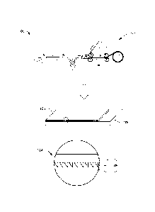
[0019] FIG. 1 is a schematic diagram of an illustrative environment 100 that
shows
an end-to-end process of manufacturing internal cavity optics for use with an
electronic display. A manufacturing apparatus 102 may be used to create small
optical cavities on medium carrier (e.g., a thin film). The small cavities may
be in the
range of micrometers to nanometers and may be created in various patterns
depending
on design requirements and a desired utility of the optics created using the
manufacturing apparatus 102. In some embodiments, the manufacturing apparatus
102 may be a roll-to-roll processing machine (or assembly); however, other
manufacturing techniques and apparatus may be used to perform lithography,
micro-
molding, or casting on a medium carrier.
[0020] In various embodiments, the manufacturing process may include
laminating
two or more layers of material together such that the cavities on a surface of
the
medium carrier are enclosed within and internal to the resultant laminated
material
104. The resultant laminated material 104 may be cut or trimmed in size to
overlay a
front or a back of a display 106. The resultant laminated material 104 may
perform
4
CA 02795265 2012-10-02
WO 2011/127187
PCT/US2011/031440
some or all functions of a frontlight or a backlight when positioned proximate
the
display 106.
[0021] The resultant laminated material 104 may include internal cavity optics
108,
which is shown by illustrative shapes in a detailed view in FIG. 1. The
internal cavity
optics 108 may be formed by the manufacturing apparatus 102 (e.g., roll-to-
roll
embossing/imprinting, etc.). In some embodiments, the internal cavity optics
108 may
be filled with air or another gas, a fluid, or a solid that enables the cavity
to redirect
light or otherwise modify a beam of light in accordance with intended design
requirements. The use of air in the cavities may enable formation of low
refractive
index performance, which may be useful in the production of optics. The
internal
cavity optics 108 may be formed in a carrier medium 110, which may be joined
by
lamination to a joiner medium 112 to form the resultant laminated material
104. The
seam, or surfaces, between the carrier medium 110 and the joiner medium 112
may be
fused together during the lamination such that the resultant laminated
material 104
appears as a single piece of material that includes the internal cavity optics
108. By
using the lamination process as described herein, internal cavity optics may
be created
that include inverted geometry when viewed from the display side (e.g.,
cavities with
a small opening or no opening) that may otherwise be impossible to create
using
imprinting, lithography or other similar techniques because of an inability to
remove a
tool from the cavity (e.g., inverted "v" feature) or otherwise control removal
of
material during manufacturing. However, these features become viable options
after
lamination of the two or more layers of material because the resultant
laminated
material 104 may be flipped over (inverted) and then applied to the display
106
because either side of the resultant laminate material may be suitable for
exposure to
elements (e.g., a user's finger, etc.).
CA 02795265 2012-10-02
WO 2011/127187
PCT/US2011/031440
[0022] In addition, the resultant laminated material 104 may include smooth
and
durable surfaces, which may prevent accumulation of dirt or other debris in
the
internal cavity optics 108. The resultant laminated material 104 may enable
input of
touch sensitive commands when implemented as a frontlight or otherwise protect
the
internal cavity optics during interaction by a user.
[0023] FIG. 2 is a schematic diagram of an illustrative manufacturing
apparatus 200
to create an internal cavity optical film that includes multiple layers of
material that
are laminated together. Although other techniques and apparatuses may be used
to
create the internal cavity optics 108, the manufacturing apparatus 200 is
discussed as a
roll-to-roll manufacturing apparatus that combines at least two layers of
material (e.g.,
the carrier medium 110 and the joiner medium 112).
[0024] The manufacturing apparatus 200 may include a roll of the carrier
medium
110 that is unwound from a source roller 202 during a manufacturing process.
In
accordance with various embodiments, the carrier medium 110 may be between a
few
nanometers thick up to a few millimeters thick depending on a desired
application.
The carrier medium 110 may be flexible or bendable and may be formed of a
polymer,
elastomer, glass, ceramic, or other flexible material that may be transparent,
semi-
transparent, or possibly translucent.
[0025] The carrier medium 110 may pass through a coater 204 that dispenses a
lacquer onto at least the surface of the carrier medium that is to receive the
cavities.
The lacquer may be curable by exposure to ultraviolet (UV) light (UV curable
lacquer), thermal exposure (thermo curable lacquer), moisture (moisture
curable
lacquer), electron beams (electron curable lacquer), or by other techniques.
The
carrier medium 110 may then pass across a replication cylinder 206 (or other
type of
shaped stamp) that contains patterns (ridges, features, etc.) that form
(emboss) the
carrier medium to create the cavities when the carrier medium passes over (or
under)
6
CA 02795265 2012-10-02
WO 2011/127187
PCT/US2011/031440
the replication cylinder. In accordance with some embodiments, the replication
cylinder 206 may include patterns on the scale of a few nanometers to a few
micrometers in width and/or height, which after interaction with the carrier
medium
110, create cavities of similar dimensions.
[0026] During and/or after the embossing, the carrier medium 110 may be cured
using a curing process 208 to cure the lacquer, which now may contain the
cavities
formed using the patterns of the replication cylinder 206. The curing process
may
include exposing the lacquer to UV light, thermal waves, moisture, electron
beams, or
any combination thereof, either sequentially or in simultaneously. The carrier
medium 110 may then pass through a main drive 210 that pulls the carrier
medium
from the source roller 202.
[0027] Meanwhile, the joiner medium 112 may be dispensed from another roller
212 and may be joined (overlapped) with the carrier medium to cover over the
cavities.
In some embodiments, the joiner medium 112 may be a thicker medium than the
carrier medium 110. For example, the joiner medium may be formed of plastic or
other material. In various embodiments the joiner medium 112 may be formed of
the
same material as the carrier medium 110, but may have a different thickness.
The
joiner medium 112 may be laminated to the carrier medium 110 by another curing
process 214. As discussed above, the lamination may fuse the materials
together to
effectively remove a seam between the materials. The resultant laminated
material 104
may pass through another set of drive rollers 216 and then be collected at a
depository
roller 218.
[0028] Although the manufacturing apparatus 200 only shows creation of the
internal cavity optics on a single carrier medium, the manufacturing device
may
include additional source rolls and replication cylinders/stamps to create
other layers
that, when processed through the replication cylinders, include the cavities.
These
7
CA 02795265 2012-10-02
WO 2011/127187
PCT/US2011/031440
additional layers may then be laminated together to create a resultant
laminated
material formed of multiple layers, which may include various layers of
internal
cavity optics. For example, one layer of the internal cavity optics may act as
a light
polarizer while another layer may include internal cavity optics as surface
relief
patterns or light management gratings that redirect light onto a display.
[0029] FIG. 3 is a flow diagram of an illustrative process 300 to laminate
multiple
layers of film together to enclose optical cavities within the film. The
process shows
the carrier film 110 prior to formation of the cavities at 302. After the
carrier film 110
passes over the replication cylinder 206 and is exposed to the curing process
208
during a pre-curing process, the carrier medium emerges at 304 with the
cavities.
[0030] The carrier medium 110 may then be joined with the joiner medium 112 at
a
lamination cylinder 306, which may laminate the carrier medium 110 to the
joiner
medium 112 at 308. Finally, the resulting laminated material may be exposed to
the
other curing process 214 during a post curing process at 310.
[0031] The process 300 may be arranged to enable application of the carrier
medium 110 on a relatively stiff joiner medium 112, which may be processed
while
remaining relatively flat or planar (as shown in FIG. 3). However,
other
configurations of the manufacturing apparatus 200 and/or the process 300 may
be
used to orient, process, handle, or otherwise manipulate the raw materials
prior to or
during the manufacturing to create the resultant laminated material 104 that
conforms
with design requirements.
[0032] FIG. 4 shows a schematic diagram of illustrative internal cavity optics
400
that may be created using the manufacturing apparatuses and processes shown
and
described in FIGS. 2 and 3. The illustrative cavity optics 400 may include
geometric
profiles, (shown in a first sample 402 and a second sample 404), a depression
profile
(shown in a third sample 406, a fourth sample 408, and a fifth sample 410), or
other
8
CA 02795265 2012-10-02
WO 2011/127187
PCT/US2011/031440
variations, such as a multi-pattern sample 412. Each configuration or sample
may
include specifically shaped and oriented cavities to redirect or otherwise
modify the
transmission of light from a light source in accordance with design
requirements.
[0033] In accordance with various embodiments, small patterns such as
gratings,
binary, blazed, slanted and trapezoid shapes may be formed by the
manufacturing
apparatus to create internal cavity optics having one or more of these
patterns. The
patterns may be discrete patterns, such as grating pixels, small recesses or
continuous
pattern forms, elongated recesses and channels, and/or any kind of two or
three
dimensional (2D, 3D) shapes. The pattern may include at least a small amount
of flat
surface on a contact surface to be laminated to enable proper adhesion and
light
propagation to the joiner medium. If there is no contact surface, the real air
cavity
may not be maintainable in some instances. For example, a round micro-lens
surface
may not form cavities that can withstand repetitive use. However, those
cavities may
be filled with a pressurized gas, a fluid or a solid, particularly when the
cavities are
created as long channels.
[0034] FIG. 5 is a flow diagram of an illustrative process 500 to laminate two
or
more films together to create an internal cavity optical film. The operations
described
in the process 500 may be performed using the manufacturing apparatus 200. The
process 500 includes a first sub-process 502 and a second sub-process 504. The
first
and second sub-processes may be performed independently or in parallel
(simultaneous or nearly simultaneous). In some embodiments, the process 500
may
only include the sub-process 502 and may refrain from performing some or all
of the
operations in the second sub-process 504. Additional sub-processes may also be
included in the process 500, which may perform the same or similar operations
as
described with respect to the first or second sub-processes.
9
CA 02795265 2012-10-02
WO 2011/127187
PCT/US2011/031440
[0035] In the first sub-process 502, at 506, the source roll 202 may dispense
or
unwind the carrier medium 110 (e.g., a thin foil, etc.). At 508, the carrier
medium 110
may be coated with a lacquer. For example, the coater 204 may spray the
carrier
medium 110 with the lacquer, the carrier medium 110 may be immersed, or
partially
immersed, in the lacquer, or the lacquer may be applied to the carrier medium
by other
techniques.
[0036] At 510, the replication cylinder 206 may emboss the carrier medium 110
to
create a pattern "A", which may be an optical pattern for a polarizer, an
incoupling/outcoupling pattern, a light management grating pattern, a surface
relief
pattern, a lens pattern, or another type of optical feature or pattern.
[0037] At 512, the curing process 208 may perform a pre-curing of the pattern
"A"
created by the embossing via the replication cylinder 206.
[0038] At 514, a side of the carrier medium 110 that includes the pattern may
be
joined with the joiner medium 112. The carrier medium 110 may then be
laminated to
the joiner medium 112 at 514.
[0039] At 516, the other curing process 214 may emit UV light (or other curing
process) onto the carrier medium 110 and joiner medium 112, which is
collectively
referred to as laminate "A" (i.e., the resultant laminated material 104).
[0040] The process 500 may end at 516 in embodiments where the resultant
laminated material 104 only includes two layers. However, additional layers,
and
therefore additional optical patterns of internal cavity optics may be added
to the
laminate "A" via the second sub-process 504 as explained below. The second sub-
process 504 may be performed prior to, after, or concurrently with the
operations of
the first sub-process 502.
[0041] At 518, another source roller (e.g., the roller 212) may dispense or
unwind
another carrier medium that may be the same as the carrier medium 110 used in
the
CA 02795265 2012-10-02
WO 2011/127187
PCT/US2011/031440
sub-process 502 or may be formed of another material and/or thickness. At 520,
a
coater (e.g., the coater 204) may coat the carrier medium with a lacquer. At
522, a
replication cylinder (e.g., the replication cylinder 206) may emboss the
carrier
medium to create a pattern "B", which may be a different optical pattern than
the
pattern "A". At 524, the curing process 208 may perform a pre-curing of the
pattern
"B" created by the embossing.
[0042] In some embodiments, some of the operations in the second sub-process
504
may be performed by the same or similar components that perform the operations
of
the first sub-process 502. In various embodiments, the manufacturing apparatus
may
include dedicated hardware to concurrently perform the first and second sub-
processes
502, 504.
[0043] At 526, the carrier medium with the pattern "B" may be joined with the
laminate "A" such that a side of the carrier medium with the pattern "B" is
joined with
and adjacent to a side of the laminate "A" to cover the cavities that form the
pattern
"B". Thus, the cavities in that form both the pattern "A" and the pattern "B"
are
internal cavities after lamination. The carrier mediums may be laminated
together at
516 to create a single material (e.g., the resultant laminate material 104
having
multiple layers of internal cavity optics). At 528, the resultant laminate
material 104
may undergo a post-curing process to cure the laminate.
[0044] In some embodiments, additional sub-processes that are similar to the
second sub-process 504 may be performed to add additional layers, and thus
additional layers of internal cavity optics to the resultant laminate material
104.
[0045] FIGS. 6a-6c show schematic diagrams of various internal cavity optic
solutions that may be implemented in frontlights and/or backlights for
electronic
displays. FIG. 6a shows an assembly 600 that includes the display 106 having a
resultant laminate material 104 having a single layer of internal cavity
optics that are
11
CA 02795265 2012-10-02
WO 2011/127187
PCT/US2011/031440
applied to a front side of the display. For example, the resultant laminate
material 104
may be used in this configuration as a frontlight. Additional details of the
frontlight
configuration are discussed below with reference to FIGS. 10a and 10b. The
resultant
laminate material may alternatively be used in this configuration as a
backlight, which
is described with additional details with reference to FIGS. 9a-9e.
[0046] FIG. 6b shows an assembly 602 that includes the display 106 having a
first
resultant laminate material 604 having a layer of internal cavity optics and
that are
applied to a front side of the display 106 and a second resultant laminate
material 606
having a layer of internal cavity optics that are applied to a back side of
the display
106.
[0047] FIG. 6c shows an assembly 608 that includes the display 106 having a
multi-
layer resultant laminate material 610 having multiple layers of internal
cavity optics
612 and that are applied to a side of the display 106.
[0048] FIG. 7 is a flow diagram of an illustrative end-to-end process 700 of
manufacturing the internal cavity optics. The process 700 includes three sub-
processes. A first sub-process 702 describes molding to create at least a
portion of the
manufacturing apparatus 102, a second sub-process 704 describes use the
manufacturing apparatus 102, and a third sub-process 706 describes material
processing and quality control processing of the resultant laminated material
104.
Each of the sub-processes is described in turn.
[0049] In accordance with various embodiments, the first sub-process 702 may
include an optical design at 708 and master fabrication at 710. A nickel shim
may be
created at 712, which may be used to, or implemented as, a production tool at
714.
The nickel shim may be attached to the manufacturing apparatus at 716 to
enable the
embossing of the carrier medium 110.
12
CA 02795265 2012-10-02
WO 2011/127187
PCT/US2011/031440
[0050] In some embodiments, a pre-mastering pattern may be completed by micro
machining, lithography, imprinting, embossing or other suitable techniques.
The pre-
mastering pattern can be replicated by electroforming, casting, or molding.
The
formed nickel, plastic master plate, cast material plate, or molded plate may
be formed
to contain a plurality of micro-reliefs that create a pattern on the surface
of the plate.
The pattern may include one or more of small grooves, recesses, dots, pixels,
and so
forth. In some embodiments, the micro-reliefs (or non-reliefs) are negative
relief
patterns that may be suitable for an inkjet printing modulation process. This
modulation process may be based on a profile filling technique in which an
existing
groove, recess, dot, pixel, etc. is completely filled with inkjet/printed
material. This
material may be dispensed in the master plate by forming small pico (10-12)
drops in
order to fill and "hide" the existing patterns. The techniques may be suitable
to
complete a filling factor modulation on the surface (e.g., in a lightguide
application,
etc.). However, these techniques may be suitable for many other applications
as well,
and not only for completing filling factors. It may also be used to design
different
discrete figures, icons, forms and shapes, which enable creation of a low cost
optical
designing process that is relatively fast, flexible, and easy to use. These
techniques
may be particular well adapted for large surface areas (e.g., a large screen
monitor or
television, etc.).
[0051] The filling material (e.g., ink, etc.) may be transparent and optically
clear,
which may have the same or a similar refractive index as the plate material.
This may
enable real functional testing. In some embodiments, colored ink may be used.
However, the use of colored ink may require a replication process in order to
obtain
functional optical testing of a completed part.
[0052] A drop size and material viscosity are also important considerations in
terms
of controlled and high quality filling. If a viscosity is too low, the drop
may flow for a
13
CA 02795265 2012-10-02
WO 2011/127187
PCT/US2011/031440
large area and may travel along a bottom of a groove, thus making it difficult
to
completely fill a structure. If the viscosity is too high, the drop size may
be larger, but
the form is more compact and may not flow on the groove as much as desired.
[0053] A low viscous material, which guarantees small drop size, may be a good
tradeoff When utilizing a small pattern, discrete grooves, recesses, dots or
pixels, the
drop may be used to fill only preferred patterns in a preferred location.
Thus, a pre-
master structure is preferable patterned with small pixels or discrete
profiles.
[0054] In accordance with some embodiments, the second sub-process 704 may
include loading the carrier medium 110 and joiner medium 112 at 718. At 720,
the
manufacturing apparatus 102 may unwind the carrier medium 110, which may
undergo web cleaning and deionization at 722. At 724, the carrier medium may
be
treated with lacquer. At 726, the carrier medium 110 may be embossed by
replication
cylinder 206 and pre-cured with the light. At 728, the carrier medium, once
embossed,
may be inspected for quality control (QC) purposes and re-reeled (rolled for
storage).
At 730, the embossed carrier medium may be unloaded from the manufacturing
apparatus 102. In some embodiments, the second sub-process 704 may include the
lamination as described in the operations 514 and 516 of the first sub-process
502
shown in FIG. 5.
[0055] In accordance with various embodiments, the third sub-process 706 may
include unwinding the resultant laminated material that includes the internal
cavity
optics at 732. At 734, the resultant laminated material may be laminated to a
side of a
display, a lightguide, or other feature. At 736, the resultant laminated
material may be
cut using laser cutting, die cutting, or other cutting techniques. For
example, excess
material may be cut from edges of a display or lightguide after the material
is attached
to the display. At 738, excess material may be removed, such as the material
cut in
the operation 736. At 740, excess material may be re-reeled and stored for
later use.
14
CA 02795265 2012-10-02
WO 2011/127187
PCT/US2011/031440
[0056] At 742, the material may be tested for quality control purposes. For
example, the material may be deployed as a frontlight or backlight with an
electronic
display and then measurements may be taken to determine whether the material
is
suitable for further deployment. At 744, a tray may be assembled.
Illustrative Optics
[0057] FIG. 8 is a schematic diagram of illustrative implementations of the
internal
cavity optics 800 that includes variations arranged in a hierarchy. The
internal cavity
optics 800 may be subdivided into light directing films 802 and lightguide
plates 804.
The light directing films 802 may be thin films that are laminated or
otherwise
attached or configured adjacent to a display or lightguide to direct light
from a light
source in accordance with design requirements. For example, the light from a
light
source may be directed through the films that include surface relief forms,
light
management gratings, a polarizer, or other optical features that manipulate
the light
and/or re-direct the light onto or through individual pixels of a display. As
shown in
FIG. 8, the light directing films 802 may include front display illumination
806 and
back display illumination 808 as different configurations of the light
directing films
802.
[0058] The internal cavity optics 800 may also be deployed as the lightguide
plates
804. The lightguide plates 804 may direct light from a light source to
disperse the
light across a surface of the display. For example, the lightguide plates 804
may
include surface relief forms deployed as the internal cavity optics. The
lightguide
plates 804 may be configured as a display frontlight 810 and/or as a display
backlight
812. Each of the configurations of the internal cavity optics 800 will be
described in
further detail with reference to the following figures.
Illustrative Backlight Configurations
CA 02795265 2012-10-02
WO 2011/127187
PCT/US2011/031440
[0059] FIGS. 9a-9e are schematic diagrams of illustrative backlights that use
the
internal cavity optics. Lightguides may be produced from bulk plates or films,
which
may have laminated film on a surface (one side or both sides). The film may
include
optical patterns, which outcouple the light for distribution. Pre-formed films
may be
laminated, which include the internal cavities on the laminated surfaces.
These
formed cavities may comprise air (or another gas) and thus may provide low
refractive
index properties and very effective outcoupling and light managing features.
[0060] FIG. 9a shows an illustrative transparent lightguide 900 with laminated
coupling optics. A resultant laminated material 902 may include coupling
patterns
904. The resultant laminated material 902 may be laminated to the lightguide
via a
rolling process or other suitable process (adhesives, etc.).
[0061] FIG. 9b shows an illustrative transparent lightguide 908 that includes
internal cavity optics. The resultant laminated material 910 may include
internal
cavity optics 912 in a profile of internal microcavity coupling optics or
nanocavity
coupling optics. In some embodiments, the internal cavity optics 912 may be
filled
with air. However, other fluids, gases, or solids may be used to fill the
cavities. In
some embodiments, the resultant laminated material 910 may include at least
one
layer formed of glass or plastic, which may be the joiner medium 112 and more
rigid
than the carrier medium 110 that is embossed with the cavity optics prior to a
lamination of the mediums to form the resultant laminated material 910 having
the
internal cavity optics 912.
[0062] FIG. 9c shows an illustrative transparent lightguide 914 that includes
internal cavity optics. A resultant laminated material 916 may include a first
layer
918 of internal cavity optics to couple and/or collimate light beams and a
second layer
920 of cavity optics that act as a polarizer. In some embodiments, the
polarizer may
16
CA 02795265 2012-10-02
WO 2011/127187
PCT/US2011/031440
use a wire grid profile. The polarizer may be implemented as internal cavity
optics in
the second layer 920 or on a surface of the resultant laminated material.
[0063] In various embodiments, the top laminated film (second layer 920) may
contain integral light outcoupling optics and polarization gratings (wire grid
or other
new grating solution) on the top of the film. This may be a beneficial
solution for
liquid crystal display (LCD) technologies because narrow light outcoupling and
distribution in on-axis may be a most suitable direction for top polarization
gratings
and provides a high degree of polarization, which may not be based on light
circulation. This may provide higher efficiency of the polarized light. This
film
solution can be further laminated directly to the display backplate together
with
lightguide plate.
[0064] FIG. 9d shows an illustrative display 922 that includes internal cavity
optics
configured to create a hollow backlight with internal cavity coupling optics
(e.g.,
integrated wire grid polarizer, etc.). A resultant laminated material 924 may
include
an adhesive layer 926 on a backplate 928 of the display 922. An integrated
wire grid
polarizer 930, coated binary profile may be applied adjacent to the adhesive
layer 926.
A laminated film 932 with a profile of coupling optics may be applied adjacent
to the
integrated wire grid polarizer 930. A reflector 934 may be separated from the
laminated film 932 by a cavity 936 filled with air, another gas, a fluid, or a
solid.
[0065] FIG. 9e shows an illustrative lightguide 938 that includes internal
cavity
optics. A resultant laminated material 940 may include coupling patterns 942
with a
vertical contact grid while the lightguide 938 may include a horizontal
contact grid
944. The lightguide 938, with the resultant laminated material 940, may be
configured as active cavity coupling optics by a passive matrix grid formed
with the
coupling patterns 942 and the horizontal contact grid 944.
17
CA 02795265 2012-10-02
WO 2011/127187
PCT/US2011/031440
[0066] As shown in FIG. 9e, the backlight may be formed by a hollow type of
lightguide, in which the air is a medium carrier and grating pattern (positive
relief) is
coupling light directly. This type of grating film can be laminated on another
medium
carrier such as plastic or glass plate. In some embodiments, the grating film
may be
directly laminated on the backplate of the display. This integrated solution
may
enable production of a thinner lightguide that previous lightguides.
[0067] In some embodiments, polarizer gratings may be applied on a side of the
film, which may be on a contact of a backplate of a display. The ordering of
layers
may be arranged as 1) light directional coupling, 2) polarization, and 3)
display
transmission or other variations of this combination.
[0068] This solution may effectively mix light emitting diode (LED) light if
there
are different color ranks. For a larger lightguide solution, there may be
little or no
light absorption of medium catTier (like plastic has) and a shift of a color
coordinate
of the white light. If coupling patterns are based on linear orientation, pre-
collimation
optics for the LED sources may be beneficial.
[0069] The above discussion is primarily based on edge lighting solutions.
However, the described hollow lightguide can also be created with several LED
rows
under the film. Then LEDs are collimated or reflected by 3D reflectors in
order to
achieve uniformity. This type of coupling can be utilized also for light
incoupling.
[0070] In some embodiments, lightguides can be made with the optical film
described above, which has active/passive matrix (electrical, such as TFT
technology)
for surface contact control, which may also be based on cavity optics. This
electrically controlled system may provide outcoupling in the designated
location (via
software) at preferred time. Software may control the uniformity and density
of
coupling contact factors in order to control uniformity and brightness.
Electrical
18
CA 02795265 2012-10-02
WO 2011/127187
PCT/US2011/031440
contacts can be based on static electricity or other viable solutions. This
solution is
suitable for an LED display (e.g., television, etc.) and/or a light panel.
[0071] In accordance with some embodiments, infrared (IR) based coupling may
be
achieved using the internal cavity optics with visible light. Dual layers may
be
utilized, such as an inner layer for visible light coupling and an outer layer
for IR light
coupling (air gap). Low refractive index coating/film for IR coupling may be
utilized,
which has lower thickness than IR light. Thus, the visible light may be unable
to
"see" IR patterns and only IR light can see them because of a thickness of the
layer.
This is one suitable solution for an IR-based touch screen. A touch screen
circuit
(e.g., with ITO or carbon nanotubes) can be printed on a top surface, which
may
create a more integrated solution. This may be used for backlight and/or
frontlight
applications.
Illustrative Frontlight Configurations
[0072] FIGS. 10a and 10b are schematic diagrams of illustrative frontlights
that use
the internal cavity optics. The frontlight may be a separate element on the
top of a
display. Frontlight solutions often have problems with contrast and reflection
between
surfaces caused by stray light. Use of a laminated frontlight with a lower
refractive
index material between the lightguide and display substrate may improve
contrast and
reduce reflections between the surfaces.
[0073] FIG. 10a shows an illustrative display 1000 that includes internal
cavity
optics. A resultant laminated material 1002 may include a plain surface 1004,
which
protects internal cavity optics 1006 from contamination, debris, or other
matter that
may impair the optical quality of the resultant laminated material 1002. The
resultant
laminated material 1002 may be attached to the display 1000 via an adhesive
layer
1008 on the top plate of the display 1000. The adhesive layer 1008 may be
adjacent to
19
CA 02795265 2012-10-02
WO 2011/127187
PCT/US2011/031440
the carrier medium 110 that includes the internal cavity optics 1006 while the
plain
surface 1004 may be part of the joiner medium 112, which may be formed of a
plastic
or glass material or other relatively sturdy material that resists damage and
protects
the internal cavity optics 1006.
[0074] In some embodiments, optical coupling patterns may be placed on the
backplate. Normally these patterns are on the top surface of the display,
which can
lower a contrast especially when there is a larger amount of the stray light.
When the
patterns are placed close to the real display image, the visibility of the
patterns is
lessened, which enables utilization of higher density structures and even
larger
structures and profiles without sacrificing visibility. The bottom pattern may
be
integrated by lamination on the display or image surface. Bottom patterns may
minimize stray light while enable use of other functional patterns or layers
on the top
of the frontlight, such as anti-reflection pattern, anti-clear pattern, touch
screen
element (circuits, layers), other optical patterns/films (polarizer gratings),
and so forth.
A plain top surface is may be appropriate for "open" solutions where users
interact
with the display using touch commands.
[0075] Optical patterns for the frontlight may be created using small optical
patterns
(nano/micro scale) such as gratings. Binary gratings are effective for a
larger viewing
angle and blazed gratings are often effective for a narrower viewing angle. A
hybrid
grating solution that combines these solutions may also be utilized.
[0076] Electronic paper displays, in particular, rely on use of adequate
frontlighting,
which may be provided by frontlights that include internal cavity optics.
These types
of displays, in which the image surface is very close to the top plate/film,
function
well with binary gratings or other invisible pattern frontlights. Optical
patterns may
be made to be practically invisible to humans by lamination of film/adhesive
film,
which completely penetrates in the grating profile.
CA 02795265 2012-10-02
WO 2011/127187
PCT/US2011/031440
[0077] Light incoupling is a consideration when a laminated frontlight is
used.
Normally lamination forms brighter spots (hot spots) in an area in the
vicinity of light
source. This can be avoided or minimized using a tape strip or printed strip
on the
front of light source. Also some diffusing optics patterns can be utilized.
These
solutions avoid the hot spot and provide more uniform illumination from the
light
source or light sources.
[0078] FIG. 10b shows an illustrative display 1010 that includes internal
cavity
optics. A resultant laminated material 1012 may include the internal cavity
optics
1006 and an adhesive layer 1008. In addition, the resultant laminated material
1012
may include a surface laminated touch panel 1114 to configure the frontlight
as a
touch integrated frontlight solution. The frontlight structure may be formed
with a
light outcoupling structure and a touch screen circuit or IR coupling
structure in a
same lightguide. Structures can be placed on the same side or different sides
of the
lightguide. The visible light may have its own outcoupling pattern and the IR
coupling pattern and/or the touch circuit may be separated or isolated by an
individually placed layer, which may be implemented using a side laminated
layer or
two different laminated layers (one side or both sides). In some embodiments,
white
light may be utilized for the touch screen solution. This is based on optical
signal
strengthening using coupling optics. The touch screen solutions may be
suitable for
electronic book reader devices, mobile phones, and/or other consumer
electronics that
include a display.
[0079] FIGS. lla-lld are schematic diagrams of illustrative configurations of
the
internal cavity optics implemented on two or more layers that are laminated
together
to create a resultant laminated material.
[0080] FIG. lla shows a side view of an illustrative resultant laminated
material
1100 that includes example rays of light 1102 being redirected by internal
cavity
21
CA 02795265 2012-10-02
WO 2011/127187
PCT/US2011/031440
optics 1104, where the rays of light are emitted by a light source from a
single side of
the resultant laminated material. The internal cavity optics 1104 may be
surface relief
patterns to redirect the light as collimated light or another type of light.
[0081] FIG. 1 lb shows a side view of another illustrative resultant laminated
material 1106 that includes example rays of light 1108 being redirected by
internal
cavity optics 1110. The internal cavity optics 1110 may be gratings to
redirect the
light as colored light or otherwise disperse the light onto an adjacent
surface (e.g., a
display). The internal cavity optics 1110 may also be a polarizer or other
optical
feature or pattern.
[0082] FIG. 11c shows a side view of yet another illustrative resultant
laminated
material 1112 that includes example rays of light 1114 being redirected by
internal
cavity optics 1116, where the rays of light are emitted by multiple light
sources from
either side of the resultant laminated material 104. The internal cavity
optics may be
surface relief patterns to redirect the light as collimated light or another
type of light.
[0083] FIG. 1 ld shows a side view of an illustrative resultant laminated
material
1118 having multiple layers. A first layer 1120 may include internal cavity
optics that
provide a polarizer, a second layer 1122 may include internal cavity optics
that
provide redirection of light form a lightguide, and a third layer 1124 of
internal cavity
optics may provide other optical effects (e.g., lens, incoupling, etc.). More
or fewer
layers may also be included in the resultant laminated material 1118, which
may be
created using the process described with reference to FIG. 5.
Other illustrative Implementations
[0084] In some embodiments, the internal cavity optics may be used to create
lenses.
Laminated lens film may form cavity coupling structures on a scale of
micrometers to
nanometers. Embossed/imprinted films can be laminated on the carrier medium to
22
CA 02795265 2012-10-02
WO 2011/127187
PCT/US2011/031440
produce lens structures with multiple layer patterns. The optical patterns may
be
completely integrated/embedded and are thus protected from debris or damage.
There
are many applications for these lenses such as in halogen replacements, solar
cell
concentrators, and general lighting implementations.
[0085] Another illumination lens is an un-direct transmission element, which
is a
coupling light from the air medium that directs the light at predetermined
angles. In
some embodiments, some surfaces have reflectors (2D or 3D) and other surfaces
have
a coupling pattern (2D or 3D). An LED bar may be used to collimate light at
least in a
2D horizontal direction. Another application is a light bar, rod or tube, in
which the
coupling structure or film is an outer surface or an inner surface for
coupling and
directing the light. In the tube solution, a reflector rod can be utilized in
the center
(inner part). This type of coupling film can be laminated and direct light for
various
angles (inside or outside). The structure may be volume integrated, which may
keep
the pattern free from defects. Grating lenses may also provide an improved
efficiency
over conventional Fresnel lenses due to having smaller features, which have
much less
back reflection than conventional larger patterns, and also because a location
of the
patterns on a bottom side. When the patterns are on the bottom side, there is
less direct
back reflection because the medium carrier is on the top side.
[0086] In accordance with some embodiments, the internal cavity optics may
also
be used in a film to provide collimated light, or otherwise referred to as
"collimation
film." A laminated cavity coupling film may provide a more narrow
illumination.
Larger incident angles can be collimated for the narrow angle and small angles
can be
transmitted through this film without a noticeable efficiency drop. Optical
patterns
can be nearly invisible in a display solution. These patterns may also be
integrated or
embedded by lamination. Additionally a LCD can have this type film on the top
side,
which may result in a more narrow distribution of light. The LCD normally
makes
23
CA 02795265 2012-10-02
WO 2011/127187
PCT/US2011/031440
distribution a bit larger even when prism sheets are utilized in the
backlight. The
transparent film with the internal cavities may be utilized on the top side
and provide a
final distribution of light.
[0087] In various embodiments, the internal cavity optics may also be used as
a
polarizer. A grating polarizer or wire grid can be produced by roll-to-roll
techniques
discussed above or other manufacturing techniques. In some embodiments, basic
profiles may be manufactured by curing, and then deposition coating may be
performed by a higher refractive index by means of laser assisted deposition,
automatic layer deposition (ALD), or other similar techniques. The laser can
deposit
many different materials. Orientated directional deposition (on side
deposition,
asymmetric) may be used. The grating profile can be binary, slanted, quadrate
with
different slanted surfaces, and so forth.
[0088] In some embodiments, the internal cavity optics may also be used for
light
incoupling. A flat ball lens bar, especially on a row is a unique solution,
and may
contain a 2D surface or a 3D surface, depending on a collimation axis.
Principally
one axis collimation is adequate. This optical solution may be produced
separately or
together with a lightguide. Manufacturing techniques may include injection
molding,
casting, laser cutting, and so forth.
Conclusion
[0089] Although the subject matter has been described in language specific to
structural features and/or methodological acts, it is to be understood that
the subject
matter defined in the appended claims is not necessarily limited to the
specific
features or acts described. Rather, the specific features and acts are
disclosed as
illustrative forms of implementing the claims.
24