Note: Descriptions are shown in the official language in which they were submitted.
CA 02795315 2012-10-03
1
WO 2011/127980
PCT/EP2010/054974
HYBRID 2-LEVEL AND MULTILEVEL HVDC CONVERTER
This invention relates to a voltage source converter for use in
high voltage direct current (HVDC) power transmission and reactive power
compensation, and a method of operating a voltage source converter.
In power transmission networks alternating current (AC) power
is typically converted to direct current (DC) power for transmission via
overhead
lines and/or undersea cables. This conversion removes the need to compensate
for
the AC capacitive load effects imposed by the transmission line or cable, and
thereby reduces the cost per kilometer of the lines and/or cables. Conversion
from
AC to DC thus becomes cost-effective when power needs to be transmitted over a
long distance.
The conversion of AC to DC power is also utilized in power
transmission networks where it is necessary to interconnect AC networks
operating at different frequencies. In any such power transmission network,
converters are required at each interface between AC and DC power to effect
the
required conversion, and one such form of converter is a voltage source
converter
(VSC).
AC power is typically transmitted in the form of one or more
sinusoidal waveforms depending on the number of AC phases. The presence of
sinusoidal AC waveforms on the AC side of the voltage source converter can
however lead to high levels of DC voltage ripple in the DC side of the voltage
source converter and the associated DC network.
The presence of DC ripple in the DC network prevents the use of
low cost cables, which are generally intolerant of alternating voltage stress,
and
thereby increases installation costs of DC power transmission lines. In
addition,
the alternating nature of the DC ripple leads to undesirable interference
between
the DC power transmission lines and nearby telephone lines, which increases
the
complexity of designing the layout of DC power transmission lines.
Conventionally, power stations utilize DC filtering equipment
such as passive inductive and capacitive elements on the DC side of the
voltage
CA 02795315 2012-10-03
2
WO 2011/127980
PCT/EP2010/054974
source converter to minimise DC ripple. The use of parallel capacitance and
series
inductance in combination with the voltage source converter respectively leads
to
reduction of voltage and current ripple. The high voltage nature of power
transmission however means that it is necessary to employ large passive
inductive
and capacitive elements, which adds to the size, weight and cost of the
associated
power station. This is particularly undesirable in locations with limited
space
envelopes such as off-shore wind farms.
According to a first aspect of the invention, there is provided a
voltage source converter for use in high voltage direct current power
transmission
1 o and
reactive power compensation, the voltage source converter comprising first
and second DC terminals for connection in use to a DC network, three phase
elements and at least one auxiliary converter connected between the first and
second DC terminals, each phase element including a plurality of primary
switching elements and at least one AC terminal for connection in use to a
respective phase of a multi-phase AC network, the plurality of primary
switching
elements being controllable in use to facilitate power conversion between the
AC
and DC networks, the or each auxiliary converter being operable in use to act
as a
waveform synthesizer to modify a first DC voltage presented to the DC network
so
as to minimise ripple in the DC voltage.
The provision of the auxiliary converter results in a voltage
source converter with a flexible DC side active filter capable of synthesizing
a
range of waveforms having different shapes and sizes to minimise DC ripple,
which may vary depending on the characteristics of the AC and DC networks.
The reduction of DC ripple in the DC network not only reduces
installation costs by enabling the use of low cost cables which are normally
intolerant of alternating voltage stress, but also simplifies planning issues
associated with the DC network, such as location, by minimising undesirable
interference with telephone lines situated near the DC network.
The reduction of DC ripple in this manner also eliminates the
need for DC side filtering equipment in the form of passive inductive and
capacitive elements. This
removes the additional cost of installing and
CA 02795315 2012-10-03
3
WO 2011/127980
PCT/EP2010/054974
maintaining DC side filtering equipment, improves the reliability and
efficiency of
the associated power station by minimising the amount of converter hardware,
and
reduces hardware size and weight, which is desirable in locations with limited
space envelopes such as offshore power stations.
Preferably each phase element includes two parallel-connected
strings of series-connected primary switching elements, the mid-points between
each string of series-connected primary switching elements defining AC
terminals
for connection in use to a respective phase of the AC network.
Such a voltage source converter arrangement may be utilised to
facilitate power conversion between the AC and DC networks.
In other embodiments, the voltage source converter may include
three auxiliary converters connected between the first and second DC
terminals,
wherein each auxiliary converter is connected in parallel with a respective
one of
the phase elements to define a single-phase converter limb, and the three
single-
phase converter limbs are connected in series on the DC side of the circuit to
define a two-terminal DC network for three-phase power transmission.
In addition to being suitable for facilitating power conversion
between the AC and DC networks, this voltage source converter arrangement also
allows each auxiliary converter to be controlled so as to have direct
influence on
the phase connected to the AC terminal of the respective phase element and
limited influence on the other two phases connected to the AC terminals of the
other two phase elements.
In further embodiments, the or each auxiliary converter may be
operable in use to act as a waveform synthesizer to modify a second DC voltage
presented to the DC side of the respective phase element. In such embodiments,
the or each auxiliary converter may be operable in use to synthesize a near-
approximation of a rectified sinusoidal waveform for presentation to the DC
side
of the respective phase element.
The or each auxiliary converter may be used to shape the DC
voltage for transfer to the AC side of the voltage source converter. Otherwise
the
constant DC side voltage would produce a square wave voltage on the AC side of
CA 02795315 2012-10-03
4
WO 2011/127980
PCT/EP2010/054974
the or each phase element, with significant harmonic components and hard
switching of the semiconductor devices. The provision of one or more auxiliary
converters however allows for the production of a more desirable AC waveform
with less harmonic distortion, such as a sinusoidal waveform, and also enables
soft-switching of the semiconductor devices at low levels of voltage and
current.
In order to minimise DC ripple in the first DC voltage, the or
each auxiliary converter may be operable in use to synthesize a waveform
including at least one rectified, zero-phase sequence triplen harmonic
component
to cancel one or more harmonic ripple components in the first DC voltage.
1 o When the first DC voltage includes undesirable ripple
components of the first DC voltage in the form of harmonics of the AC supply
frequency such as 6th, 12th and 18th harmonics, the addition of higher order
zero-
phase sequence, triple harmonic components to the synthesized waveform cancels
out each harmonic ripple component and thereby minimises DC ripple in the
first
DC voltage. For example, inclusion of 9th and 15th harmonic zero-phase
sequence
components in the synthesized waveform respectively leads to the elimination
of
the 6th and 12th harmonic ripple components in the first DC voltage.
The zero-phase sequence nature of the harmonic components
means that when a transformer is used to interconnect the voltage source
converter
and the AC network, the effects of the additional modulation is limited to the
secondary side of the transformer connected to the voltage source converter
and
has no effect on the AC voltage and current at the primary side of the
transformer
connected to the AC network. As such, the introduction of zero-phase sequence
triplen harmonic components to minimise DC ripple has little detrimental
effect on
the AC network.
In order to minimise DC ripple in the first DC voltage, the or
each auxiliary converter may be operable in use to synthesize a waveform
including a DC voltage component and at least one harmonic AC voltage
component, each waveform operating at a phase difference of 120 electrical
degrees to the other two waveforms.
CA 02795315 2012-10-03
WO 2011/127980
PCT/EP2010/054974
The phase difference of 120 electrical degrees between the
synthesized waveforms means that the summation of the three synthesized
waveforms leads to the harmonic AC voltage components being cancelled out, and
thereby leaves a ripple-free DC side voltage consisting of the DC voltage
5 components.
Such waveforms are more straightforward to synthesize, which
simplifies control of the or each auxiliary converter when synthesizing the
waveform. Although the use of non zero-phase sequence harmonic AC voltage
components may result in low levels of harmonic distortion at the AC network,
the low levels of harmonic distortion may be acceptable in AC networks with
less
stringent power quality requirements.
In embodiments of the invention, the voltage source converter
may further include at least one tertiary converter, the or each tertiary
converter
being operable in use to act as a waveform synthesizer to modify one or more
second DC voltages, each second DC voltage being presented to the DC side of
the
respective phase element. In such embodiments, the or each tertiary converter
may be operable in use to synthesize a near-approximation of an offset
rectified
sinusoidal waveform for presentation to the DC side of the respective phase
element.
In embodiments employing the use of single-phase converter
limbs, each single-phase converter limb may include at least one tertiary
converter.
At least one tertiary converter may be connected in series with the phase
element
in the respective single-phase converter limb.
In other embodiments employing the use of tertiary converters,
the phase elements may be connected in a cascade arrangement to define a first
limb, three auxiliary converters may be connected in a cascade arrangement to
define a second limb, the first and second limbs being connected in parallel
on the
DC side of the circuit between the first and second DC terminals, and a
tertiary
converter may be connected between a respective one of the junctions between
the
phase elements and a respective one of the junctions between the auxiliary
converters.
CA 02795315 2012-10-03
6
WO 2011/127980
PCT/EP2010/054974
The provision of the or each tertiary converter allows the
generation of a desired AC waveform shape at the AC side of each phase element
irrespective of the waveform shapes synthesized by the or each auxiliary
converter. For example, when the auxiliary converter is used to synthesize
waveforms including non-zero-phase sequence AC components to modify the first
DC voltage and thereby minimise DC ripple, the or each tertiary converter can
be
controlled to modify the synthesized waveform to form an offset rectified
sinusoidal waveform for presentation to the DC side of the phase element. This
therefore allows the voltage source converter to simultaneously minimise DC
ripple and maintain high quality AC sinusoidal waveforms with minimal harmonic
distortion.
Preferably the or each tertiary converter and/or the or each
auxiliary converter include a chain-link converter. Such a chain-link
converter
may include a chain of modules connected in series, each module including at
least
one pair of secondary switching elements connected in parallel with an energy
storage device, the secondary switching elements being controllable in use so
that
the chain of modules connected in series presents a stepped variable voltage
source.
To define a 2-quadrant unipolar module that can provide zero or
positive voltage and can conduct current in two directions, the or each module
may
include a pair of secondary switching elements connected in parallel with the
energy storage device in a half-bridge arrangement.
To define a 4-quadrant bipolar module that can provide negative,
zero or positive voltage and can conduct current in two directions, the or
each
module may include two pairs of secondary switching elements connected in
parallel with the energy storage device in a full-bridge arrangement.
The structure of the chain-link converter allows the build-up of a
combined voltage, which is higher than the voltage provided by an individual
module, via the insertion of multiple modules, each providing a voltage, into
the
chain-link converter. By varying the value of the combined voltage, the chain-
link
CA 02795315 2012-10-03
7
WO 2011/127980
PCT/EP2010/054974
converter may be operated to generate a voltage waveform of variable amplitude
and phase angle.
Preferably each energy storage device includes a capacitor, fuel
cell, battery, photovoltaic cell or an auxiliary AC generator with an
associated
rectifier.
Such flexibility is useful in the design of converter stations in
different locations where the availability of equipment may vary due to
locality
and transport difficulties. For example, the energy storage device of each
module
on an offshore wind farm may be provided in the form of an auxiliary AC
generator connected to a wind turbine.
Each switching element preferably includes at least one
semiconductor device or includes a plurality of semiconductor devices
connected
in series. The or each semiconductor device may be an insulated gate bipolar
transistor, a field effect transistor, a gate turn-off thyristor, a gate
commutated
thyristor, an integrated gate commutated thyristor or a transistor.
In embodiments employing the use of semiconductor devices,
each semiconductor device may be connected in parallel with an anti-parallel
diode.
The use of semiconductor devices is advantageous because such
devices are small in size and weight and have relatively low power
dissipation,
which minimises the need for cooling equipment. It therefore leads to
significant
reductions in power converter cost, size and weight.
The fast switching capabilities of such semiconductor devices
allow the or each auxiliary converter to not only synthesize complex waveforms
when modifying the first and/or second DC voltages, but also to synthesize
high
quality waveforms to further minimise harmonic distortion and DC ripple
levels.
Furthermore the inclusion of such semiconductor devices allows the or each
auxiliary converter to respond quickly to changes in the AC and DC voltages
and
modify the synthesised waveforms accordingly.
In further embodiments, the or each auxiliary converter is
operable in use to synthesize a waveform including at least one rectified,
zero-
CA 02795315 2016-11-29
8
phase sequence triplen harmonic component to produce a compensatory DC
voltage to compensate for changes in the real and/or reactive power
requirements
on the AC side of the respective phase element.
In use, synthesis of the waveform may produce a negative
compensatory DC voltage component to compensate for an increase in the first
DC
voltage required to generate reactive power from the AC network or a positive
compensatory DC voltage component to compensate for a decrease in the first DC
voltage required to absorb reactive power from the AC network.
By controlling each auxiliary converter, it is possible to produce
a compensatory DC voltage component so as to ensure that the net increase or
decrease in the first DC voltage is controlled to be zero whilst the AC
voltage can
be made to vary in order to allow reactive power control.
According to a second aspect of the invention, there is provided a
method of controlling a voltage source converter including a plurality of
phase
elements connected between first and second DC terminals connected to a DC
network, the or each phase element including a plurality of primary switching
elements and at least one AC terminal connected to a respective phase of a
multi-
phase AC network comprising the steps of controlling the primary switching
elements to facilitate power conversion between the AC and DC networks and
modifying a DC voltage presented to the DC network to minimise ripple in the
DC
voltage.
Preferred embodiments of the invention will now be described,
by way of non-limiting examples, with reference to the accompanying drawings
in
which:
Figure 1 shows, in schematic form, a voltage source converter according to
a first embodiment of the invention;
Figure 2 shows the synthesis of a 50Hz sinusoidal waveform using a chain-
link converter;
CA 02795315 2012-10-03
9
WO 2011/127980
PCT/EP2010/054974
Figure 3 shows the ratio of the first DC voltage to fundamental component
of AC side voltage required to facilitate reactive power control for a voltage
source
converter and the required amount of 3rd harmonic modulation in the presence
of a
constant average first DC voltage, and the relative levels of 9th and 15th
harmonic
modulation required to totally eliminate the 6th and 12th harmonic ripple
components from the first DC voltage;
Figure 4 shows a synthesized waveform and the corresponding AC side
waveform for an operating condition near to 0.8 modulation index in which
large
amounts of 3rd, 96 and 15th harmonic modulation are required;
Figure 5 shows, in schematic form, the operation of the voltage source
converter in Figure 1 to minimise DC ripple;
Figure 6 shows, in schematic form, a single-phase converter limb including
tertiary converters; and
Figure 7 shows, in schematic form, a voltage source converter according to
a second embodiment of the invention.
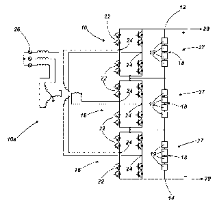
A voltage source converter 10a according to a first embodiment
of the invention is shown in Figure 1.
The voltage source converter 10a comprises first and second DC
terminals 12,14, three phase elements 16 and three auxiliary converters 18.
In use, the first and second DC terminals 12,14 are respectively
connected to positive and negative terminals of a DC network 20, the positive
and
negative terminals respectively carrying a voltage of +VDc/2 and -VDc/2, where
VDc is the voltage range of the DC network 20.
Each of the three phase elements 16 includes two parallel-
connected pairs of series-connected primary switching elements 22. Each
primary
switching element 22 is in the form of one or more series-connected insulated
gate
bipolar transistors, each insulated gate bipolar transistor being connected in
parallel with an anti-parallel diode. The mid-points between each string of
series-
connected primary switching elements 22 define AC terminals 24 for connection
in use to a respective phase of a three-phase AC network 26.
CA 02795315 2012-10-03
WO 2011/127980
PCT/EP2010/054974
In use, the primary switching elements 22 are controllable to
facilitate power conversion between the AC and DC networks 26,20. For
example, the primary switching elements 22 may be controlled to switch on and
off once every cycle of the frequency of the AC network 26 to enable
conversion
5 of a DC voltage presented to the DC side of the respective phase element
16 to an
AC voltage.
Each auxiliary converter 18 is in the form of a chain-link
converter including a chain of modules 19 connected in series, and is
connected in
parallel with a respective one of the phase elements 16 to define a single-
phase
1 o converter limb 27. The three single-phase converter limbs 27 are
connected in
series on the DC side of the circuit between the first and second DC terminals
12,14 to define a two-terminal DC network for three-phase power transmission
The phase elements 16 and auxiliary converters 18 of each
single-phase converter limb 27 operate independently of the other single-phase
converter limbs 27, and therefore only directly affect the phase connected to
the
AC terminals 24 of the respective phase element 16, and have limited influence
on
the phases connected to the AC terminals 24 of the other phase elements 16.
In use, operation of the voltage source converter 10a results in
the presentation of a first DC voltage to the DC network 20 in which the first
DC
voltage is equal to the sum of the individual DC voltages across the phase
elements 16.
In embodiments of the invention, each module 19 of each chain-
link converter 18 may include a pair of secondary switching elements connected
in
parallel with a capacitor in a half-bridge arrangement to define a 2-quadrant
unipolar module that can provide zero or positive voltage and can conduct
current
in two directions
In other embodiments, each module 19 of each chain-link
converter 18 may include two pairs of secondary switching elements connected
in
parallel with a capacitor in a full-bridge arrangement to define a 4-quadrant
bipolar
module that can provide negative, zero or positive voltage and can conduct
current
in two directions.
CA 02795315 2012-10-03
11
WO 2011/127980
PCT/EP2010/054974
The secondary switching elements of each module 19 are
operable so that the chain of modules 19 provides a stepped variable voltage
source.
Each secondary switching element includes an insulated gate
bipolar transistor connected in parallel with an anti-parallel diode.
The fast switching capabilities of insulated gate bipolar
transistors allow the or each auxiliary converter 18 to not only synthesize
complex
waveforms to modify the first DC voltage, but also to synthesize high quality
waveforms to further minimise harmonic distortion and DC ripple levels.
1 o Furthermore the inclusion of such semiconductor devices allows the
auxiliary
converters 18 to respond quickly to changes in the AC and DC voltages and
alter
the characteristics of the synthesised waveforms accordingly.
It is envisaged that in other embodiments of the invention each
of the primary and secondary switching elements may include a different
semiconductor device such as a field effect transistor, a gate turn-off
thyristor, a
gate commutated thyristor, an integrated gate commutated thyristor, a
transistor or
other forced commutated or self commutated semiconductor switches,
accompanied by a reverse-parallel connected diode.
It is also envisaged that in other embodiments each of the
primary and secondary switching elements may include a single semiconductor
device or a string of semiconductor devices connected in series. The series
arrangement allows the use of semiconductor devices with low power ratings
provides a combined power rating that is compatible with the high voltage
nature
of power transmission.
In further embodiments, it is envisaged that the capacitor of each
of the modules 19 may be replaced by a different energy storage device such as
a
fuel cell, a battery, photovoltaic cell or an auxiliary AC generator with an
associated rectifier.
The capacitor of each module 19 may be bypassed or inserted
into the chain-link converter 18 by changing the state of the secondary
switching
elements.
CA 02795315 2012-10-03
12
WO 2011/127980
PCT/EP2010/054974
A capacitor of a module 19 is bypassed when a pair of secondary
switching elements is configured to form a short circuit in the module 19,
causing
the current in the voltage source converter 10a to pass through the short
circuit and
bypass the capacitor.
A capacitor of a module 19 is inserted into the chain-link
converter 18 when a pair of secondary switching elements is configured to
allow
the converter current to flow into and out of the capacitor, which is then
able to
charge or to discharge its stored energy and provide a voltage. In embodiments
employing the use of 4-quadrant bipolar modules, the secondary switching
elements may be configured to insert the capacitor in forward or reverse
directions
so as to provide a positive or negative voltage.
It is therefore possible to build up a combined voltage across the
chain-link converter 18, which is higher than the voltage available from each
of
the individual modules 19 via the insertion of the capacitors of multiple
modules
19, each providing its own voltage, into the chain-link converter 18.
The ability of a 4-quadrant bipolar module to provide positive or
negative voltages means that the voltage across each chain-link converter 18
may
be built up from a combination of modules 19 providing positive or negative
voltages. The energy levels in the individual capacitors may be maintained
therefore at optimal levels by controlling the modules 19 to alternate between
providing positive or negative voltage.
It is also possible to vary the timing of switching operations for
each module 19 such that the insertion and/or bypass of the capacitors of
individual modules 19 in the chain-link converter 18 results in the generation
of a
voltage waveform. An example of a voltage waveform generated using the chain-
link converter 18 is shown in Figure 2, in which the insertion of the
capacitors of
the individual modules 19 is staggered to generate a 50Hz sinusoidal waveform.
Other waveform shapes may be generated by adjusting the timing of switching
operations for each module 19 in the chain-link converter 18.
CA 02795315 2012-10-03
13
WO 2011/127980
PCT/EP2010/054974
It is envisaged that in other embodiments, each chain-link
converter 18 may be replaced by other power converter arrangements with
similar
waveform synthesis capabilities.
In use, each auxiliary converter 18 may be used to modify a
second DC voltage presented to the DC side of the respective phase element 16
by
synthesizing a near-approximation of a rectified sinusoidal waveform for
presentation to the DC side of the phase element 16. This results in the
production
of a near-perfect sine-wave, with minimal harmonic distortion, on the AC side
of
the phase element 16. The voltage source converter 10a does not therefore
require
harmonic filters on the AC side of the converter 10a to control power quality.
This also allows the primary switching elements 22 to be
switched at near zero voltage and therefore results in almost zero switching
losses
during normal operation of the converter.
The use of auxiliary converters 18 means that the voltage profile
presented to the primary switching elements 22 of each phase element 16 is
imposed and controlled by the respective auxiliary converter 18, and is a
slowly
changing waveform rather than the high voltage steps that would otherwise be
presented to the insulated-gate bipolar transistors. It therefore removes the
need for
complex active gate drives and large voltage sharing components within the
main
converter design, and instead results in simpler, less expensive and more
efficient
hardware.
In addition, the use of the auxiliary converters 18 enables the
voltage imposed on the primary switching elements 22 of each phase element 16
to
be rapidly ramped to zero (or minimum value) when required, during fault
conditions, to facilitate soft switching at reduced voltage.
In order to compensate for changes in the real power and/or
reactive power requirements on the AC side of the phase element 16, the
auxiliary
converter 18 is preferably operable to synthesize a waveform including a
triplen
harmonic voltage to modify the first DC voltage. This results in the
production of a
compensatory DC voltage component to compensate for the resultant change in
the
DC voltage on the DC side of the phase element 16.
CA 02795315 2012-10-03
14
WO 2011/127980
PCT/EP2010/054974
For example, in circumstances where it becomes necessary to
generate reactive power on the AC side of the phase element 16, the auxiliary
converter 18 is operable to synthesize a waveform including a rectified, zero-
phase
sequence triplen harmonic component. This results in the production of a
negative
compensatory DC voltage component to compensate for the resultant increase in
the first DC voltage.
In circumstances where it becomes necessary to absorb reactive
power from the AC side of the phase, the auxiliary converter 18 is operable to
synthesize a waveform including a rectified, zero-phase sequence triplen
harmonic
component. This results in the production of a positive compensatory DC
voltage
component to compensate for the resultant decrease in the first DC voltage.
By controlling each auxiliary converter 18, it is possible to
produce a compensatory DC voltage component so as to ensure that the net
increase or decrease in the first DC voltage is controlled to be zero whilst
the AC
voltage can be made to vary in order to allow reactive power control.
Operation of each auxiliary converter 18 to synthesize
waveforms including rectified triplen harmonic components may also be used to
increase the AC voltage on the AC side of the phase element 16 in
circumstances
where the reactive power requirement is small or not needed.
This reduces the current drawn by the converter 10a for a given
power conversion in both rectified and inverter operating modes. This is
beneficial
because lower levels of current flow reduce power losses that would otherwise
occur in converter equipment. It may also reduce the ripple current components
in
any capacitors (not shown) connected to the DC side of the phase element 16,
thereby reducing capacitance requirements and associated power losses.
Zero-phase sequence, 3rd harmonic components are not seen in
the primary line to line voltage waveforms or in the primary or secondary side
current waveforms. Other triplen waveforms (e.g. 9th, 15th 21st,
etc.) may also be
applied with similar effects.
The zero-phase sequence nature of the rectified triplen harmonic
components means that when a transformer is used to interconnect the voltage
CA 02795315 2012-10-03
WO 2011/127980
PCT/EP2010/054974
source converter 10a and the AC network 26, the effects of the additional
modulation is limited to the secondary side of the transformer connected to
the
voltage source converter 10a and has no effect on the AC line voltage and
current
at the primary side of the transformer connected to the AC network 26.
5 However,
the addition of rectified triplen harmonic components
to the synthesized waveforms results in DC ripple in the first DC voltage. For
example, addition of 3rd harmonic components results in DC ripple components
appearing in the first DC voltage, which are in the form of 6th, 12th, 18th
etc
harmonics of the AC supply frequency
1 o To
minimise the DC ripple arising from the addition of rectified
triplen harmonic components, each auxiliary converter 18 is operable to
synthesize
a waveform including at least one rectified, zero-phase sequence triplen
harmonic
component.
The inclusion of one or more rectified zero-phase sequence
15 triplen harmonic components in each synthesized waveform results in the
elimination of one or more of the harmonic ripple components in the first DC
voltage. For example, when the DC ripple in the first DC voltage includes 6th
and
12th harmonic ripple components, the inclusion of 9th and 15th zero-phase
sequence
harmonic components in each of the synthesized waveforms will result in the
cancellation of the 6th and 12th harmonic ripple components and thereby
minimise
DC ripple in the first DC voltage.
Figure 3 shows the ratio of the first DC voltage to fundamental
component of AC side voltage required to facilitate reactive power control for
a
voltage source converter and the required amount of 3rd harmonic modulation 28
in the presence of a constant average DC side voltage. Also shown are the
corresponding relative levels of 9th and 15th harmonic modulation 30,32
required to
totally eliminate the 6th and 12th harmonic ripple components from the summed
voltage appearing at the DC network as a result of the 3rd harmonic
modulation.
An example of a synthesized waveform is shown in Figure 4, in which, for an
operating condition near to 0.8 modulation index, the synthesized waveform 34
CA 02795315 2012-10-03
16
WO 2011/127980
PCT/EP2010/054974
and the corresponding AC side waveform 36 includes 3th, 9th and 15th harmonic
components.
As outlined above, the introduction of zero-phase sequence
triplen harmonic components into the synthesized waveforms has minimal effect
on the AC network.
Another approach to minimise DC ripple in the first DC voltage
is shown in Figure 5.
In this approach, each auxiliary converter 18 may be controlled
in use to synthesize a waveform 38 including a DC voltage component and a
second harmonic AC voltage component, each synthesized waveform 38 operating
at phase difference of 120 electrical degrees to the other two synthesized
waveforms 38. The summation of these three synthesized waveforms 38 leads to
the second harmonic AC voltage components cancelling out each other and
thereby results in a ripple-free DC side voltage 40 consisting of the DC
voltage
components at the DC network 20. In other embodiments, each synthesized
waveform 38 may include more than one harmonic AC voltage component.
Such waveforms are more straightforward to synthesize, which
simplifies control of each auxiliary converter 18 when synthesizing the
waveform.
Each of the synthesised waveforms 38 is also presented to the
DC side of the respective phase element 16. The presence of non zero-phase
sequence harmonic AC voltage components in the synthesized waveforms results
in an AC side waveform 42 with low levels of harmonic distortion at the AC
network 26.
To eliminate the harmonic distortion caused by the presence of
non zero-phase sequence harmonic AC voltage components, the voltage source
converter may further include the use of tertiary converters.
Each single-phase converter limb 27 of the voltage source
converter 10a shown in Figure 1 may be modified to include one or two tertiary
converters 44, each tertiary converter being connected on either side of the
phase
element 16 to define a series connection, as shown in Figure 6. Each tertiary
converter 44 of each single-phase converter limb 27 operates independently of
that
CA 02795315 2012-10-03
17
WO 2011/127980
PCT/EP2010/054974
of the other single-phase converter limbs 27 and therefore only directly
affects the
phase connected to the AC terminals 24 of the respective phase element 16, and
has limited influence on the phases connected to the AC terminals 24 of the
other
phase elements 16.
Each tertiary converter 44 is in the form of a chain-link converter
including a chain of modules 45 connected in series, which is operable in a
similar
manner to the chain-link converter 18 described above with reference to Figure
1.
As outlined above, the structure of the chain-link converter allows the
synthesis of
a near-approximation of a rectified sinusoidal waveform for presentation to
the DC
side of the respective phase element 16, and thereby allows the second DC
voltage
to have a different form to that of the waveform synthesized by the auxiliary
converter 18.
The use of the tertiary converters 44 in this manner leads to the
generation of an AC sinusoidal waveform 42, with minimal harmonic distortion,
on the AC side of the phase element 16 and thereby minimises the
aforementioned
effects of non zero-phase sequence harmonic AC voltage components on the AC
network when each auxiliary converter 18 is controlled in use to synthesize a
waveform 38 including a DC voltage component and at least one harmonic AC
voltage component to minimise DC ripple in the first DC voltage.
A voltage source converter 10b according to a second
embodiment of the invention is shown in Figure 7.
The voltage source converter 10b in Figure 7 is similar to the
voltage source converter 10a in Figure 1 except that the phase elements 16 are
connected in a cascade arrangement to define a first limb 46, three auxiliary
converters 18 are connected in a cascade arrangement to define a second limb
48,
the first and second limbs 46,48 being connected in parallel on the DC side of
the
circuit between the first and second DC terminals 12,14, and each tertiary
converter 44 is connected between a respective one of the junctions between
the
phase elements 16 and a respective one of the junctions between the auxiliary
converters 18.
CA 02795315 2012-10-03
18
WO 2011/127980
PCT/EP2010/054974
This converter arrangement is advantageous in that each tertiary
converter 44 is operable in use to modify a plurality of second DC voltages,
each
second DC voltage being presented to the DC side of the respective phase
element
16 instead of assigning a tertiary converter 44 to a respective phase element
16.
The reduced number of tertiary converters 44 results in a reduction in
hardware
size, weight and costs.
The inclusion of auxiliary and/or tertiary converters in the
converter arrangement therefore provides the voltage source converter with DC
side active filtering capability for minimising DC ripple, and thereby
eliminates
1 o the need for DC side filtering equipment in the form of passive
inductive and
capacitive elements. This leads to reductions in converter hardware costs,
size and
weight whilst increasing the reliability and efficiency of the associated
power
station.