Note: Descriptions are shown in the official language in which they were submitted.
CA 02796985 2012-10-19
WO 2011/134057
PCT/CA2011/000475
POWER CONVERTER FOR A POWER GENERATOR
Field
This invention relates to circuits, systems, and methods for converting power
obtained
from a power generator. The circuits, systems, and methods described herein
may be used to
interface a power generator to a power distribution grid.
Background
Grid-connected power generation systems typically include two major parts:
power
generators that produce the power and converters that receive, condition, and
inject the power
into the power distribution grid. Power generators include, for example,
photovoltaic (PV)
cells, fuel cells, and wind turbines.
To increase the overall efficiency of power generators under different
circumstances,
such as partial shadowing of PV cells, or mismatches between PV cells or wind
turbines,
independent control and power extraction is required for each power generator.
This requires
using a separate converter for each power generator. This may be referred to
as micro-
inverter technology.
In single-phase grid-connected power generation systems, the instantaneous
output
power oscillates at twice the grid frequency. In systems where the power
generators are PV
cells, the input power generation is DC and thus oscillation of the
instantaneous power at the
converter output, if reflected in the input, causes the input operating point
to deviate from
- 1 -
CA 02796985 2012-10-19
WO 2011/134057
PCT/CA2011/000475
DC. If there is any power oscillation on the PV cell side, maximum power is
only achievable
at the peak of oscillation, which translates into less average power
extraction than the
available maximum power [1,2]. This is a power loss that reduces the
efficiency of the PV
cell system. Therefore, power pulsation is a key problem in such systems and
the PV cell
converter should decouple the output power pulsation from the input DC power
generation to
maximize the efficiency.
As noted above, if there is no power decoupling in a single-phase inverter,
the power
generation at the PV cell terminal will contain oscillations that result in a
deviation from the
optimum point. Energy storage in the circuit may supply oscillatory power and
reduce power
pulsation at the PV cell terminal. The decoupling problem is normally resolved
by using
large electrolytic capacitors (e.g., in the range of milli-Farads) to minimize
the effect of the
output power pulsation on the input operating point. However, this is highly
undesirable
because it decreases the life-time and increases the volume, weight, and cost
of the inverter.
Depending on the topology, different locations of the energy storage are
possible. For
example, for a single-stage topology energy storage may be implemented at the
PV cell
terminals. For multi-stage topologies, when a voltage source inverter is
employed at the
output, the power decoupling capacitor may be placed at the input terminals
and/or at the DC
bus (e.g., between DC-DC converter and DC-AC inverter stages). It is
beneficial to have
most of the decoupling capacitance on the DC bus because the voltage level is
higher and the
same amount of energy storage can be achieved with a smaller capacitor.
The generation of a high DC voltage is not efficient and it poses an excessive
voltage
stress on the inverter and on the output of the first stage. Moreover, the
high voltage on the
bus enlarges high frequency ripples on the output current, which requires
large passive filters
for compensation. Further, in such an approach relatively large electrolytic
capacitors at the
input are still needed to remove any oscillations at the PV cell input.
Use of a voltage source inverter at the output requires a bulky inductor for
connection
to the grid. To avoid this, a micro-inverter may use an unfolding power
circuit in the last
stage. However, with this approach, a large electrolytic capacitor bank is
still required at the
PV cell terminals because the voltage level is very low and the amount of
capacitance
required becomes large. In general, topologies that use a transformer as an
energy buffer
employ such a configuration for power decoupling [1,2,5].
- 2 -
CA 02796985 2012-10-19
WO 2011/134057
PCT/CA2011/000475
To reduce the amount of input capacitance required, a multistage approach may
be
used as in [3] which processes the full output power. However, this reduces
the efficiency
and increases the size and weight of the converter. Moreover, since the DC bus
voltage is
very high the stress on the switches of the converter stages is very high and
also the filter that
shapes the current becomes relatively large.
In other approaches [5-10], an auxiliary power circuit is introduced that
absorbs
power and provides energy when needed. As a result a large electrolytic
capacitor is not
required. The auxiliary power circuit usually operates at high voltage to
reduce the energy
storage component. Such approaches generally have low efficiency and have high
number of
power processing stages.
Summary
Described herein is a power converter for use with a power generator,
comprising: a
high side input point and a low side input point for receiving substantially
DC power from the
power generator; a capacitor connected across the high side and low side input
points; a first
means that receives voltage across the capacitor and converts the voltage into
a high
frequency AC voltage while rejecting or minimizing oscillations in the
received voltage; a
second means that converts the high frequency AC voltage into a substantially
sinusoidal AC
voltage or current; an isolating transformer that receives the substantially
sinusoidal AC
voltage or current; a third means that converts a high frequency substantially
sinusoidal AC
voltage or current from the transformer into (i) a low frequency substantially
sinusoidal AC
output voltage or current; and (ii) a DC output voltage or current; and a high
side output point
and a low side output point for outputting the output voltage or current.
In one embodiment the high frequency AC voltage may be amplitude modulated by
a
substantially sinusoidal voltage at a frequency that is related to a power
distribution grid
frequency.
The first means may comprise a chopper circuit. Switches of the chopper
circuit may
be controlled using pulse width modulation. The second means may comprise a
resonant
circuit. The resonant circuit may be a series resonant circuit. The third
means may comprise
a rectifier and optional filter, wherein the output is a DC voltage or
current. The third means
may comprise a rectifier and an inverter, wherein the output is an AC voltage
or current.
- 3 -
CA 02796985 2012-10-19
WO 2011/134057
PCT/CA2011/000475
Also described herein is a micro-inverter for a distributed power generator,
comprising: the power converter described above; and a controller that
controls operation of
switches in the first means by comparing the voltage across the capacitor with
a reference
voltage so as to minimize voltage fluctuations across the capacitor. The
controller may
include one or more of a modified pulse width modulator, a duty cycle
controller, and a
maximum power point tracker. The duty cycle controller may comprise a
proportional
integral-derivative compensator.
Also described herein is a power generation system, comprising: at least one
micro-
inverter as described above; and at least one power generator. Each power
generator may be
connected to a micro-inverter.
Also described herein is a method for obtaining power from a power generator,
comprising: converting substantially DC output power from the power generator
into a high
frequency AC voltage while rejecting or minimizing oscillations in the output
power from the
power generator; converting the high frequency AC voltage into a high
frequency
substantially sinusoidal voltage or current; and converting the high frequency
substantially
sinusoidal AC voltage or current into (i) a DC voltage or current, and (ii) a
low frequency
substantially sinusoidal AC voltage or current; wherein the high frequency
substantially
sinusoidal AC voltage or current is isolated from the DC voltage or current or
the low
frequency substantially sinusoidal AC voltage or current.
In one embodiment the method may include amplitude modulating the high
frequency
AC voltage by a substantially sinusoidal voltage at a frequency that is
related to a power
distribution grid frequency.
The method may comprise using a chopper to convert output power from the power
generator into a high frequency AC voltage. The method may comprise using
pulse width
modulation to control one or more switches of the chopper circuit. The method
may include
comparing output voltage of the power generator with a reference voltage so as
to minimize
voltage fluctuations of the power generator. The method may comprise using a
resonant
circuit to convert the high frequency AC voltage into a high frequency
substantially
sinusoidal AC voltage or current. The resonant circuit may comprise a series
resonant circuit.
The method may comprise connecting the low frequency substantially sinusoidal
output
voltage or current to a power distribution grid.
- 4 -
CA 02796985 2012-10-19
WO 2011/134057
PCT/CA2011/000475
In the above circuits, systems, and methods, the power generator may be a
photovoltaic (PV) cell or a fuel cell.
Brief Description of the Drawings
For a better understanding of the invention, and to show more clearly how it
may be
carried into effect, embodiments will now be described, by way of example,
with reference to
the accompanying drawings, wherein:
Figure 1 is a generalized block diagram of a micro-inverter.
Figure 2 is a block diagram of a micro-inverter according to one embodiment.
Figure 3(a) is a circuit diagram of a micro-inverter with maximum power point
tracking according to one embodiment.
Figure 3(b) is a circuit diagram of a micro-inverter with maximum power point
tracking according to another embodiment.
Figure 3(c) is a plot showing operating waveforms of the circuit of Figure
3(b).
Figure 4(a) is a plot showing typical current-voltage and power-voltage
characteristics
and the maximum power point of a PV cell, and Figure 4(b) is a plot showing
how the
characteristics change with amount of irradiation.
Figure 5 is a plot showing typical steady-state operating waveforms of the
embodiment of Figure 2.
Figures 6(a) to (f) show schematic diagrams of equivalent circuits of the
embodiment
of Figure 3(a), for each interval of the plot of Figure 5.
Figure 7 is a circuit diagram showing the kth harmonic equivalent circuit of
the circuit
in Figure 2.
Figures 8(a) and (b) are plots showing zero voltage switching of the switches
M1 (a)
and M2 (b) of Figure 3(a), obtained from a simulation.
Figure 9 is a plot showing the bus and grid voltage waveforms and the gate
signals for
the embodiment of Figure 3(a) using modified pulse width modulation as
described herein.
- 5 -
CA 02796985 2012-10-19
WO 2011/134057
PCT/CA2011/000475
Figure 10 is a plot showing output grid current waveform with conventional
pulse
width modulation and with modified pulse width modulation.
Figure 11 is a plot showing zero voltage switching of a simulation based on
the circuit
of Figure 3(a).
Figure 12 is a plot showing bus voltage and resonant tank current and voltage
of a
simulation based on the circuit of Figure 3(a).
Detailed Description of Embodiments
Described herein are systems, circuits, and methods for obtaining power from a
power
generator. A power generator may be, for example, a wind turbine, a fuel cell,
or a
photovoltaic cell. The power generator may be a distributed power generator.
Whereas
embodiments of the systems, circuits, and methods are described herein
primarily with
respect to photovoltaic cells, it will be appreciated that the systems,
circuits, and methods are
not limited thereto.
The systems, circuits, and methods described herein may be used in a micro-
inverter
for a power generator. As used herein, the term "micro-inverter" refers to a
device that
interfaces a power generator with a load, such as a power distribution grid. A
system
including a micro-inverter is shown in the generalized block diagram of Figure
1. The micro-
inverter 20 receives power from a power generator 10, and outputs power to a
load 30. The
micro-inverter 20 may include a power section 200 that may include one or more
stages and
perform one or more functions, such as, for example, DC-DC conversion, DC-AC
conversion, or a combination thereof. The micro-inverter may include a control
section 300
that may perform one or more functions such as, for example, maximum power
point tracking
of the power generator, and/or providing gating signals to the power section
200. The gating
signals may be determined by sensing the power generator voltage and/or
current, and/or the
load voltage and/or current.
A micro-inverter as described herein increases the overall efficiency of power
generation under different circumstances and conditions. For example, in the
case of a PV
cell, partial shadowing of the PV cell or mismatches between PV cells can
degrade the
overall efficiency of the system. However, use of a micro-inverter for each PV
cell, or for a
- 6 -
CA 02796985 2012-10-19
WO 2011/134057
PCT/CA2011/000475
PV cell string or module, permits independent control and power extraction
from each PV
cell or PV cell string or module, maximizing power extraction from PV cells
despite varying
conditions of individual PV cells.
A micro-inverter as described herein is compact, so as to be attached to a PV
cell
(e.g., to the back of a PV cell). Since micro-inverters are exposed to a wide
range of
environmental conditions, such as extremes of temperature and humidity,
reliability and
maintenance of are major issues. This exposure also adversely affects the life
expectancy and
performance of the inverter. These factors demand robust design and
construction, and may
require more expensive components that lead to a higher manufacturing cost.
Consequently,
challenges in the design of a micro-inverter include achieving compactness and
low cost, e.g.,
by reducing the number and size of circuit components. Advantageously, a micro-
inverter as
described herein does not require costly high voltage components and wiring.
In one embodiment, a micro-inverter may include one or more feature such as,
for
example, communication, inversion (i.e., DC to AC conversion), peak power
tracking,
islanding, etc. Such a micro-inverter may be integrated into a PV module. The
term "PV
module" refers to one or more PV cells connected in series, parallel, and/or
series-parallel to
effect a desired electrical output. For example, a PV module may be the
smallest discrete
unit provided (e.g., sold) to an end user of a photovoltaic conversion system.
Typically, PV
modules are supplied with connectors or other suitable hardware to extract the
DC output
from the module. However, as described herein, a micro-inverter may be
integrated into a
PV module, wherein such connectors or other suitable hardware to extract the
DC output are
replaced with a micro-inverter so as to obtain one or more electrical
features, such as those
described above. Moreover, such integration of the micro-inverter with the PV
module may
include packaging of the micro-inverter either substantially together or
incorporated into the
module packaging, or in a manner that substantially unifies the micro-inverter
with the
module packaging. The PV module packaging may be pre-existing or may be
designed to
accommodate the micro-inverter. It will be appreciated that the inversion
portion of the
micro-inverter may be of any design, such as, for example, but not limited to,
current source,
voltage source, resonant, etc., and may include single or multiple power
stages.
The control section 300 of a micro-inverter as described herein may include
maximum power point tracking (MPPT). As a result, MPPT may be performed on
each
power generator independently. In the case of PV cells, this is useful where
partial shading
- 7 -
CA 02796985 2012-10-19
WO 2011/134057
PCT/CA2011/000475
cannot be avoided since MPPT allows the maximum power to be extracted from
each PV cell
for any instantaneous condition. MPPT removes any mismatch losses between PV
cells in
the system. Further, micro-inverters as described herein provide modularity to
individual
power generators, allowing a "plug and play" approach to their use in a
distributed power
generation system. The control section may be implemented in whole or in part
using
discrete components, using digital technology (e.g., in a digital signal
processor (DSP), field
programmable gate array (FPGA), or application specific integrated circuit
(ASIC) device),
or using a combination thereof. For example, one or more components of the
control section
may be implemented in an algorithm using a suitable hardware language such as,
for
example, very high speed integrated circuit (VHSIC) hardware descriptive
language (VHDL),
register transfer language (RTL), or Verilog. Such an algorithm may be
implemented in, for
example, a FPGA or ASIC device, or other suitable logic device. Use of digital
technology
provides a controller that is compact and robust.
As used herein, the terms "maximum power point tracking (MPPT)" and "maximum
power point tracker (MPP tracker)" are distinct. "MPPT" refers to an algorithm
and "MPP
tracker" refers to hardware (i.e., a circuit). The MPPT calculates the optimum
operating
point for a distributed power generator such as a photovoltaic cell, and
provides a reference
point for MPP tracker to steer the system toward the optimum operating point.
As used herein, the term "photovoltaic cell (PV cell)" refers to any cell
having a light
absorbing material to absorb photons and generate electrons via a
photoelectric effect. A
non-limiting example of a photovoltaic cell is a solar cell. The light
absorbing material may
absorb light in any wavelength or combination of wavelengths, including, for
example,
wavelengths of solar light that reach the earth's surface, and/or wavelengths
of solar light
beyond the earth's atmosphere. Two or more light absorbing materials having
specific
wavelengths of light absorption may be used in combination to take advantage
of different
light absorption and charge separation mechanisms. The light absorbing
material may be
configured as, for example, bulk material, thin-film (e.g., inorganic layers,
organic dyes, and
organic polymers), and/or nanocrystals. Photovoltaic cells may be combined
into arrays,
strings, modules, or panels. For example, a photovoltaic cell string may
include a plurality of
photovoltaic cells connected together in a series, parallel, series-parallel,
or other
configuration. For simplicity, the term "PV cell" as used herein will refer to
a single cell or
any such combination of cells.
- 8 -
CA 02796985 2012-10-19
WO 2011/134057
PCT/CA2011/000475
A review of existing micro-inverter topologies reveals that for power
decoupling,
electrolytic capacitors, very high bus voltage, or auxiliary power circuits
are used. The
former has life-time, size, and maintenance problems and the latter approaches
mainly exhibit
low efficiency, high number of stages, and/or high voltage stress which
compromise
performance.
A micro-inverter topology as described herein overcomes the aforementioned
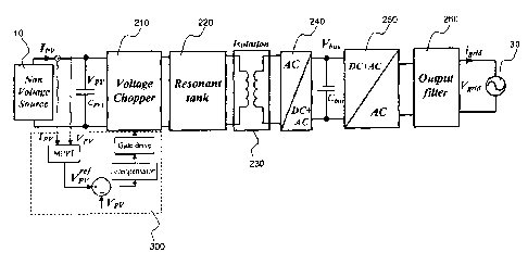
problems. Figure 2 shows a block diagram of an embodiment of the power circuit
200
together with a control section 300. Referring to Figure 2, a capacitor Cpvi
is connected
across the power generator 10 and the input of a voltage chopper 210. The
voltage chopper
topology may be, for example, half bridge or full bridge. From the voltage
chopper, the
circuit includes a resonant tank circuit 220, an isolation transformer 230, a
first converter
240, a capacitor Cbus, a second converter 250, and an output filter 260. The
converters may
be voltage source converters. A half bridge or full bridge rectifier may be
provided at the
output of the isolation transformer. The control section 300 provides gate
signals for the
voltage chopper 210 and may also provide maximum power point tracking. The
control
section also provides decoupling and high switching frequency of the voltage
chopper stage
210, to ensure that main power pulsations are drawn from the bus capacitor
Cbus and input
power extraction is constant, while using only a small capacitor Cpvi at the
PV terminal. The
decoupling method creates a DC plus AC voltage at the middle stage converter
240 and then
uses a modified pulse width modulation (PWM) technique to remove double
frequency
harmonics from the output current. Therefore, the power pulsations have
minimum impact
on the input power extraction or output power injection. By accepting a large
AC oscillation
on the bus and controlling the average bus voltage, both the value of the bus
capacitor and the
voltage stress on the inverter may be optimized. For example, the input and
bus capacitors
may be reduced to less than 20 microFarad, an improvement of two or three
orders of
magnitude, relative to prior designs. As a result, the topology and control
systems described
herein yield a compact design suitable for micro-inverter application.
A micro-inverter as described herein employs an isolated resonant-mode
topology
using a high switching frequency. The high switching frequency (e.g., 10 kHz
or higher)
allows use of small circuit components, relative to a lower switching
frequency, resulting in a
high power density. In general, as the switching frequency increases,
switching losses
associated with turning on and off the active device(s) also increase,
typically resulting in low
conversion efficiency. However, in the embodiments described herein, the high
switching
- 9 -
CA 02796985 2012-10-19
WO 2011/134057
PCT/CA2011/000475
frequency does not affect the efficiency of the circuit because a soft
switching technique is
employed. Soft switching refers to the switching of a device (i.e., turning
the device on or
off) when there is zero voltage across the device (i.e., zero voltage
switching (ZVS)) or zero
current through the device (i.e., zero current switching (ZCS)). That is, in a
resonant-mode
topology the switching losses are low, allowing operation of a resonant
converter at a high
switching frequency with low switching loss.
In one embodiment the isolated resonant-mode converter is a series resonant
converter. This embodiment exhibits near zero switching losses while operating
at constant
and very high frequencies (e.g., 100 kHz or higher). The component count is
low, making it
feasible for micro-inverter applications.
The embodiment of Figure 2 is suitable for obtaining power from a power
generator
and interfacing the power with an AC load, such as a power distribution
system. Figure 3(a)
shows an exemplary circuit diagram of an embodiment without a converter stage
250 (see
Figure 2), but with a load RL, wherein the output may be DC. This embodiment
also employs
a series resonant DC-DC converter. As shown in Figure 3(a), the embodiment may
include a
control section 300, wherein maximum power point tracking (MPPT) may be
employed. The
power generator 10 may be a PV cell. The circuit includes a chopper (M1, M2,
shown with
their body diodes Dmi and Dm2), a series resonant tank (Cs, Ls), a high
frequency isolation
transformer (T), a rectifying circuit (D1, D2) and an output filter (Cf). The
function of the
chopper is to convert the DC input voltage (Vg) to a high frequency AC
voltage. The series
resonant tank converts this AC voltage into oscillatory (i.e., substantially
sinusoidal) current
(i), with low frequency voltage components. This feature is useful, when, for
example, the
load is an inverter which is injecting the power into a power distribution
grid. Low frequency
ripple generated by the inverter may be substantially blocked by the resonant
tank, preventing
it from appearing at the input and allowing use of small energy-storage
capacitors. The high
frequency transformer provides matching and isolation for the output voltage.
The rectifying
circuit and the output filter convert the high frequency resonant current into
a DC output
voltage. The load RL may be a DC load, a converter stage, or a converter
and/or inverter
stage, as shown in Figure 2. For example, the load may be an inverter that
produces AC
output power suitable for injection into a power distribution grid.
As used herein, the term "low frequency" refers to a harmonic frequency that
is
derived from the AC grid frequency.
- 10 -
CA 02796985 2012-10-19
WO 2011/134057
PCT/CA2011/000475
As used herein, the term "high frequency" refers to a switching frequency of
the
converter and one or more harmonics thereof
An alternative embodiment is shown in Figure 3(b). This embodiment is based on
a
full bridge resonant converter with a series resonant tank. The full bridge
may be controlled
using a modified phase shift modulation technique. Soft switching of the power
MOSFET
switches MI-Ma may be achieved by tuning the resonant frequency of the series
resonant tank
circuit Cs-Ls lower than the operation frequency of the resonant inverter.
This is an inductive
mode where the impedance viewed from the input port of the resonant tank 4,
becomes
inductive. Resonant current lags the fundamental voltage and as a result 0
becomes positive.
Switches M1 and M3 turn on during negative current, therefore, they have zero
voltage turn
on because current always transfers from the anti-parallel diode to the
MOSFET. The
scenario is the same for switches M2 and Mg. All the switches turn off under
non-zero
resonant current. Snubber capacitors may be used to reduce turn-off switching
losses.
Principle operating waveforms of the embodiment of Figure 3(b) are shown in
Figure
3(c). The output voltage of the converter (vab) is regulated through the
change of the phase
shift a between the two pulses for M1 and M3 in Figure 3(c). The phase shift
angle increases
when the input capacitor voltage decreases, and the phase shift angle
decreases when the
input capacitor voltage increases. In this manner, regardless of the output
load (RL)
stipulated by the next stage, or environmental conditions for the PV module,
the input voltage
can be regulated to remove, reduce, or minimize oscillations from the input
port and to
substantially avoid deviation from the maximum power point.
The embodiment of Figures 2 and 3(a) will now be described in detail. The
inverter
output current controller forces the current to be in-phase with the grid
voltage. Since the
input power extraction from the power generator is DC, the power oscillation
will be drawn
from the bus capacitor Cbus and the resonant tank passive elements. As a
result the passive
components may be small. With some simplification, bus voltage oscillation may
be derived
as follows:
AVbn = ________________________________________
=VD'
"Ig s bus ( 1 )
This equation shows that for a given DC bus voltage and input power, if the
bus
voltage variation is large a smaller bus capacitor may be selected. For
example, in a
-11 -
CA 02796985 2012-10-19
WO 2011/134057
PCT/CA2011/000475
conventional approach the bus voltage variation may be 1 volt, whereas in the
embodiments
described herein, the voltage variation may be 20 volts, so the capacitor may
be 20 times
smaller. The bus voltage can be estimated as:
/ PIll
' '
( '14 'C ( t) = ( VIPIISC ) +
)b vs Sin (2Wgt)
Wg CI) ti R (2)
As a result the equivalent resistance of the embodiment may be calculated as:
4,,, ,(t) -2
( (17,1 t))2 ( " ) 8 Pin
=
R(t) = 1 = Tr N = (1/bDu se )2 + S111(2W
gt)
2.1)`)
SRC' 9 Pr n 72 N2 pn, 6'
Wg bu s
(3)
The maximum and minimum of this equation are used in the following discussion
to
estimate maximum and minimum of RL.
Various techniques may be used to control the switches of the chopper. For
example,
a modified pulse-width-modulation (PWM) technique may be used. For example, in
the
embodiment of Figure 3(a), an asymmetrical pulse-width-modulation (APWM)
technique is
shown. A PV cell may be connected directly to the input of the resonant
converter, as shown
in Figure 3(a). A challenge in using PV cells is presented by their nonlinear
current-voltage
(I-V) characteristics, which result in a unique maximum power point (MPP) on
the power-
voltage (P-V) curve, as shown in Figure 4. Therefore, to achieve maximum power
point
tracking ability, the resonant converter can control its input voltage, so
that it can operate at
any point of the PV cell I-V curve, or at least at points near the maximum
power point
(MPP). The output voltage of the resonant converter may be regulated by a grid-
connected
inverter.
An embodiment of an APWM series resonant converter control scheme is shown in
Figure 3(a). This embodiment includes a MPPT block 310 that receives the input
current Ig
and voltage Vg information from voltage and current sensor blocks H and R,
respectively, a
subtractor 320, a duty cycle controller 330, and an APWM modulator 340 that
produces the
gate signals for switches M1 and M2. In one embodiment the duty cycle
controller may
include a proportional integral-derivative (PID) compensator. The MPPT block
generates a
reference voltage (\Tref) which is compared with Vg and the result fed to the
PID compensator.
The PID compensator forces the input voltage to follow the voltage reference
generated by
the MPPT block.
- 12 -
CA 02796985 2012-10-19
WO 2011/134057
PCT/CA2011/000475
Operation of the series resonant converter of Figure 3(a) will now be
described with
reference to the plot of typical steady state operating waveforms shown in
Figure 5, and the
equivalent circuits shown in Figure 6. The equivalent circuits show the
inherent output
capacitances Cmi and Cm2 of M1 and M2, respectively.
Interval (to-ti): At to, the resonant current i is crossing zero. During this
interval, Mi is
on and M2 is off. The output voltage VAB of the chopper is Vg. Current isc
flows through the
diode D2. The voltage on the primary side of the transformer T is nVo,
neglecting the voltage
drop of the diode. At t, M1 is turned off for voltage regulation.
Interval (t142): At the beginning of this interval, M1 is turned off. The
positive current
flowing through the resonant branch forces the charging of the output
capacitance Cnii of
main switch M1 and the discharging of the output capacitance Cm2 of M2. Once
Cmi has fully
charged and Cõ,2 has fully discharged, the current forces the conduction of
body diode D,,,2 of
M2. At t3, M2 is turned on to achieve zero voltage switching (ZVS).
Interval (t243): During this interval, MI is off and M2 is on. Di is off and
D2 is still on.
The output voltage vAB of the chopper is zero. The voltage on the primary side
of
transformer is nVo. At t3, the resonant current is crossing zero.
Interval (t344): The resonant current changes its direction at t3. It forces
conduction of
the diode Di. During this interval, M2 and DI are on, and Mi and D2 are off
The output
voltage vAB of the chopper is zero. The voltage on the primary side of
transformer also
changes its direction, -nVo. At ta, M2 is turned off
Interval (t445): At the beginning of this interval, M2 is turned off The
negative
current flowing through the resonant branch forces the discharging of the
output capacitance
Cmi of main switch M1 and the charging of the output capacitance Cm2 of M2.
Once Cm' has
fully discharged and Cm2 has fully charged. The current forces the conduction
of body diode
Dmi of Mi. At ts, MI is turned on to achieve zero voltage switching (ZVS).
Interval (t5-to): During this interval, Mi is on and M2 is off D2 is off and
Di is on.
The output voltage vAB of the chopper is Vg. The voltage on the primary side
of transformer
is -nVo. At to, the resonant current i is crossing zero. The current through
the diode DI goes
to zero. Another operating cycle begins.
- 13 -
CA 02796985 2012-10-19
WO 2011/134057 PCT/CA2011/000475
Steady-state analysis
The AC equivalent resistance is given by:
R VP __ (RMS) 8. /12 = R
L
a , = =
1 r(RMS) ar2
(4)
The voltage vAB on the input of the resonant tank: also can be given using
Fourier series:
_
2V = sin(k = D . r)
g ___________________________________________
v ADO) = Dm 'lig + E cos(k = coo =t¨k=D=r)
Ic;---1 kr
_ ¨ (5)
Where coo is the switching frequency and D is the duty cycle. The following
qualities are
defined as:
1
VLs = Cs
CO
0) = ---2-
CO,
QCO, = Ls
0 = ----
lio,
21/., = sin(k = D = ir)
_________________________________ cos(k = r)o=t¨k.D=z)
kr
(6)
The kth harmonic equivalent circuit is shown in Figure 7. The resonant current
ir may be
expressed as:
_
2V = sin(k -D- r)
g cos(k = coo=t¨k=D=g¨ 0 k)
k=1 kr . Zink
_
[ ¨1/2
1
Zink = Ra, = 1+ Q02 = (kco )2
kco
-
9, = arctan Qo = (kw ¨ --1
)
k CO
(7)
- 14-
CA 02796985 2012-10-19
WO 2011/134057
PCT/CA2011/000475
To achieve ZVS for MI, the current at the turn off of M2 must be negative, as
given by (8):
2 V = sin(k = D = 7r)
12= E ________________________ = COS(¨k = D ¨0,)
k=1
1 IJ2
R.,. 1 + Qo2 = (kw ¨ ¨)2
ka)
(8)
To achieve ZVS for M2, the current at the turn off of M1 must be positive, as
given by (9):
2 = V sin(k = D = 7r)
I = E a
= cos(k = D = 7r ¨0k)
k=1 1 ,, h/2
kr = Rac = 1+ Q02 = (kw ____________ 1
40'
(9)
As an example, Figures 8(a) and (b) illustrate zero voltage switching of both
switches,
obtained from a simulation using PSIMTm software version 9 (Powersim Inc.,
Woburn, MA).
Embodiments have been described herein using a voltage input. The embodiments
can also be configured to work with a current input.
Modified Pulse Width Modulation
There may be input power oscillation from the power generator. In such case,
maximum power is only achievable at the peak of oscillation, which translates
into less
average power extraction than the available maximum power. This is a power
loss that
reduces the efficiency of PV systems, and substantially the same problem
exists in systems
with wind turbines or fuel cells as the power generators, for single phase
systems or
unbalanced three phase systems. Therefore, power oscillation is a key problem
in such
systems and the converter should decouple the output power oscillation from
the input DC
power generation to maximize efficiency. Power decoupling is conventionally
performed
passively by using large electrolytic capacitors to minimize the effect of the
output power
oscillation on the input operating point. However, use of large capacitors
increases the size
and weight of the converter, and lowers reliability, resulting in high
maintenance costs.
- 15-
CA 02796985 2012-10-19
WO 2011/134057
PCT/CA2011/000475
The decoupling control method used in the converter described herein removes
double frequency oscillations from the input power generator source. As shown
in Figure 9,
this oscillation is displaced to the middle bus voltage (Vbus) that oscillates
around a DC value
at twice the grid frequency. A bus voltage controller regulates the DC value
of the bus
voltage so that the lowest value of the bus voltage is higher than the peak of
the grid voltage,
otherwise it results in a discontinuous mode of operation where the output
current becomes
distorted.
As noted above, a modified pulse width modulation (PWM) technique is used to
generate the output current in the presence of bus voltage ripples. If a
conventional PWM
technique was used in the presence of ripples, this double frequency harmonic
would be
multiplied by the fundamental harmonic of the carrier, creating first and
third harmonics at
the output current. Such a detrimental low frequency harmonic should be
avoided.
This problem is avoided by the controller described herein. In the modified
PWM
technique, an active compensation factor is generated as shown in Figure 9.
When the
oscillatory input DC voltage increases, the compensation decreases the
modulation index
proportionally. As a result, an increase in the DC current value is
compensated by a
reduction in the modulation pulse width, and vice versa. Therefore, the
inverter output
voltage average over one switching cycle will be equal to the case where the
bus was a
constant voltage. This compensation prevents the oscillatory harmonics from
appearing at
the output current because the energy transfer to the output will be
equivalent to the case
where the bus voltage was a constant DC with no oscillation. Figure 10 shows
two cases; at
the beginning the compensation factor is not applied and the output current
harmonics appear.
In the second half of the waveform the modified PWM is applied and the output
current has
been fully compensated and contains no low order harmonic component.
The following non-limiting example is provided to further illustrate the
invention.
- 16-
CA 02796985 2015-05-05
Working Example
A simulation of a converter based on the schematic of Figure 3(a) was carried
out
using PSIM software version 9 (Powersim Inc., Woburn, MA). Figures 11 and 12
show
experimental results. Figure 11 shows zero voltage switching of the converter
switches.
Figure 12 shows that the bus voltage and the resonant tank current and voltage
all have low
frequency oscillations, without affecting the input operating point. Figure 12
also shows that
the oscillatory power is being supplied from all of these passive components
and this is the
reason that the components are optimized.
Equivalents
Those skilled in the art will recognize or be able to ascertain variants of
the
embodiments described herein. Such variants are within the scope of the
invention and are
covered by the appended claims.
- 17 -
CA 02796985 2012-10-19
WO 2011/134057
PCT/CA2011/000475
References
[1] S. B. Kjaer, J. K. Pedersen, and F. Blaabjerg, "A review of single-phase
grid connected
inverters for photovoltaic modules," IEEE Transactions on Industry
Applications, vol. 41,
no. 5, pp. 1292-1306, Sept./Oct. 2005.
[2] Y. Xue, L. Chang, S. B. Kjaer, J. Bordonau, and T. Shimizu, "Topologies of
single-
phase inverters for small distributed power generators: an overview," IEEE
Transactions on
Power Electronics, vol. 19, no. 5, pp. 1305-1314, Sept. 2004.
[3] C. Rodriguez and G. Amaratunga, "Long-lifetime power inverter for
photovoltaic AC
modules," IEEE Transactions on Industrial Electronics, vol. 55, no. 7, pp.
2593, Sept. 2004
[4] F. Blaabjerg, R. Teodorescu, Z. Chen, and M. Liserre, "Power converters
and control of
renewable energy systems," in Plenary Speech ICPE trol of renewable energy sy
[5] T. Shimizu, K. Wada, and N. Nakamura, "A flyback-type single phase utility
interactive
inverter with low-frequency ripple current reduction on the DC input for an AC
photovoltaic
module system," Power Electronics Specialists Conference, PESC '02. IEEE 33rd
Annual,
vol. 3, pp. 1483-1488,2002.
[6] S. B. Kjaer and F. Blaabjerg, "Design optimization of a single phase
inverter for
photovoltaic applications," Power Electronics Specialist Conference, PESC for
IEEE 34th
Annual, vol. 3, pp. 1183-1190, June 2003.
[7] T. Hirao, T. Shimizu, M. Ishikawa, and K. Yasui, "A modified modulation
control of a
single-phase inverter with enhanced power decoupling for a photovoltaic AC
module,"
Power Electronics and Applications, 2005 European Conference on, Sept. 2005.
[8] B. M. T. Ho and H. S.-H. Chung, "An integrated inverter with maximum power
tracking
for grid-connected PV systems," IEEE Transactions on Power Electronics, vol.
20, no. 4,
pp. 953ower Electronics
[9] F. Shinjo, K. Wada, and T. Shimizu, "A single-phase grid-connected
inverter with a
power decoupling function," Power Electronics Specialists Conference PESC '07,
IEEE, pp.
1245-1249, June 2007.
- 18-
CA 02796985 2012-10-19
WO 2011/134057
PCT/CA2011/000475
[10] P.T. Kreinõ R.S. Balog, "Cost-Effective Hundred-Year Life for Single-
PhaseInverters and Rectifiers in Solar and LED Lighting Applications Based on
Minimum
Capacitance Requirements and a Ripple Power Port," Applied Power Electronics
Conference
and Exposition, 2009, APEC 2009. Twenty-Fourth Annual IEEE , pp: 620 ¨ 62.
- 19-