Note: Descriptions are shown in the official language in which they were submitted.
CA 02797559 2012-10-25
1
SURFACE FOR FILTERING A PLURALITY OF FREQUENCY BANDS
Field of the invention
The present disclosure relates to a frequency-
selective surface, that is, a surface capable of shielding
electromagnetic waves belonging to certain frequency bands.
Discussion of prior art
Frequency-selective surfaces are generally called FSS
in the art. They comprise a set of identical elementary con-
ductive patterns, repeated according to a periodic layout on a
surface of a dielectric support. The shape and the dimensions of
the elementary pattern, the arrangement of the periodic layout,
and the characteristics of the conductive material of the pat-
tern and of the dielectric material of the support are the main
factors determining the filtering properties of the surface.
One of the targeted applications relates to the selec-
tive shielding of a building or of a room of a building against
certain electromagnetic waves. The frequencies which are gener-
ally desired to be filtered especially comprise the carrier
frequencies of GSM-type mobile telephony systems (0.9, 1.8, and
2.1 GHz), as well as the carrier frequencies of Wi-Fi-type wire-
less computer network systems (2.4 and 5.4 GHz).
The dielectric support may be a substrate based on
epoxy or on plastic on which the conductive patterns are formed
CA 02797559 2012-10-25
2
by deposition of conductive layers, according to manufacturing
methods similar to printed circuit manufacturing methods. It has
also been provided to form frequency-selective surfaces directly
on paper- or cardboard-type supports, for example, by printing
with a conductive ink. This last embodiment especially has the
advantage of significantly decreasing the cost of such surfaces.
Figure 1 is a top view schematically showing an
elementary conductive pattern 1 of a frequency-selective
surface. Pattern 1, formed on a surface of a dielectric support
10, is a tripole formed of three identical segments 12a, 12b,
and 12c of length Ls, extending in a star from a center 14. Seg-
ments 12a to 12c form, two-by-two, angles of approximately 1200.
Figure 2 is a top view schematically showing a portion
of a frequency-selective surface formed by the repeating,
according to a periodic layout on dielectric support 10, of
elementary pattern 1 of Figure 1. Pattern 1 is repeated by
translation along each of the directions of segments 12a to 12c
of the tripole, so that a same non-zero distance Dm separates
each outer end of a segment of a pattern from the center of a
neighboring pattern. The translation is repeated until it covers
the entire targeted surface.
The surface thus formed has a resonance frequency
essentially depending on the parameters relative to length Ls of
the tripole segments and to distance Dm between neighboring
patterns. Such a surface has the property of filtering the elec-
tromagnetic waves belonging to a frequency band centered on its
resonance frequency. The filtering efficiency also depends on
width W and on the thickness (not shown in the drawing) of the
pattern, as well as on the thickness (not shown in the drawing)
of dielectric support 10.
A disadvantage of the frequency-selective surface
described in relation with Figures 1 and 2 is that its frequency
response depends on the angle of incidence of the electro-
magnetic waves with respect to the surface, as well as on the
polarization of the incident electromagnetic waves.
CA 02797559 2012-10-25
3
Further, this surface only enables to filter a single
frequency band centered on its resonance frequency. Thus, to
filter different bands, for example GSM frequencies (on the
order of 0.9, 1.8, and 2.1 GHz) and/or Wi-Fi frequencies (on the
order of 2.4 and 5.4 GHz), frequency-selective surfaces adapted
to each of the targeted bands should be stacked.
Summary
Thus, an object of an embodiment of the present inven-
tion is to provide a frequency-selective surface overcoming at
least some of the disadvantages of existing solutions.
An object of an embodiment of the present invention is
to provide such a surface having filtering properties independ-
ent from the angle of incidence and from the polarization of
incident electromagnetic waves.
An object of an embodiment of the present invention is
to provide such a surface which is capable of filtering several
different frequency bands.
An object of an embodiment of the present invention is
to provide such a surface having a relatively low conductive
pattern coverage rate.
Thus, an embodiment of the present invention provides
a surface capable of filtering a plurality of frequency bands,
this surface comprising a set of separate identical elementary
conductive patterns, repeated according to a periodic layout on
a dielectric support, the elementary pattern comprising: a
tripole formed of three identical segments extending in a star
from a center; and two branches extending symmetrically from an
intermediate point of each segment, this intermediate point
being located at a same distance from the center for each of the
segments, the general directions of the two branches forming an
angle of approximately 120 and defining an outward-pointing
arrowhead, the branches associated with two different segments
being non-secant.
CA 02797559 2012-10-25
4
According to an embodiment of the present invention,
the segments of the tripole form, two-by-two, angles of approxi-
mately 1200.
According to an embodiment of the present invention,
the elementary pattern further comprises two first identical
fins extending symmetrically from the end of each segment, the
first fins forming an angle of approximately 120 and defining
an arrowhead directed towards the outside of the pattern.
According to an embodiment of the present invention,
the elementary pattern further comprises two first identical
fins extending from the free end of each branch, each second fin
forming an angle of approximately 60 with the general direction
of the branch.
According to an embodiment of the present invention,
the second fins of each branch form together an angle of approx-
imately 120 and defining an arrowhead directed towards the out-
side of the pattern.
According to an embodiment of the present invention,
the second fins of each branch are aligned along a same direc-
tion, this direction intersecting the direction of the segment
from which the branch originates.
According to an embodiment of the present invention,
the branches comprise at least one crenel-shaped extension along
a direction intersecting the general direction of the branch.
According to an embodiment of the present invention,
the elementary pattern is repeated by translation along each of
the directions of the segments of the tripole so that a same
distance separates each end of a segment of a pattern from the
center of a neighboring pattern.
According to an embodiment of the present invention,
the surface is capable of filtering three frequency bands
respectively centered on 0.9, 1.8, and 2.1 GHz.
According to an embodiment of the present invention,
the surface is capable of filtering two frequency bands respec-
tively centered on 2.4 and 5.4 GHz.
CA 02797559 2012-10-25
According to an embodiment of the present invention,
the dielectric support is a paper- or cardboard-type support and
the conductive patterns are formed by printing with a conductive
ink.
5 Another embodiment of the present invention provides a
use of the above-mentioned surface to filter three frequency
bands located within the range from 0.9 to 5.4 GHz, wherein the
overall dimensions of an elementary pattern approximately range
from 1 to 10 centimeters, the lengths of each of these segments,
branches, and fins being adjusted to select the three targeted
frequency bands.
Brief description of the drawings
The foregoing and other objects, features and ad-
vantages of the present invention will be discussed in detail in
the following non-limiting description of specific embodiments
in connection with the accompanying drawings, among which:
Figure 1, previously-described, is a top view schemat-
ically showing an elementary conductive pattern of a frequency-
selective surface;
Figure 2, previously-described, is a top view schemat-
ically showing a portion of a frequency-selective surface formed
by repeating of the elementary pattern of Figure 1;
Figure 3 is a top view schematically showing an embod-
iment of an elementary conductive pattern of a frequency-
selective surface;
Figure 4 is a top view schematically showing a portion
of a frequency-selective surface formed by repeating of the
elementary pattern of Figure 3;
Figures 5 to 9 are simplified top views showing
different alternative embodiments of the elementary conductive
pattern of Figure 3; and
Figure 10 is a diagram showing the frequency responses
of a surface formed from the elementary pattern of Figure 5, for
elementary waves having different angles of incidence.
CA 02797559 2012-10-25
6
Detailed description
For clarity, the same elements have been designated
with the same reference numerals in the different drawings and,
further, the various drawings are not to scale.
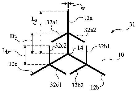
Figure 3 is a top view schematically showing an embod-
iment of an elementary conductive pattern 31 of a frequency-
selective surface.
As an example, the conductive material may be alumi-
num, gold, copper, silver, carbon, iron, platinum, graphite, or
a conductive alloy of several of these materials. Generally, the
higher the electric conductivity of the material, the better the
filtering performed by the surface.
Pattern 31, formed on a surface of a dielectric
support 10, comprises a basic tripole formed of three approxi-
mately identical segments 12a, 12b, and 12c of length Ls,
extending in a star from a center 14. Segments 12a to 12c form,
two-by-two, angles of approximately 1200, for example, ranging
between 110 and 130 .
Pattern 31 further comprises, for each segment 12a,
12b, 12c, two substantially identical branches, respectively
32a1 and 32a2, 32b1 and 32b2, and 32c1 and 32c2, extending from
an intermediate point of the segment, substantially symmetri-
cally with respect to the segment direction. In this example,
branches 32 have the shape of bars with a length Lb. On each
segment 12, the intermediate point is located approximately at a
same distance Db from center 14. The general directions of the
two branches 32 form an angle of approximately 120 , for exam-
ple, ranging between 110 and 130 , and defining an arrowhead
directed towards the outside of the pattern. Further, branches
32 associated with two different segments 12 are non secant.
Figure 4 is a top view schematically showing a portion
of an embodiment of a frequency-selective surface formed by the
repeating, according to a periodic layout on dielectric support
10, of elementary pattern 31 of Figure 3. Pattern 31 is repeated
by translation along each of the directions of segments 12a to
CA 02797559 2012-10-25
7
12c of the basic tripole, so that a same non-zero distance Dm
separates each outer end of a segment of a pattern 31 from
center 14 of a neighboring pattern 31. The translation operation
is repeated until the entire targeted surface is covered. It
should be noted that the dimensions of the elementary pattern
and distance Dm are selected to be such that the elementary
patterns are separate.
The frequency response of the surface thus formed
essentially depends on length Ls of segments 12, on length Lb of
branches 32, on distance Db between the intermediate starting
point of branches 32 of a segment 12 and center 14 of the
pattern, and on distance Dm between neighboring patterns.
The inventors have observed that such a surface has
three main resonance frequencies. The first resonance frequency
essentially depends on length Ls of segments 12 and on distance
Dm between neighboring patterns. The second resonance frequency
essentially depends on length Lb of branches 32 and on distance
Db between center 14 of the pattern and the intermediate point
of segment 12 from which the branches originate. The third reso-
nance frequency depends on all the above-mentioned parameters.
Such a surface has the property of filtering the elec-
tromagnetic waves belonging to three different frequency bands
centered on its three main resonance frequencies. In practice, a
simulation software is used to test different combinations of
parameters by performing progressive adjustments to obtain a set
of parameters adapted to the targeted frequency bands.
In the embodiment of Figure 4, the setting of the
first and second resonance frequencies is relatively easy, but
it is difficult to adjust the third resonance frequency without
modifying the first two frequencies.
Further, the three resonance frequencies of the
surface of Figure 4 remain slightly dependent on the angle of
incidence and on the polarization of electromagnetic waves.
Figure 5 is a top view schematically showing another
embodiment of an elementary conductive pattern 51 of a
CA 02797559 2012-10-25
8
frequency-selective surface. Pattern 51 shows all the elements
of pattern 31 of Figure 3. It further comprises two substan-
tially identical fins of length Las, respectively 52al and 52a2,
52b1 and 52b2, and 52cl and 52c2, extending from the outer end
of each segment 12, substantially symmetrically with respect to
the segment direction. Fins 52 of each segment 12 form together
an angle of approximately 1200, for example, ranging between 110
and 130 , and define an arrowhead directed towards the outside
of the pattern.
In an embodiment, pattern 51 further comprises two
substantially identical fins of length Lab, respectively 54al1
and 54a12, 54a21 and 54a22, 54bll and 54b12, 54b2l and 54b22,
54c1l and 54c12, and 54c21 and 54c22, extending from the outer
end of each branch 32 (on the side of the branch opposite to the
segment from which it originates), substantially symmetrically
with respect to the general branch direction. Fins 54 of each
branch 32 form together an angle of approximately 120 , for
example, ranging between 110 and 130 , and define an outward-
pointing arrowhead. The pattern dimensions are selected so that
fins associated with different segments or branches are not
secant and do not intersect the other segments and branches of
the pattern.
Figure 5 shows, in dotted lines, a portion of a
pattern 51' corresponding to a translation of pattern 51 along
the direction of segment 12a of pattern 51. In this example,
fins 52 of the segment of pattern 51' closest to center 14 of
pattern 51 are located in the space delimited by segments l2b
and 12c and by branches 32b2 and 32cl of pattern 51. A non-zero
distance Dm separates center 14 of pattern 51 from the end of
the closest segment 12. It should be understood that other
patterns (not shown) of a frequency-selective surface are formed
similarly, by translation along the directions of the other seg-
ments 12, according to a periodic layout of the type described
in relation with Figure 4.
CA 02797559 2012-10-25
9
The surface thus formed has three main distinct reso-
nance frequencies. These three resonance frequencies are inde-
pendent from the angle of incidence and from the polarization of
electromagnetic waves. Further, the introduction of additional
parameters Las and Lab relative to the length of fins 52 and 54
increases resonance frequency setting possibilities.
The strong interleaving of the elementary patterns is
considered to contribute to ensuring a behavior of the surface
independent from the angle of incidence and from the polariza-
tion of electromagnetic waves. Thus, it will be ascertained to
maintain parameter Dm relative to the distance between neighbor-
ing patterns relatively low.
Figure 6 is a top view schematically showing an alter-
native embodiment of the elementary conductive pattern of Figure
5. Pattern 61 of Figure 6 differs from the pattern of Figure 5
by the orientation of the fins associated with branches 32. In
pattern 61, two identical fins 64 (respectively 64all and 64a12,
64a21 and 64a22, 64bll and 64b12, 64b21 and 64b22, 64c11 and
64c12, and 64c21 and 64c22) associated with a branch 32 each
form an angle of approximately 60 , for example, ranging between
55 and 65 , with the general branch direction, and are substan-
tially aligned along a same direction, this direction intersect-
ing the direction of segment 12 from which branch 32 originates.
Like pattern 51 of Figure 5, pattern 61 provides
surfaces with three resonance frequencies. It especially enables
to obtain resonance frequencies different from those obtained
from pattern 51, and has the same setting possibilities and the
same insensitivity to the orientation and to the polarization of
electromagnetic waves as pattern 51.
Figure 7 is a top view schematically showing an alter-
native embodiment of the elementary conductive pattern of Figure
6. Pattern 71 of Figure 7 differs from the pattern of Figure 6
by the shape of the branches originating from segments 12.
Pattern 71 comprises two branches 72 (respectively 72al and
72a2, 72bl and 72b2, and 72cl and 72c2) extending from an inter-
CA 02797559 2012-10-25
mediate point of each segment 12 along the same general direc-
tion as branches 32 of the pattern of Figure 6. However, unlike
branches 32 of the pattern of Figure 6, branches 72 comprise a
crenel-shaped extension of height Hc, extending along a direc-
5 tion approximately orthogonal to the general branch direction,
towards the outside of the pattern.
Like pattern 61 of Figure 6, pattern 71 provides
surfaces with three resonance frequencies. The provision of a
crenel-shaped extension on branches 72 enables to vary the
10 length of the branches more, which increases resonance frequency
setting possibilities. Further, in the same way as for patterns
51 and 61 of Figures 5 and 6, the resonance frequencies of the
surfaces obtained from pattern 71 are insensitive to the orien-
tation and to the polarization of electromagnetic waves.
As an example, by repeating pattern 71 according to a
periodic layout of the type described in relation with Figure 4,
the inventors have obtained a surface capable of shielding
frequencies on the order of 0.9 and 1.8 GHz, by using the
following parameters:
Parameter Ls Db Dm Lb W Las Lab He
Value (mm) 25 9.1 0.75 7.5 0.5 4 5.75 5.9
The inventors have further obtained a surface capable
of shielding frequencies on the order of 2.4 and 5.4 GHz by
using the following parameters:
Parameter Ls Db Dm Lb W Las Lab Hc
Value (mm) 9.6 3.6 0.5 2.9 0.25 2 1.6 1.8
The two above examples do not consider the third reso-
nance frequency, which however exists.
Figure 8 is a top view schematically showing an alter-
native embodiment of the elementary conductive pattern of Figure
7. In pattern 81 of Figure 8, each branch originating from a
CA 02797559 2012-10-25
11
segment of the basic tripole comprises three crenel-shaped
extensions of height Hc, extending along directions approxi-
mately orthogonal to the general branch direction, towards the
outside of the pattern.
As an example, by repeating pattern 81 according to a
periodic layout of the type described in relation with Figure 4,
the inventors have obtained a surface capable of shielding
frequencies on the order of 0.9, 1.8 GHz, and 2.1 GHz by using
the following parameters:
Parameter Ls Db Dm Lb W Las Lab He
Value (mm) 28.8 9.8 0.5 8.8 0.5 6.3 0.05 5
Figure 9 is a top view schematically showing an alter-
native embodiment of the elementary conductive pattern of Figure
8. In pattern 91 of Figure 9, each branch originating from a
segment of the basic tripole comprises crenel-shaped extensions
of different heights, extending along directions approximately
orthogonal to the general branch direction, alternately towards
the outside and towards the inside of the pattern. Further, in
pattern 91, the fins associated with the branches are arranged
in an arrow, as in pattern 51 of Figure 5.
Figure 10 is a diagram illustrating the variation,
according to frequency, of the transmission factor (in decibels)
of a surface formed by the repeating of an elementary pattern 51
of Figure 5, for electromagnetic waves having different angles
of incidence. Curves 101, 102, and 103 show the frequency
responses of the surface for electromagnetic waves oriented
along directions respectively forming angles of 0, 30, and 60
with the direction orthogonal to the surface plane. The selec-
tion of the parameters is such that the surface has three
different resonance frequencies, respectively on the order of
0.9, 1.8, and 2.1 GHz. The diagram of Figure 10 shows that the
resonance frequencies of the surface, corresponding to negative
peaks in curves 101, 102, 103, are independent from the angle of
CA 02797559 2012-10-25
12
incidence of waves. It should further be noted that the reso-
nance frequencies are also independent from the wave polari-
zation.
According to a preferred embodiment, the frequency-
selective surfaces described hereabove are formed on paper- or
cardboard-type supports, for example, on wall paper, on paper or
cardboard lining plasterboards lined with cardboard, or on any
other support capable of lining the walls of a room of a build-
ing. The conductive patterns are for example formed by printing
with conductive inks.
According to an advantage of the above-described
frequency-selective surfaces, the coverage rate of the conduc-
tive patterns is relatively low, for example, smaller than 15%.
This enables to maintain a relatively low manufacturing cost for
such surfaces.
Specific embodiments of the present invention have
been described. Various alterations, modifications, and improve-
ments will readily occur to those skilled in the art.
In particular, the elementary conductive patterns
described in relation with Figures 7 to 9 may give rise to
several variations. However, for each of these patterns, it may
be chosen to arrange the fins associated with the branches of
the pattern either in an arrow, as described in relation with
Figure 5, or aligned along a same direction, as described in
relation with Figure 6. Further, it will be within the abilities
of those skilled in the art to implement the desired operation
by varying the number, the direction, and the orientation of the
crenel-shaped extensions formed of the pattern branches.
Further, in the elementary patterns described in rela-
tion with Figures 3 to 9, a second generation of symmetrical
branches originating from the main branches (32, 72) may be
provided to increase resonance frequency setting possibilities.