Note: Descriptions are shown in the official language in which they were submitted.
CA 02797840 2012-10-29
WO 2011/136653 PCT/NL2011/050294
Light-emitting device and method for manufacturing the same.
BACKGROUND OF THE INVENTION
Field of the invention
The present invention relates to a light-emitting device.
The present invention further relates to a method for manufacturing a light-
emitting
device.
Related Art
Organic light emitting devices ("OLEDs"), including both polymer and small-
molecule OLEDs, are potential candidates for a great variety of virtual- and
direct-
view type displays, such as lap-top computers, televisions, digital watches,
telephones, pagers, cellular telephones, calculators and the like. Unlike
inorganic
semiconductor light emitting devices, organic light emitting devices are
generally
simple and are relatively easy and inexpensive to fabricate. Also, OLEDs
readily
lend themselves to applications requiring a wide variety of colors and to
applications
that concern large-area devices.
OLEDs generate light when an electron and a hole combine in a light-
emitting layer in the OLED to generate a photon. The percentage of combined
electrons and holes that result in generation of a photon in the light-
emitting layer
is referred to as the "internal electroluminescence quantum efficiency." The
percentage of generated photons that are transmitted or "coupled" out of the
device
is referred to as the "external electroluminescence quantum efficiency" or the
"out-
coupling" efficiency of the device. Models predict that only about 20% or less
of the
generated photons are transmitted out of the device. It is believed that this
is at
least in part due to the fact that the generated photons are trapped within
the
OLED device by internal reflection at interfaces within the OLED, resulting in
waveguiding of the photons within the OLED and absorption of the trapped
photons
by the OLED. Absorption can occur within any part of the OLED device, such as
within an ITO anode layer or within the substrate. Internal reflection occurs
where
the refractive index of that particular part is greater than the refractive
indices of
CA 02797840 2012-10-29
WO 2011/136653 PCT/NL2011/050294
2
the adjacent parts. These phenomena result in decreased external
electroluminescence quantum efficiency and a reduction in the luminescence or
brightness in directions extending outwardly from the surface of the device.
US 2003127973 describes an OLED that is provided with a composite barrier
layer disposed over the active region and/or on a surface of the substrate.
The
composite barrier layer comprises an alternating series of one or more
polymeric
planarizing sublayers and one or more high-density sublayers. At least one of
the
polymeric planarizing sublayers has microparticles incorporated therein. This
includes preferably the polymeric planarizing sublayer closest to the active
region.
The microparticles are effective to increase the out-coupling efficiency of
the OLED.
The microparticles are preferably comprised of a transparent material,
preferably an
inorganic material such as a metal, metal oxide, e.g., Ti02, or other ceramic
material having a relatively high index of refraction, preferably, the
microparticles
will have an index of refraction of greater than about 1.7. The microparticles
are
preferably substantially smaller than the largest dimension of any active
region or
pixel in a display comprising an OLED device of the invention. The
microparticles
preferably will have a size greater than the wavelength a,, of light generated
by the
OLED. Thus, the microparticles will preferably have a particle size greater
than
about 0.4 m-0.7 m. The microparticles will preferably have a size in the
range of
from about 0.4 pm to about 10 m or greater. The presence of the
microparticles
reduces the planarizing effect of the planarizing layer.
It is noted that US2009/302744 Al discloses an OLED device and a
manufacturing method thereof. Organic light emission diode elements are
disposed
on a substrate. On the substrate with the organic light emission diode
elements, a
sealant layer having a micro-lens portion is disposed, thereby shielding the
organic
light emission diode elements from external moisture and/or oxygen. The
sealant
layer is formed of a pre-composition that includes a liquid pre-polymer. In an
embodiment the sealant layer is sandwiched between two auxiliary sealant
layers.
An auxiliary sealant layer can be one of a silicon oxide film and a silicon
nitride, or a
stacked layer thereof.
It is further noted that US-9005/194896 Al discloses light-emitting device
with a light extraction layer formed by a transparent medium dispersed with a
fine
CA 02797840 2012-10-29
WO 2011/136653 PCT/NL2011/050294
3
transparent substance whose refractive index differs from that of the
transparent
medium.
SUMMARY OF THE INVENTION
It is an object of the invention to at least partially overcome the
disadvantages of the prior art.
According to a first aspect of the invention there is provided a light-
emitting
device comprising
an organic light-emitting diode structure,
an encapsulation comprising a light-transmitting window with at least a first
inorganic layer, an organic layer and a second inorganic layer, the organic
layer
comprising domains of a dispersed first organic component embedded by a second
component, the first and the second component having a mutually different
refractive index, the organic layer being sandwiched between the first and the
second inorganic layer.
According to a second aspect of the invention there is provided a method for
manufacturing a light-emitting device, comprising the steps of
- providing a light-emitting structure,
providing an encapsulation comprising the step of providing a light-
transmitting window by
providing at least a first inorganic layer,
providing an organic layer composed of at least a first and a second
organic component having a mutually different refractive index, wherein the at
least
first component is dispersed as domains that are embedded by the at least
second
component in the composite organic layer,
curing the organic layer and
providing a second inorganic layer.
The device and method as claimed are non-obvious in view of the following
arguments.
As the OLED device known from US2009/0302744 already has a layer with
micro-lens portions that is intended to improve light-output efficiency, the
skilled
CA 02797840 2012-10-29
WO 2011/136653 PCT/NL2011/050294
4
person in this field has no incentive to apply a light extraction layer as
disclosed in
US2005/194896.
Moreover, according to 218, 219 of the latter patent publication, the
structure of the light extraction layer has the effect that light is
scattered.
US2009/0302744 on the contrary aims to avoid a blurring phenomenon. See for
example 50, 51, 55. Accordingly these patent publications have a mutually
conflicting teaching therewith discouraging the skilled person to apply the
light
extraction layer of US2005/194896 to the device of US200910302744.
The organic layer typically has a thickness between 5 and 200 m. The
inorganic layers are in practice substantially thinner than the organic
layers. An
organic layer substantially thinner than 5 m, e.g. 1 m does not provide for a
sufficient planarization. An organic layer substantially thicker than 200 m,
e.g.
thicker than 500 m may result in an unnecessary absorption of radiation. The
inorganic layers typically have a thickness in the range of 100 to 300 nm. An
inorganic layer substantially thinner than 100 nm, e.g. smaller than 10 nm
would
require deposition of the inorganic layer with a high density, which
necessitates
dedicated deposition techniques. Deposition of an inorganic layer
substantially
thicker than 300 nm, e.g. thicker than 1000 nm would require an unnecessary
long
deposition time as it provides no significant improvement of the functionality
of the
barrier structure. Moreover, a thick inorganic layer is unfavorable for the
translucence of the barrier structure.
An organic layer having dispersed domains of a first component that are
embedded by a second component may be obtained by preparing a dispersion of at
least first liquid organic substance into at least a second liquid organic
substance,
which liquid organic substances are mutually immiscible and applying the
dispersion at the at least a first inorganic layer. Immiscible organic
substances are
considered to be organic substances that substantially do not dissolve into
each other.
In this embodiment of the method the first organic substance is dispersed in
the
second organic substance, for example by stirring, before it is applied at the
inorganic layer. This has the advantage that the average size of the domains
formed
by the first component and therewith the optical properties of the organic
layer can
be controlled when forming the dispersion. The two mutually immiscible
substances
CA 02797840 2012-10-29
WO 2011/136653 PCT/NL2011/050294
in the organic layer may include a polar organic substance and a non-polar
substance. In addition two or more organic substances may be present in the
composition used for providing the organic layer.
In another embodiment of the method the step of curing the organic layer
5 causes a phase separation resulting in formation of the domains of the first
component embedded by the second component. In that case the organic
substances
used for preparing the organic layer may be mutually miscible. This has the
advantage that they can be prepared as a stable mixture that is immediately
available for use in the manufacturing process. The mixture may even be stored
in
the printing unit used for applying the organic layer, therewith avoiding the
necessity to clean the printing unit when not in use. An example of such
mutually
miscible substances result in formation of domains of mutually different
phases
upon curing is described by E. Arevalo et al. "Epoxy/poly(benzyl methacrylate)
blends: miscibility, phase separation on curing and morphology", in
Proceedings of
the 8th Polymers for Advanced Technologies International Symposium, Budapest,
Hungary, 13-16 September 2005.
The organic layer comprising domains of a dispersed first organic component
embedded by a second component, the first and the second component having a
mutually different refractive index causes radiation emanating from the
organic
light-emitting diode structure to be refracted at the interfaces of these
components.
Radiation that otherwise would be reflected by total internal reflection is
now
distributed over a range of angles, so that it can escape at least partly
through the
light-transmitting window. Use of this organic layer has resulted in
enhancements
in the OLED-output as large as 40%. The enhancement by application of an
organic
layer provided with scattering particles is limited to about 25%, see for
example R.
Bathelt et al. Organic Electronics 8 (2007), p.p. 293-299.
It is furthermore an advantage that the dispersion can be applied in liquid
form due to the fact that the substances used are organic. For example the
substances can be in a solved or in a molten state. Alternatively liquid
organic
substances may be used that are subsequently cured by polymerizing for
example. If
desired one of the organic substances may remain in liquid form as islands in
the
solid sea formed by the other substance. As the dispersion can be applied in a
liquid
form it can be easily planarized, contrary to mixtures comprising solid
particles.
CA 02797840 2012-10-29
WO 2011/136653 PCT/NL2011/050294
6
Additionally using the dispersion is advantageous for manufacturing processes,
e.g.
printing as it tends less to stick to the manufacturing machinery.
Various combinations of mutually immiscible organic materials are known as
such, in particular for obtaining an improved mechanical properties, but their
use as
an organic layer between a pair of inorganic layers in a barrier structure for
improvement of lightoutcoupling of an organic light-emitting diode has been
unknown until now. For example EP0488374 discloses a composition comprising an
epoxy resin and a curing agent that is blended with a thermoplastic resin
impregnated with an organic silicon compound to provide an epoxy resin
composition
which cures into products having improved adhesion and thermal impact and is
suitable for encapsulating semiconductor devices. EP0488374 observes that "the
attainment of an epoxy resin composition having a high glass transition
temperature,
a low coefficient of expansion and high crack resistance is largely due to the
fact that
the epoxy-silicone resin copolymer is immiscible with the (curable) epoxy
resin, but
assumes a sea-island structure in the epoxy resin composition."
Suitable materials for the first and the second inorganic layers between
which the organic layer composed of a dispersion of at least two mutually
immiscible
transparent organic substances is arranged include, but are not limited to,
metal
oxides, metal nitrides, metal carbides, metal oxynitrides, metal oxyborides,
and
combinations thereof. The metal oxides are preferably selected from silicon
oxide,
aluminum oxide, titanium oxide, indium oxide, tin oxide, indium tin oxide,
tantalum
oxide, zirconium oxide, niobium oxide, and combinations thereof. The metal
nitrides
are preferably selected from aluminum nitride, silicon nitride, boron nitride,
and
combinations thereof. The metal oxynitrides are preferably selected from
aluminum
oxynitride, silicon oxynitride, boron oxynitride, and combinations thereof. In
unilateral light-emitting devices opaque barrier layers can be used for the
non-
emitting side of the device. Opaque barrier inorganic materials materials
include,
but are not limited to, metals, ceramics, polymers, and cermets. Examples of
opaque
cermets include, but are not limited to, zirconium nitride, titanium nitride,
hafnium
nitride, tantalum nitride, niobium nitride, tungsten disilicide, titanium
diboride, and
zirconium diboride.
It is noted that US7,109,651 discloses an organic electroluminescence cell
including at least one organic layer and a pair of electrodes. The organic
layer
CA 02797840 2012-10-29
WO 2011/136653 PCT/NL2011/050294
7
includes a light-emitting layer that is sandwiched between the pair of
electrodes.
The pair of electrodes include a reflective electrode and a transparent
electrode. The
organic electroluminescence cell is formed to satisfy the expression; Bo<Be in
which
Bo is a frontal luminance value of luminescence radiated from a light
extraction
surface to an observer, and Be is a luminance value of the luminescence at an
angle
of from 50 DEG to 70 DEG. A reflection/refraction angle disturbance region is
provided so that the angle of reflection/refraction of the luminescence is
disturbed
while the luminescence is output from the light-emitting layer to the observer
side
through the transparent electrode. The organic electroluminescence cell is
provided
with a region for disturbing the angle of reflection/refraction of light
between the
light-emitting layer and an output medium on the observer side. In an
embodiment
the region comprises a dispersion of microdomains. From the point of view of
the
dispersion/distribution of micro domains, a combination such as brings phase
separation is preferred. The dispersion/distribution can be controlled on the
basis of
mutual solubility of materials combined. The phase separation can be performed
by
a suitable method such as a method of dissolving mutually insoluble materials
in a
solvent or a method of mixing mutually insoluble materials while thermally
melting
the mutually insoluble materials. US7109651 does not recognize that the region
can
be applied in a barrier structure as a planarizing layer between a first and a
second
inorganic layer.
BRIEF DESCRIPTION OF THE DRAWINGS
These and other aspects are described in more detail with reference to the
drawing.
Therein:
FIG. 1 shows a cross-section through a first embodiment of a light-emitting
device according to the first aspect of the present invention,
FIG. 2 shows a SEM picture corresponding to a cross-section according to 11-
11 in FIG. 1,
FIG. 2A shows the cross-section according II-II in FIG. 1 more schematically,
FIG. 3 shows an AFM picture corresponding to a cross-section II-II in FIG. 1,
FIG. 3A is an EEDX picture according to view III in FIG. 1,
CA 02797840 2012-10-29
WO 2011/136653 PCT/NL2011/050294
8
FIG. 4A, 4B and 4C describe a first, a second and a third mode of
measurement for measuring outcoupling efficiency of the light-emitting device,
FIGs 5A to 5L show an embodiment of a method according to a second aspect
of the present invention.
DETAILED DESCRIPTION OF EMBODIMENTS
In the following detailed description numerous specific details are set forth
in
order to provide a thorough understanding of the present invention. However,
it will
be understood by one skilled in the art that the present invention may be
practiced
without these specific details. In other instances, well known methods,
procedures,
and components have not been described in detail so as not to obscure aspects
of the
present invention.
The invention is described more fully hereinafter with reference to the
accompanying drawings, in which embodiments of the invention are shown. This
invention may, however, be embodied in many different forms and should not be
construed as limited to the embodiments set forth herein. Rather, these
embodiments are provided so that this disclosure will be thorough and
complete, and
will fully convey the scope of the invention to those skilled in the art. In
the
drawings, the size and relative sizes of layers and regions may be exaggerated
for
clarity. Embodiments of the invention are described herein with reference to
cross-
section illustrations that are schematic illustrations of idealized
embodiments (and
intermediate structures) of the invention. As such, variations from the shapes
of the
illustrations as a result, for example, of manufacturing techniques and/or
tolerances,
are to be expected. Thus, embodiments of the invention should not be construed
as
limited to the particular shapes of regions illustrated herein but are to
include
deviations in shapes that result, for example, from manufacturing. Thus, the
regions
illustrated in the figures are schematic in nature and their shapes are not
intended
to illustrate the actual shape of a region of a device and are not intended to
limit the
scope of the invention.
As used herein, a "layer" of a given material includes a region of that
material whose thickness is small compared to both its length and width.
Examples
of layers include sheets, foils, films, laminations, coatings, and so forth.
As used
CA 02797840 2012-10-29
WO 2011/136653 PCT/NL2011/050294
9
herein a layer need not be planar, but can be bent, folded or otherwise
contoured, for
example, to at least partially envelop another component. As used herein a
layer can
also include multiple sub-layers. A layer can also consist of a collection of
discrete
portions, for example, a layer of discrete active regions comprising
individual pixels.
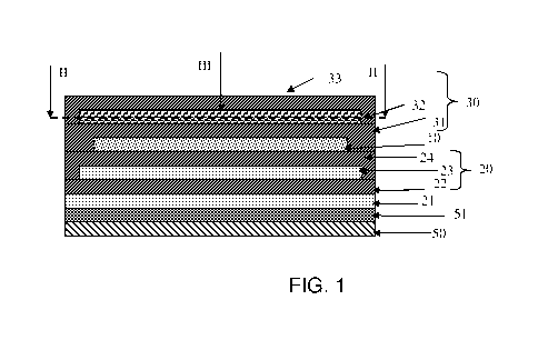
FIG. 1 shows a light-emitting device comprising an organic light-emitting
diode structure 10. The light emitting diode structure 10 is encapsulated by a
first
and a second barrier structure 20, 30. The light emitting diode structure for
example
subsequently comprises the following layers an anode formed by an indium tin
oxide
(ITO) layer having a thickness of about 120 nm, a PEDOT layer having a
thickness
of about 100 nm, a light emitting polymer layer (LEP) having a thickness of 80
nm
and a cathode layer having a barium sub-layer (5nm) and an aluminium sub-layer
(100nm). The first barrier structure 20 comprises a first inorganic layer 21,
an
organic layer 22 and a second inorganic layer 23. The second barrier structure
30
comprises a first inorganic layer 31, an organic layer 32 and a second
inorganic layer
33. The light-emitting device is mounted via a first and a second intermediate
layer
21, 51 at a substrate 50. If desired the substrate may be removed.
The second barrier structure 30 with first inorganic layer 31, organic layer
32 and
second inorganic layer 33 of the encapsulation 20, 30 forms a light-
transmitting
window. The organic layer 32 of the second barrier structure is composed of a
dispersion of at least two mutually immiscible organic substances. In this
example
the inorganic layers 31, 33 have a thickness of 150 nm and are formed of SiN.
The
organic layer 32 has a thickness of 100 m.
FIG. 2 shows a SEM picture corresponding to a cross-section through the
organic layer 32 according to II-II in FIG. 1.
In the embodiment shown the dispersion comprises a mixture of two epoxy
silicon resins (90.5 w%) and a cycloaliphatic epoxy resin (7.5 w%). In
addition the
dispersion comprises 2 w% of photo-initiator. In this composition the two
silicon
epoxy resins are miscible (they give a clear solution and film), the epoxy
resin 1 is
not miscible with the cycloaliphatic epoxy (gives a white solution and film)
and the
epoxy silicon 2 is miscible with the cycloaliphatic epoxy resin (gives a clear
solution
and film). Suitable materials to produce the organic layer 32 can be found for
example in the European patent application 10161452.7.
CA 02797840 2012-10-29
WO 2011/136653 PCT/NL2011/050294
The transparent organic substances in the organic layer forms micrometer-sized
phase-separating domains that have a mutually different refractive index, so
that
light is refracted at the interfaces between these phase separating domains.
As also shown schematically in FIG. 2A, the first and second organic
substances
5 form a sea-island structure having an island phase 32a (dark-gray in the
picture)
and a sea phase 32b (light-grey in the picture).
FIG. 3 shows an AFM-picture of the organic layer 32. In this picture only the
island phase 32a is shown. From this picture it becomes clear that the island
phase
10 32a is shaped as lens like elements.
A surface analysis was carried out to determine the composition of the phases
in the organic layer. FIG. 3A illustrates the distribution of Si at the
surface of the
layer. Therein relatively bright zones having a relatively high Si content and
relatively dark zones have a relatively low Si content.
A more detailed measurement indicated in mass percent the following
distribution of the elements C, 0 and Si for the island phase (ID1) and the
sea-phase
(ID2), as shown in the following table.
Table 1: distribution of the elements C, 0 and Si in the phases of the organic
layer.
Spectrum C 0 Si
ID 1 54.33 29.51 16.15
ID2 37.38 35.25 27.36
From the table it can be concluded that the sea-phase is relatively Si-rich in
comparison to the island phase.
The improvement of a light-output of the light-emitting device provided with
an organic layer comprising a dispersion of mutually immiscible transparent
organic
substances was compared with that of a same light-emitting device without such
a
layer. The light-output was also compared with that of a light-emitting device
having a commercially available light-outcoupling foil provided with micro-
lenses.
A hybrid white OLED at colour point A (Warm White) with a very good
uniformity was used for the tests. The optical output of the white OLED (0)
was
measured on a special mount in an integrating sphere ISB 500 from Instrument
CA 02797840 2012-10-29
WO 2011/136653 PCT/NL2011/050294
11
Systems of 50 cm diameter and was analyzed with a CAS 140 B spectrometer. In
the
planar case only the radiation from the front face of the OLED was taken into
account, emission from the sides was blocked. To obtain the light emitted into
the
substrate a half-sphere macro extractor (diameter 100 mm) was attached to the
substrate with an index matching fluid. The measurements were performed at
identical currents for all 3 measurement modes of FIG. 4, at a brightness of
about
1000 cd/m2 in the planar (blank) case. FIG. 4A shows a planar mode with sides
taped. FIG. 4B shows a mode with a surface scattering structure (S), here
shown as
a corrugated layer, either on glass or directly on the OLED and FIG. 4C shows
the
measurement with a half-sphere macro-extractor (H). The emitting area of the
OLED is 10,65 cm2. The improvement is given as the ratio of the respective
luminance to the blank reference without emission to the sides. From this ILO
(in %)
is derived as the relative difference to the reference. Outcoupling efficiency
OE is the
percentage coupled into air of light in glass substrate (measured with half
sphere
macro extractor). The results are shown in Table 2.
Table 2: Measurement results
Out-coupling structures Improvement Outcoupling
(ILO) efficiency OE
Plane, sides closed* Ref.: 0 % 52,3 %
Half sphere macro extractor + 91,2 % 100 %
JB2-10B, with sugar water +33,0% 69,6 %
JB2-10B, with Cargille n=1,53 +39,2% 72,8 %
JB2-10B with 3M glue on glass +30,8%, 68,4 %
0,7mm on Cargille fluid
JB2-10B, with 3M glue on glass + +37,3% 71,8 %
Cargille fl., sides open
BIC micro-lens array*, Cargille fl. +40,4%, 73,5 %
In this measurement a foil denoted as JB2-10B is used having the same
composition
as the organic layer in the second barrier structure of the device according
to the
invention was optically attached either with sugar water (n=1,4, but
birefringent) or
CA 02797840 2012-10-29
WO 2011/136653 PCT/NL2011/050294
12
with an index matching fluid Cargille Series A; n=1,53; Also a double-sided
adhesive foil from 3M was used, but on top of a float glass plate of 0,7 mm
thickness.
As can be seen in the table the output efficiency of the OLED provided with
the foil
J132-10B is significantly improved to about 70% as compared to the output
efficiency
(52,3%) of the reference situation. The output efficiency so obtained is
comparable to
that for the commercially available outcouple foil that uses micro-lenses.
FIGs 5A to 5L describe a possible method of manufacturing a device
according to the invention.
In step S1, illustrated in FIG. 5A a substrate 50 is provided. According to
the
invention the substrate is made of an inorganic material. The inorganic
material
may comprise e.g. a ceramic material, a glass or a metal.
In step 5B a release layer 51 is applied on the substrate 50. The methods
described
above for applying an organic layer are suitable for this purpose.
The release layer 51 may comprise a silica organic based polymer such as
polydimethylsiloxane (PDMS), but may alternatively comprise another component
that provides for a sufficient adhesion of the workpiece to the substrate 50
during
manufacturing, but that allows an easy release of the workpiece once finished.
Surprisingly, also materials used in the active layers of OLED devices, like
PEDOT
and LEP turned out to be suitable for this purpose. At release of the finished
product
from the substrate 50, the release layer 51 may stay with the product, or may
stay
with the substrate 50. If the release layer 51 stays with the substrate 50 it
may be
reused or removed.
In steps S3 to S5 shown in FIGs 5D to 5F respectively, a first barrier
structure 20, comprising layers 21, 22, 23, is applied at the release layer
51. In the
embodiment shown these steps comprise:
Step S4, shown in FIG. 5D, wherein a first inorganic layer 22 is applied,
Step S5, shown in FIG. 5E, wherein a first organic layer 23 is applied at the
first
inorganic layer 22, and
Step S6, shown in FIG. 5F wherein a second inorganic layer 24 is applied at
the first
organic layer 23.
In this case step S4 is preceded by an additional step S3, shown in FIG. 5C,
wherein an additional organic layer 21 is applied at the release layer 51, so
that the
first inorganic layer 22 is applied at the additional organic layer 21.
CA 02797840 2012-10-29
WO 2011/136653 PCT/NL2011/050294
13
In step S7, shown in FIG. 5G, an organic light emitting diode 10 is
constructed. The construction thereof is well known as such to the skilled
person,
and is therefore not described in detail here.
In steps S8 to S11 a second barrier structure 30 is applied on top of the
organic thin film electronic device.
These steps comprise:
Step S8, shown in FIG. 5H, wherein a third inorganic layer 31 is applied,
Step S9, shown in FIG. 51, wherein a second organic layer 32 is applied at the
third
inorganic layer 31. The second organic layer 32 is applied as a dispersion of
a first
and a second mutually immiscible transparent organic substance. In this
dispersion
the first transparent organic substance comprises a mixture of two epoxy
silicon
resins (90.5 w%) and the second transparent organic substance is an
cycloaliphatic
expoxy resin (7.5 w%). In addition the dispersion comprises 2 w% of photo-
initiator.
The components were mixed simultaneously by stirring with a magnetic stirrer
(Heidolph MR Hei-End) at 500 rpm for about 10 min. Subsequently the
formulation
was applied on a bar-coater (RK Control coater) using a plastic pipet, and
then
applied as a film using the 100 micrometers wire bar. After stirring the
island phase
32a having a relatively low silicon content is finely distributed within the
sea phase
32b having a relatively high silicon content. The finely distributed island
phase 32a
forms microlenses having a diameter in the range of 1 to 10 m. By stirring
for a
longer time a finer distribution is obtained. Stirring for a shorter time
results in a
courser distribution.
As shown in FIG. 5J, in a next step S10 the organic layer 32 so applied is
cured by radiation with an UVA-source providing a radiation dose of 3J/cm2.
In Step 511, shown in FIG. 5K, a fourth inorganic layer 33 is applied at the
first
organic layer 32.
In a subsequent step S12, shown in FIG. 2L, the product formed in the previous
steps is released from the substrate 50. Therewith an encapsulated electronic
device
as shown in FIG. 1 is obtained. As shown in FIG. 1A more devices may be
constructed on a single substrate 50.
In the above-described method of manufacturing the inorganic layers may be
applied by all kinds of physical vapour deposition methods such as thermal
CA 02797840 2012-10-29
WO 2011/136653 PCT/NL2011/050294
14
evaporation, e-beam evaporation, sputtering, magnetron sputtering, reactive
sputtering, reactive evaporation, etc. and all kinds of chemical vapour
deposition
methods such as thermal chemical vapour deposition (CVD), photo assisted
chemical
vapour deposition (PACVD), plasma enhanced chemical vapour deposition (PECVD),
etc.
The organic layers may be applied by all kinds of coatings techniques, such
spin coating, slot-die coating, kiss-coating, hot-melt coating, spray coating,
etc. and
all kinds of printing techniques, such as inkjet printing, gravure printing,
flexographic printing, screen printing, rotary screen printing, etc. Also the
second
organic layer 32 comprising a dispersion of mutually immiscible transparent
organic
substances may be applied by one of these methods. It is therewith an
advantage
that the dispersion comprises no solid particles, so that sedimentation of
components
in the organic substance is counteracted.
For clarity it is not illustrated in the figures how the electronic device 10
is
electrically connected to external conductors. Preferably the electrical
conductors to
the electronic device are provided as an aluminum conductor with a molybdenum
coating between subsequent inorganic layers 24, 21 for example. The molybdenum
coating therein serves as an adhesion layer. This step of applying the
electrical
conductors can be applied between step S7 and S8 according to the method
described
above. In an alternative embodiment an electrical connection to outside
conductors
is provided later, e.g. after step 2K. This is possible by punching respective
holes
through at least one of the barrier layers towards electrical connectors of
the
electronic device and filling these holes with a conductive material.
Although in the embodiment shown the light-emitting device is released from
the substrate 50 it is in another embodiment possible to maintain the light-
emitting
device to the substrate. In that case the release layer 51 may be omitted.
Also the
additional organic layer 21 may be omitted. In an embodiment the first barrier
structure 20 alternatively or additionally is provided with an organic layer
23
comprising a dispersion of mutually immiscible transparent organic substances.
In
again another embodiment the barrier structure 20 is replaced by a metal foil
or a
glass plate for example.
CA 02797840 2012-10-29
WO 2011/136653 PCT/NL2011/050294
It is not necessary that the light-emitting structure is provided first. In an
embodiment first the light-transmitting window is provided and the light-
emitting
structure is applied at the light-transmitting window.
It will be understood that the terms "comprises" and/or "comprising," when
5 used in this specification, specify the presence of stated features,
integers, steps,
operations, elements, and/or components, but do not preclude the presence or
addition of one or more other features, integers, steps, operations, elements,
components, and/or groups thereof. In the claims the word "comprising" does
not
exclude other elements or steps, and the indefinite article "a" or "an" does
not
10 exclude a plurality. A single component or other unit may fulfill the
functions of
several items recited in the claims. The mere fact that certain measures are
recited
in mutually different claims does not indicate that a combination of these
measures
cannot be used to advantage. Any reference signs in the claims should not be
construed as limiting the scope.
15 Further, unless expressly stated to the contrary, "or" refers to an
inclusive or
and not to an exclusive or. For example, a condition A or B is satisfied by
any one of
the following: A is true (or present) and B is false (or not present), A is
false (or not
present) and B is true (or present), and both A and B are true (or present).