Note: Descriptions are shown in the official language in which they were submitted.
CA 02799785 2015-02-19
IMPROVED ORTHOGONAL FREQUENCY-DIVISION MULTIPLEXING (OFDM)
COMMUNICATION SLOT STRUCTURES AND METHODS
FIELD OF THE DISCLOSURE
[0002] This disclosure relates generally to mobile communications and,
more
particularly, to improved communication slot structures and methods.
BACKGROUND
[0003] Currently known or proposed techniques for allowing orthogonal
frequency-
division multiplexing (OFDM) using the numerology of the current Enhanced
General Packet
Radio Service (EGPRS) utilize a single OFDM symbol within a time slot.
Additionally,
currently known or proposed techniques require spectral shaping at the edges
of the transmission
band and include a training symbol distribution that is not optimal for
channel estimation at the
edges of the transmission band.
BRIEF DESCRIPTION OF THE DRAWINGS
[0004] FIG. 1 is block diagram of an example mobile communication
system
including an example mobile station and an example network element
implementing methods
and apparatus to implement and utilize the improved communication slot
structures and methods
described herein.
[0005] FIG. 2 illustrates an example transmit lineup that may be used
by the mobile
station and/or the network element of FIG. 1.
[0006] FIG. 3 illustrates an example receive lineup that may be used by
the mobile
station and/or the network element of FIG. 1.
[0007] FIG. 4 illustrates an example signal generator that may be used
by the transmit
lineup of FIG. 2.
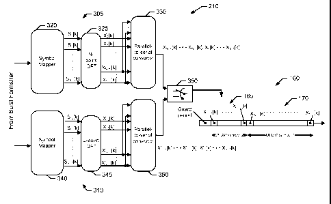
- 1 -
CA 02799785 2012-11-16
WO 2011/146396 PCT/US2011/036655
[0008] FIG. 5 and 6 illustrate example frequency and time domain
signals produced
by the signal generator of FIG. 4 to send information in two sub-slots.
[0009] FIGS. 7 and 8 illustrate example frequency and time domain
signals produced
by the signal generator of FIG. 4 to send information in two sub-slots using a
radix 2 allocation
of symbols in two sub-slots.
[0010] FIG. 9 illustrates an example frequency domain signal and an
example
allocation of modulation schemes to the sub-bands.
[0011] FIG. 10 illustrates an example converter/symbol mapper that may
use different
modulation schemes based on sub-band position within the frequency space
allocated to the
frame.
[0012] FIG. 11 illustrates example frequency domain signals produced by
the signal
generator of FIG. 4, showing an allocation of training and data symbols in two
sub-bands.
[0013] FIG. 12 is a flow diagram representing an example
encoding/modulation
process.
[0014] FIG. 13 is a flow diagram representing an example process of
burst formatting
code bits.
[0015] FIG. 14 is a flow diagram representing an example process of
mapping
frequency domain signals representing symbols.
[0016] FIG. 15 is a flow diagram representing an example
decoding/demodulation
process.
[0017] FIG. 16 is block diagram of an example processing system that
may execute
example machine readable instructions used to implement some or all of the
above processes.
DETAILED DESCRIPTION
[0018] Methods and apparatus to implement and utilize the improved
communication
slot structures described herein. Although the following discloses example
methods and
- 2 -
CA 02799785 2012-11-16
WO 2011/146396 PCT/US2011/036655
apparatus including, among other components, software executed on hardware, it
should be
noted that such methods and apparatus are merely illustrative and should not
be considered as
limiting. For example, it is contemplated that any or all of these hardware
and software
components could be implemented exclusively in hardware, exclusively in
software, exclusively
in firmware, or in any combination of hardware, software, and/or firmware.
Accordingly, while
the following describes example methods and apparatus, persons having ordinary
skill in the art
will readily appreciate that the examples provided are not the only way to
implement such
methods and apparatus.
[0019] The example methods and apparatus to implement and utilize an
improved
communication slot structure include subdividing a time division multiple
access (TDMA)
communication time slot into two or more sub-slots each of which is occupied
by a single
OFDM symbol. In a conventional arrangement, to remain unchanged compared to
the current art
enabling OFDM based communication in EGPRS slot structure (GP100364, Ericsson,
"Precoded
EGPRS2 Downlink," GERAN#45, Berlin, which is incorporated herein by
reference), all data to
be communicated during a time slot is carried during that time slot using a
defined set of sub-
carriers on a single OFDM symbol. As described herein, data and/or training
sequence symbols
for transmission may be communicated in the sub-slots, each occupied by an
OFDM symbol
which may be of unequal size. Because each sub-slot is of smaller duration
than the original
time slot but is sampled at the same rate, the spacing between each sub-
carrier in each OFDM
symbol is wider. For example, the current art consists of occupying a
conventional slot, such as
a Global System for Mobile Communications (GSM) time slot with a single OFDM
symbol
consisting of a cyclic prefix of 6 samples and a body of 142 samples in a
15/26 millisecond (ms)
burst resulting in 142 sub-carriers transporting 116 data symbols and 26
training sequence
symbols and where each sub-carrier is spaced apart by1.9 kilohertz (kHz). This
sub-carrier
spacing is quite small and can result in degrading the signal to noise ratio
experienced at each
sub-carrier at high speeds.
[0020] In the arrangements described herein, the same number of data
and/or training
sequence symbols may be carried in two sub-slots the total time duration of
which is 15/26 ms,
-3 -
CA 02799785 2012-11-16
WO 2011/146396 PCT/US2011/036655
wherein each of the sub-slots includes carriers having wider bandwidth spacing
than in a
conventional frame. For example, if the symbols from a conventional slot are
divided evenly
into two sub-slots each containing an OFDM symbol with a cyclic prefix length
of 6 samples and
OFDM symbol body of 68 samples, the bandwidth of the sub-carriers in each sub-
slot is twice as
wide as those of the conventional slot (e.g., 3.8 kHz vs. 1.9 kHz). However,
since 6 time domain
samples are used for the cyclic prefix in the second OFDM symbol, the total
number of sub-
carriers carried by the two OFDM symbols has now been reduced from 142 to 136
(or 68x2). In
this example, in order to transport the same 116 data symbols, the number of
training sequence
symbols is reduced from 26 to 20. In an alternative example, the number of
data symbols is
reduced to 110 data symbols and all 26 training sequence symbols are
transported.
[0021] In an alternate example the cyclic prefix of the second OFDM
symbol could be
obtained, or borrowed, from the guard period between bursts. Also, the cyclic
prefix need not be
an integer number of samples.
[0022] One division of symbols between sub-slots is to divide the
symbols such that
the number of time domain symbols in the OFDM body in each sub-slot is a power
of two (i.e.,
radix 2). The radix 2 division allows efficient time domain-to-frequency
domain transformations
(e.g., discrete Fourier transformation, fast Fourier transformation, etc.) at
the receiver. Thus, a
radix 2 number of symbols simplifies demodulation.
[0023] To comply with spectral emissions requirements of an EGPRS
burst,
amplitudes of sub-carriers at the edges of the frequency band carrying an
EGPRS burst are
attenuated when compared to the sub-carriers in the middle of the band. Uneven
attenuation
throughout the band carrying the EGPRS burst results in unequal error
protection for information
carried in the burst. Thus, there will be a lower signal to noise ratio or
higher bit error rate
(BER) at the frequency edges of the burst as compared to the center of the
burst if the same
modulation is used throughout. As described herein, different modulation
schemes may be used
between the center of the band and the edges of the band. For example, a
modulation scheme
such as binary phase shift keying (BPSK) or some other relatively low bits-per-
symbol
modulation scheme may be used at the edges of the band and a relatively high
bits-per-symbol
- 4 -
CA 02799785 2012-11-16
WO 2011/146396 PCT/US2011/036655
modulation scheme, such as 16-quadrature amplitude modulation (16-QAM) may be
used in the
relative middle of the band. In this manner, because the reduced density
modulation schemes
offer greater per bit protection for identical signal to noise ratios, the
uneven per bit error
protection due to uneven signal to noise ratio experienced by sub-carriers can
be mitigated. As a
result of selecting different modulation schemes based on sub-band position
within the
communication band, communication performance through an additive Gaussian
white noise
(AWGN) channel is improved.
[0024] As described herein, in some embodiments training sequence
symbols (also
called training symbols) can be located such that there are training symbols
on either side of data
symbols, when viewing the symbols in the frequency domain. This arrangement
allows
interpolation to be used to develop a channel estimate between training
symbols and to apply that
channel estimate to the data symbols located between the training symbols. As
described above,
it is also possible to use two or more sub-slots to transmit information. In
accordance with the
disclosure herein, it is possible to utilize training symbols at the ends of
the bands in either of the
sub-slots and to use those training symbols to assist in channel estimation of
the a different sub-
slot. For example, a training symbol may be located at the highest sub-carrier
of a first sub-slot
and another training symbol maybe located at the lowest sub-carrier of a
second sub-slot. The
training symbol of the highest sub-carrier of the first sub-slot may be used
in channel estimation
performed when processing information in the second sub-slot because the sub-
carriers of the
two sub-slots are identical and the two sub-slots are located closely in time
and, thus, the
assumption may be made that the timing between the sub-slots is much smaller
than timing with
which the channel changes significantly. A training symbol may comprise one or
more training
bits.
[0025] Each of the foregoing techniques may be used independently, or
certain ones
of the techniques may be used together.
[0026] Turning to the figures, a block diagram of an example mobile
communication
system 100 supporting the example communication slot structures disclosed
herein is illustrated
in FIG. 1. The mobile communication system 100 corresponds to an (E)GPRS-based
-5 -
CA 02799785 2012-11-16
WO 2011/146396 PCT/US2011/036655
communication system, such as a GPRS system or an EGPRS system. GPRS is an
abbreviation
for general packet radio service, EGPRS is an abbreviation for enhanced GPRS,
and (E)GPRS
refers to an implementation compatible with a GPRS system or an EGPRS system.
Although the
disclosed communication slot structures are described in the context of the
mobile
communication system 100 being an (E)GPRS system, the disclosed communication
slot
structures can be readily adapted for use in many other communication systems
and, thus, the
disclosed communication slot structures are not limited to use in only (E)GPRS
systems.
[0027] The mobile communication system 100 of FIG. 1 includes a mobile
station
(MS) 105 that may be implemented by any type of mobile station or user
endpoint equipment,
such as a mobile telephone device, a mobile telephone device implementing a
stationary
telephone, a personal digital assistant (PDA), etc. The mobile communication
system 100 also
includes a network element 110 that may be implemented by one or more of a
base station
transceiver (BTS), a base station controller (BSC), a network controller, a
network cell, etc.
Although only one network element 105 and one MS 110 are illustrated in FIG.
1, the mobile
communication system 100 can support any number of network elements and MSs.
[0028] To implement one or more of the example communication slot
structures
disclosed herein, the mobile station 105 includes a processor 120, a transmit
lineup 125, and a
receive lineup 130. Similarly, the network element includes a processor 140, a
transmit lineup
145, and a receive lineup 150. In operation, data to be transmitted from the
mobile station 105 to
the network element 110 passes from the processor 120 to the transmit lineup
125. As described
in detail below, in some examples the transmit lineup 125 converts the data
into symbols that are
modulated onto one or more carriers as two or more OFDM symbols during an
assigned, and/or
allocated, TDMA slot, one of which is shown at reference numeral 160. As
described in detail,
the transmit lineup may process the symbols so that the TDMA slot 160 is
divided into two or
more sub-slots 165, 170 during which symbols are transmitted, wherein one OFDM
symbol is
transmitted per slot. The sub-slots 165, 170 may have an identical time
duration, thereby evenly
dividing the time of the TDMA slot 160. Alternatively, the sub-slots may have
different time
- 6 -
CA 02799785 2012-11-16
WO 2011/146396 PCT/US2011/036655
durations. Additionally, while two sub-slots are shown, a TDMA slot may be
divided using any
number of sub-slots.
[0029] In one example, the TDMA time slot used to transmit information
is disjoint in
time from at least one other time-division multiple access time slot carrying
portions of the bits
that are to be encoded. Additionally, one time slot in one frame may be used
to transmit a
portion of bits and a second time slot in another frame may be used to
transmit another portion of
bits.
[0030] The sub-slots 165, 170, each represented as an OFDM symbol, are
received at
the receive lineup 150 of the network element 110, which processes the symbols
to obtain the
bits that were sent and passes the same to the processor 140. The receive
lineup 150 is
configured to process information that is formatted by the transmit lineup
125. Thus, as
described above, when the transmit lineup divides the TDMA slot 160 into two
sub-slots 165,
170, the receive lineup 150 is configured to process the two sub-slots.
[0031] While the foregoing has described an example of communication
from the
mobile station 105 to the network element 110 using the transmit lineup 125
and the receive
lineup 150, communication from the network element 110 to the mobile station
105 proceeds in
a similar manner. Data from the processor 140 is passed to the transmit lineup
145, which
communicates the data in one or more sub-slots within a TDMA slot. The sub-
slots are received
by the receive lineup 130 of the mobile station 105, which determines the data
included in the
sub-slots and passes the same to the processor 120.
[0032] Although the transmit lineup, the receive lineup, and the
processor in each of
the mobile station 105 and the network element 110 are shown as distinct
elements in FIG. 1,
such a representation is merely for the sake of clarity. For example, parts or
all of the transmit
lineup and the receive lineup could be implemented within the processor, which
may, for
example, be a digital signal processor, or any other suitable processor.
[0033] FIG. 2 shows an example transmit lineup, such as the transmit
lineup 125 of
FIG. 1. User codes (i.e., bits to be transmitted), which may be provided by a
processor (e.g., the
processor 120), are passed to a burst formatter 205, which, as described
below, interleaves the
- 7 -
CA 02799785 2012-11-16
WO 2011/146396 PCT/US2011/036655
user codes with training bits to form a bit sequence. The ratio of training
bits or symbols to data
bits or symbols need not be fixed. User code bits are payload bits after
channel coding as
specified for EPGRS2 in 3GPP TS 45.003: "Channel coding", which is
incorporated herein by
reference. Documents describing 3GPP TS 45.001 and 45.002 are also
incorporated by reference
herein. Alternatively, the burst formatter 205 may not process training bits,
but, instead, the
signal generator 210 may have prestored and/or predefined training symbols
that may be used.
[0034] The bit sequence from the burst formatter 205 is passed to a
signal generator
210 that maps the bits into symbols and corresponding signals for transmission
as one or more
OFDM symbols. A pulse shaper 215 receives the signals from the signal
generator 210 and
shapes the frequencies of the signals so that they comply with communication
standards. The
shaped pulses are then passed to an amplifier and upconverter 220, which
converts the signals to
radio frequency signals at the appropriate amplitudes for transmission via
antenna. Thus, the
signals generated by the signal generator 210 are transmitted.
[0035] As described below, the burst formatter 205 and the signal
generator operate to
produce signal in sub-slots, wherein each sub-slot includes data and/or
training symbols and is
represented by an OFDM symbol. The sub-carriers of various portions of the sub-
slots may be
modulated according to different modulation schemes depending on the location
of the sub-
carrier being modulated with respect to the frequency spectrum edges of the
slot.
[0036] FIG. 3 shows an example receive lineup, such as the receive
lineup 150 of FIG.
1. In general, the receive lineup 150 performs a series of operations that are
complimentary to
those performed by the transmit lineup 125. In this manner, the receive lineup
150 can obtain
the user codes that were processed into radio frequency signals by the
transmit lineup 125. An
amplifier and downconverter 305 receives signals from an antenna and converts
the same to
baseband frequencies. The baseband signals are passed to a pulse detector 310,
which detects
the symbols in the sub-slots and converts the symbols to bits. The bits are
passed to a burst
deformatter 315, which recovers the user codes provided to the burst formatter
205 of FIG. 2.
[0037] FIG. 4 shows additional detail of an example implementation of
the signal
generator 210 of FIG. 2. As described above, the signal generator 210 receives
from the burst
- 8 -
CA 02799785 2012-11-16
WO 2011/146396 PCT/US2011/036655
formatter 205 a series of bits, which may include data bits and training
sequence bits, that are
interleaved with one another. The bit series from the burst formatter 205 is
received at first and
second branches of the signal generator 305, 310. As described below, each of
the first and
second branches 305, 310 converts a selected portion of the bit series into an
OFDM symbol
representative of the selected portion of the bit series. For example, the
first branch 305 may
process the first 68 bits of the series and the second branch 310 may process
the second 68 bits
of the series. In such an arrangement, the first branch 305 and the second
branch 310 each
process one OFDM symbol representative of 68 bits. While conventionally, a
single OFDM
symbol occupied a single TDMA slot 160, each of the OFDM symbols occupies a
sub-slot 165,
170, so that the TDMA slot 160 includes two OFDM symbols.
[0038] The first branch 305 includes a symbol mapper 320, the output of
which is
coupled to an N-point inverse discrete Fourier transformer (IDFT) 325. A
parallel-to-serial
converter 330 is coupled to the output of the N-point IDFT 325. Similarly, the
second branch
310 includes a symbol mapper 340, the output of which is coupled to an L-point
inverse discrete
Fourier transformer (IDFT) 345. A parallel-to-serial converter 350 is coupled
to the output of
the N-point IDFT 345. Each of the parallel-to-serial converters 330, 350 may
include a cyclic
prefix adder that prepends a cyclic prefix to each OFDM body it generates. In
one example, a
cyclic prefix is a duplication of the last six samples from the IDFT (e.g.,
the N-point IDFT 325).
Outputs from the parallel-to-serial converters 330, 350 are coupled to a
selector 360, which
alternates between selection of the output from the parallel-to-serial
converter 330 and the output
of parallel-to-serial converter 350.
[0039] In one operational mode of the first branch 305, the symbol
mapper 320
receives, a series of bits from the burst formatter 205 and converts the
series into a parallel
arrangement of symbols in the frequency domain that are representative of the
information (i.e.,
a parallel arrangement of symbols), some of which may consist of data bits and
some of which
may consist of training bits. The number of bits selected for mapping by the
symbol mapper 320
depends on the modulation scheme used by the symbol mapper, which, as
described below, may
vary. In FIG. 4, this parallel arrangement is represented as So[k]... SN_i
[k]. FIG. 5 shows an
- 9 -
CA 02799785 2012-11-16
WO 2011/146396 PCT/US2011/036655
example frequency domain representation 500 of an output from the symbol
mapper 320,
wherein N is 68 symbols. As shown in FIG. 5, each symbol, which may represent
a number of
bits, is represented by modulating a sub-carrier (e.g., 505, 510, etc.) having
a bandwidth of, for
example, 3.8 kHz.
[0040] The parallel arrangement of frequency information representative
of symbols
(So[k]...SN_l[k]) is then processed by the N-point IDFT 325 (where N=68) to
produce, for
example, N time domain samples, which are represented as Xo[k] ...XN_i [k],
that correspond to
the frequency information representative of symbols. The time domain samples
that collectively
represent the 68 symbols are then provided to the parallel-to-serial converter
330, which
prepends a cyclic prefix to the series. The output series from the parallel-to-
serial converter 330
is represented by XN,[k]... XN_i [k], Xo[k]... XN_i [k], wherein this example
m is an index
representative of the cyclic prefix that ranges from 1 to 6. Alternatively,
the cyclic prefix may be
prepended in the analog domain and need not be an integer number of samples. A
time-domain
representation of the output from the parallel-to-serial converter 330 is
shown in FIG. 5 at
reference numeral 550. As shown, the time-domain representation includes a
first portion 555
that represents the time domain correspondent of the frequency domain
representation 500 (i.e., a
time domain signal including samples that collectively represent the 68
symbols), and also
includes the cyclic prefix 560, which is a duplication of the last six samples
of the first portion
555. Thus, the time domain signal 550, which is referred to as one OFDM
symbol, represents 68
symbols of information 555 and includes a six sample cyclic prefix 560.
[0041] As described above, the first and second branches 305, 310
operate to convert
bits into OFDM symbols. In one operational mode of the second branch 310, the
symbol mapper
340 receives, a series of bits from the burst formatter 205 and converts the
series into a parallel
arrangement of symbols in the frequency domain that are representative of the
information, some
of which may be data bits and some of which may be training bits. The number
of bits selected
for mapping by the symbol mapper 340 depends on the modulation scheme used by
the symbol
mapper, which, as described below, may vary. With respect to the second branch
310, this
parallel arrangement is represented as S'o[k]...S'L_i[k]. FIG. 6 shows an
example frequency
- 10 -
CA 02799785 2012-11-16
WO 2011/146396 PCT/US2011/036655
domain representation 600 of an output from the symbol mapper 340, wherein L
is 68 symbols.
As shown in FIG. 6, each symbol is represented by modulating a sub-carrier
(e.g., 605, 610, etc.)
having a bandwidth of, for example, 3.8 kHz.
[0042] The parallel arrangement of frequency information representative
of symbols
(S'o[k]...S'N_i[k]) is then processed by the L-point IDFT 345 (where L=68) to
produce, for
example, L time domain samples, which are represented as X'o[k]...X'L_i [k],
that correspond to
the frequency information representative of symbols. The time domain samples
are then
provided to the parallel-to-serial converter 350, which prepends a cyclic
prefix to the series. The
output series from the parallel-to-serial converter 330 is represented by
X'L,[k]... X'L_i[k],
X'o[k]... X'L_i[k], wherein n is an index representative of the cyclic prefix
that ranges from 1 to
6. A time-domain representation of the output from the parallel-to-serial
converter 350 is shown
in FIG. 6 at reference numeral 650. As shown, the time-domain representation
includes a first
portion 655 that represents the time domain correspondent of the frequency
domain
representation 600, and also includes the cyclic prefix 660, which is a
duplication of the last six
samples of the first portion 655. Thus, the time domain signal 650, which is
referred to as one
OFDM symbol, represents 68 symbols of information 655 and includes a six
sample cyclic
prefix 660.
[0043] The outputs from the parallel-to-serial converters 330, 350 are
provided to the
selector 360, which selects an output from one of the converters 330, 350 to
create a time slot
160 including two sub-slots 165, 170, each of which includes an OFDM symbol.
[0044] While the foregoing example described a situation in which
communication
symbols (both data and training symbols) are split evenly between two sub-
slots and their
corresponding OFDM symbols, other allocations of symbols to sub-slots are
possible.
Additionally, each sub-slot need not retain the same ratio of data symbols to
training symbols
within each OFDM symbol and may have cyclic prefixes of varying lengths. For
example, it is
possible to split symbols between sub-slots so that each sub-slot includes a
radix 2 number of
symbols that are represented by an OFDM symbol. One such example is shown in
FIG. 7 and
FIG. 8.
- 11 -
CA 02799785 2012-11-16
WO 2011/146396 PCT/US2011/036655
[0045] FIG. 7 shows a symbol allocation to a first sub-slot that
includes 128 symbols
(a radix 2 number of symbols), which are shown in the frequency domain
representation 700. In
the representation 700, each symbol is encoded on a sub-carrier having a
bandwidth of 2.1 kHz.
The representation 700 may be generated using the symbol mapper 320 to
generate 128 symbols
in the frequency domain. The frequency domain representation 700 may then be
converted to a
time domain signal 710 by a 128 point IDFT using the N-point IDFT 325 wherein
N=128, which
results in a time domain signal representing 128 symbols and including six
time domain cyclic
prefix samples.
[0046] As shown in FIG. 8, 8 symbols (a radix 2 number of symbols) in
the frequency
domain may be generated by the symbol mapper 340 of FIG. 4, such that each
symbol occupies a
bandwidth of 34 kHz. A representation of the symbols in the frequency domain
is shown at
reference numeral 800. The frequency domain representation 800 may then be
converted to a
time domain signal 810 by a 8 point IDFT using the L-point IDFT 345 wherein
L=8, which
results in a time domain signal representing 8 symbols and including six
cyclic prefix samples.
[0047] As show in FIGS. 7 and 8, OFDM symbol 1 (shown at reference numeral
710),
which, for example, carries all the data symbols and some training symbols,
has a sub-carrier
spacing of 2.1 kHz whereas OFDM symbol 2 (shown at reference numeral 810),
which, for
example, carries only training symbols, has a sub-carrier spacing of 34 kHz.
Because the
sensitivity of mobiles to loss in link performance due to high Doppler spread
is known to be less
sensitive with increased sub-carrier spacing, the two OFDM symbols offer
different protection in
particular in high speed scenarios.
[0048] As described above, spectral shaping requires that sub-carriers
at the edges of
the transmission band have lower energy than those in the center of the band.
This general
characteristic shaping of the sub-carrier energies is shown in FIG. 9, wherein
a first and second
sub-carriers 905, 910 at the low and high ends of the transmission band have
less energy than a
third sub-carrier in the middle of the transmission band 915. To mitigate the
impact of unequal
error protection due to spectral shaping of the sub-carriers as shown in FIG.
9, the modulation
order can be different across the transmission band with lower order
modulation schemes applied
- 12 -
CA 02799785 2012-11-16
WO 2011/146396 PCT/US2011/036655
to sub-carriers at the band edges and relatively higher order modulation
schemes applied to the
center of the transmission band.
[0049] As shown in FIG. 10, a variable modulation symbol mapper 1000
may be used
to apply different modulation orders to different sub-carriers S,[k]. The
variable modulation
symbol mapper 1000 may be used in place of the symbol mappers 320, 340 of FIG.
4. In one
example, the variable modulation symbol mapper 1000 may support all modulation
schemes
currently specified for EGPRS2 (e.g., binary phase shift keying (BPSK),
quadrature phase shift
keying (QPSK), different versions of quadrature amplitude modulation (QAM),
etc.). In
addition, higher order modulation schemes, like 64-QAM, could be implemented.
After channel
encoding according to a coding scheme, which has been selected based on
overall error
protection requirements due to the current channel conditions (similar to
normal link adaptation
in EGPRS2), the variable modulation symbol mapper 1000 divides the input data
stream of bits
according to the number of input bits required for a modulation selected for a
specific sub-
carrier. For example, if the lowest 4 sub-carriers (shown at reference
numerals 905, 920,925,
930) are to be BPSK modulated (e.g., a modulation scheme that carriers 1
bit/symbol) and the
next sub-carriers are to be modulated using 16-QAM (e.g., a modulation scheme
that carries 4
bits/symbol) the following mapping is performed:
Bits Modulation Symbol to which
Scheme the bit(s) are mapped.
S[0] BPSK 50[k]
S[1] BPSK 51[k]
S[2] BPSK 52[k]
S[3] BPSK 53[k]
S[4], S[5], S[6], S[7] 16-QAM 54[k]
[0050] In one example, training symbols may be placed at transmission
band edges to
provide utility in channel estimation, but also to mitigate the impact of
unequal error protection
- 13 -
CA 02799785 2012-11-16
WO 2011/146396 PCT/US2011/036655
on data carrying symbols. This concept can be generalized to a non-uniform
distribution, or
interlacing, of training symbols and consequently data symbols across the
transmission band in a
predetermined and/or defined manner for example specified by a standard.
Consequent benefits
include mitigating unequal channel estimation error by providing a high
density of transmission
symbols in areas with low sub-carrier power spectral density and mitigating
the impact of
unequal error protection on data by having a low density of data carrying
symbols.
[0051] In
cases in which higher order modulation results in spare sub-carriers, these
sub-carriers can remain unoccupied, carry padding bits, or carry symbols
undefined to the
receiver. In the case in which sub-carriers remain unoccupied, interference on
neighbor cells is
reduced. Alternatively, when the spare sub-carriers are used to carry padding
bits, these sub-
carriers can for example, can carry a predefined sequence of bits or set to
the all zero sequence.
When the spare sub-carriers carry symbols undefined to the receiver, these sub-
carriers can for
example be used to reduce peak-to-average power ratio (PAPR) at the
transmitter.
[0052] As an example, a symbol mapping technique includes, for OFDM symbol 1,
processing 1800 interleaved bits d[0]...d[1799] in four sets (B=0, 1, 2, 3,
4): d[0]...d[449],
d[450].. .d[899], d[900].. .d[1349], and d[1350].. .d[1799].
e(B,j) = {d(128B+j), d(128B+j+1), d(128B+j+2)} for j =
1,...,4
e(B,j) = {d(128B+j), d(128B+j+1), d(128B+j+2), d(128B+j+3)}
for j = 6,...,12
e(B,j) = {d(128B+j), d(128B+j+1), d(128B+j+2), d(128B+j+3)} for j =
14,...,20
e(B,j) = {d(128B+j), d(128B+j+1), d(128B+j+2), d(128B+j+3)} for j =
22,...,30
e(B,j) = {d(128B+j), d(128B+j+1), d(128B+j+2), d(128B+j+3)} for j =
32,...,38
e(B,j) = {d(128B+j), d(128B+j+1), d(128B+j+2), d(128B+j+3)} for j =
40,...,46
e(B,j) = {d(128B+j), d(128B+j+1), d(128B+j+2), d(128B+j+3), d(128B+j+4)}
for j = 48,...,52
e(B,j) = {d(128B+j), d(128B+j+1), d(128B+j+2), d(128B+j+3), d(128B+j+4)}
for j = 54,...,59
e(B,j) = {d(128B+j), d(128B+j+1), d(128B+j+2), d(128B+j+3), d(128B+j+4)}
for j = 61,...,66
- 14 -
CA 02799785 2012-11-16
WO 2011/146396 PCT/US2011/036655
e(B,j) = {d(128B+j), d(128B+j+1), d(128B+j+2), d(128B+j+3), d(128B+j+4)}
for j = 68,...,73
e(B,j) = {d(128B+j), d(128B+j+1), d(128B+j+2), d(128B+j+3), d(128B+j+4)}
for j = 75,...,79
e(B,j) = {d(128B+j), d(128B+j+1), d(128B+j+2), d(128B+j+3)} for j =
81,...,87
e(B,j) = {d(128B+j), d(128B+j+1), d(128B+j+2), d(128B+j+3)} for j =
89,...,95
e(B,j) = {d(128B+j), d(128B+j+1), d(128B+j+2), d(128B+j+3)} for j =
97,...,105
e(B,j) = {d(128B+j), d(128B+j+1), d(128B+j+2), d(128B+j+3)} for j =
107,...,113
e(B,j) = {d(128B+j), d(128B+j+1), d(128B+j+2), d(128B+j+3)} for j =
115,...,121
e(B,j) = {d(128B+j), d(128B+j+1), d(128B+j+2)} for j =
123,...,126
[0053] These subsets are mapped onto constellation points as specified
in 3GPP TS
45.004.
[0054] Training sequence symbols are interlaced in the remaining
positions according
to the following rule:
For B=0,1,2,3, let
e(B4O) = TS 8PSK(0)
e(B,5) = TS 8PSK(1)
e(B,13) = TS 16QAM(2)
e(B,21) = TS 16QAM(3)
e(B,31) = TS 16QAM(4)
e(B,39) = TS 16QAM(5)
e(B,47) = TS 16QAM(6)
e(B,53) = TS 32QAM(7)
e(B,60) = TS 32QAM(8)
e(B,67) = TS 32QAM(9)
e(B,74) = TS 32QAM(10)
e(B,80) = TS 16QAM(11)
- 15 -
CA 02799785 2012-11-16
WO 2011/146396 PCT/US2011/036655
e(B,88) = TS 16QAM(12)
e(B,96) = TS 16QAM(13)
e(B,106) = TS 16QAM(14)
e(B,114) = TS 16QAM(15)
e(B,122) = TS 8PSK(16)
e(B,127) = TS 8PSK(17)
[0055] Where TS 8PSK(i) denotes a training sequence symbol specified
for 8PSK
with bit numbers {BN(183+3i), BN(184+3i), BN(185+30}, TS 16QAM(i) denotes a
training
sequence symbol specified for 16QAM with bit numbers {BN(244+3i), BN(245+3i),
BN(246+301, and TS 32QAM(i) denotes a training sequence symbol specified for
32QAM with
bit numbers {BN(305+3i), BN(306+3i), BN(307+301 (see 3GPP TS 45.002).
[0056] This results in a vector of sub-carriers for OFDM symbol 1.
[0057] For OFDM Symbol 2, the last 8 symbols of the training sequence
symbols for
16QAM (see 3GPP TS 45.002) are mapped onto constellation points as specified
in 3GPP TS
45.002.
[0058] As noted previously, training symbols and data symbols may be
distributed, or
interlaced, throughout the OFDM symbols in any desired manner. However, in
certain
examples, it may be beneficial to distribute the training symbols in
particular manners. For
example, with reference to FIG. 11, two OFDM symbols 1100, 1105 are shown in
the frequency
domain. As shown in FIG. 11, the first OFDM symbol 1100 includes a training
symbol 1110 at
the lowest frequency of the transmission band, but includes a data symbol 1115
at the highest
frequency of the transmission band. By contrast, the second OFDM symbol 1105
includes a data
symbol 1120 at the lowest frequency of the transmission band and a training
symbol 1125 at the
highest frequency of the transmission band. Specifying that, for a pair of
OFDM symbols that
constitute a slot, one of the OFDM symbols includes a low frequency training
symbol (e.g., the
training symbol 1110) and that the other OFDM symbol includes a high frequency
training
symbol (e.g., the training symbol 1125) simplifies techniques and yields
better channel
estimation accuracy. Such an allocation of training symbols allows an
interpolation approach to
- 16 -
CA 02799785 2012-11-16
WO 2011/146396 PCT/US2011/036655
be used in channel estimation for all data carrying sub-carriers as it is then
guaranteed data
symbols will either occupy the same sub-carrier as a training symbol (in
another OFDM
symbol), or occupy a sub-carrier that is surrounded in frequency by sub-
carriers containing
training symbols. For example, as shown in FIG. 11, the data sub-carriers D1..
.D2, Dp+1... D116
are surrounded in frequency at least by the training symbols TS1...TS26 and,
therefore, channel
estimation can proceed by interpolating at least in frequency between the
relevant training
symbols. Additionally, data sub-carriers Dp_1 and Dp occupy the same sub-
carriers as TS1 and
T526, the channel estimates of which can be estimated using these two training
symbols only.
The placement of data symbols and training symbols within the frequency
spectrum may be
fixed and standardized.
[0059] The selection of modulation order for sub-carriers as well as
placement of
training symbols inside the data stream may be performed in a predetermined
manner. However,
it would be possible to perform dynamic adaptation of sub-carrier modulation
with the presence
of a fast feedback channel.
[0060] Flowcharts representative of example processes that may be
carried out by the
mobile station 105 or the network element 110 are shown in FIGS. 12-15. In
these examples, the
process represented by each flowchart may be implemented by one or more
programs
comprising machine readable instructions for execution by: (a) a processor,
such as the processor
1612 shown in the example processing system 1600 discussed below in connection
with FIG. 16,
(b) a controller, and/or (c) any other suitable device, such as a digital
signal processor (DSP).
The one or more programs may be embodied in software stored on a tangible
medium such as,
for example, a flash memory, a CD-ROM, a floppy disk, a hard drive, a DVD, or
a memory
associated with the processor 1612, but the entire program or programs and/or
portions thereof
could alternatively be executed by a device other than the processor 1612
and/or embodied in
firmware or dedicated hardware (e.g., implemented by an application specific
integrated circuit
(ASIC), a programmable logic device (PLD), a field programmable logic device
(FPLD),
discrete logic, etc.).
- 17 -
CA 02799785 2012-11-16
WO 2011/146396 PCT/US2011/036655
[0061] For example, any or all of the transmit lineup 125 and the
receive lineup 150,
or, for that matter, any of the functions shown in FIG. 1, could be
implemented by any
combination of software, hardware, and/or firmware. Also, some or all of the
processes
represented by the flowcharts of FIGS. 12-15 may be implemented manually.
Further, although
the example processes are described with reference to the flowcharts
illustrated in FIGS. 12-15,
many other techniques for implementing the example methods and apparatus
described herein
may alternatively be used. For example, with reference to the flowcharts
illustrated in FIGS. 12-
15, the order of execution of the blocks may be changed, and/or some of the
blocks described
may be changed, eliminated, combined and/or subdivided into multiple blocks.
[0062] An example process 1200 that may be executed to implement the
transmit
lineup 125 of FIG. 2 is illustrated in FIG. 12. The process 1200 may be
performed by, or used to
implement, the burst formatter 205, the signal generator 210, the pulse shaper
215, and the
amplifier and converter 220 of FIG. 2. With reference to the example transmit
lineup 125 of
FIG. 3, the process 1200 the burst formatter 205 receives code bits that are
to be encoded and
transmitted (block 1205). The bits may be, for example, user codes indicative
of audio, video,
data, or any other suitable information and/or data. The burst formatter 1210,
formats the code
bits, which, as explained in conjunction with FIG. 13, may include
interleaving data or code bits
with training bits and allocating symbols between sub-slots (block 1210).
[0063] After the code bits have been formatted, the signal generator
210, which may
be implemented as shown in the example of FIG. 4, maps the bits to frequency
domain signals
representing symbols (block 1215). Further detail regarding the mapping is
provided in
conjunction with FIG. 14. The mapping may be carried out in a manner such that
two or more
sub-slots may be used each to carry a portion of the symbols (i.e., that two
OFDM symbols may
be carried per TDMA slot). Additionally, the mapping may be carried out using
one or more
modulation schemes and, therefore, the number of bits per symbol may vary
across a
transmission band of frequencies.
[0064] After the frequency domain signals have been mapped (block
1215), the signal
generator 210 converts the frequency domain signals to the time domain (block
1220). While the
- 18 -
CA 02799785 2012-11-16
WO 2011/146396 PCT/US2011/036655
generation of the frequency domain signals and their conversion to the time
domain are shown
separately, the signal generator may, in fact, map the burst formatted bits
directly to a time
domain signal all in one process, thereby eliminating the express processing
of converting the
frequency domain signals to the time domain.
[0065] The signal generator 210 then prepends a cyclic prefix to the
time domain
signal (block 1225). The cyclic prefix may be, for example, a repetition of a
number of the last
number of samples of the time domain signal (e.g., six samples).
Alternatively, the cyclic prefix
may be carried out in any other manner. At this point in the process, the time
domain signal
including the cyclic prefix may be referred to as an OFDM symbol.
[0066] After the time domain signal is generated at the signal
generator 210, the pulse
shaper 215 shapes the time domain waveform to ensure that it complies with the
transmission
bandwidth requirements and constraints (block 1230). While the pulse shaping
is shown as
separate from the signal generation, this is not necessarily the case, as the
pulse shaping may be
carried out during the mapping of bits to symbols, or at any other suitable
point in the
transmission lineup 125.
[0067] The amplifier and upconverter 220 then modulates a carrier wave
to
communicate the time domain signal (block 1235). The modulation of the carrier
wave may be
performed in any manner that transfers the time domain signals (i.e., the OFDM
symbols) to a
receiver.
[0068] An example process 1210 that may be executed to burst format the
code bits is
illustrated in FIG. 13. The process 1210 may be performed by, or used to
implement, the burst
formatter 205 of FIG. 2. The burst formatter 205 receives the code bits and
interleaves the code
bits with training bits (block 1305). In this manner, the training bits are
distributed throughout
the code bits in a predetermined manner so that the frequencies used to
represent the code bits
will be bordered in frequency with the training bits or share frequencies with
the training bits.
Of course, the mixing of the code and training information may be carried out
at the symbol
level, in which case code symbols will be interleaved in frequency with the
training symbols.
- 19 -
CA 02799785 2012-11-16
WO 2011/146396 PCT/US2011/036655
[0069] The burst formatter 205 also allocates certain ones of the code
and training bits
to reside in a portion of a TDMA time slot (block 1310). For example, the
burst formatter 205
may allocate a first half of the training and code bits to a full transmit
bandwidth spectrum that,
in time, corresponds only to a first half of a TDMA slot (e.g., the sub-slot
165).
[0070] The burst formatter 205 then allocated certain other ones of the
code and
training bits to reside in a different portion of the TDMA time slot than the
first portion (block
1315). For example, the burst formatter 205 may allocate a second half of the
training and code
bits to a full transmission bandwidth spectrum that, in time corresponds only
to a second half of
the TDMA slot (e.g., the sub-slot 170).
[0071] An example process 1215 that may be executed to map bits to
frequency
domain signals representing symbols is illustrated in FIG. 14. The process
1215 may be
performed by, or used to implement, the burst formatter signal generator 210,
which may be
implemented as shown in FIG. 4. The signal generator 210 receives the burst-
formatted bits and
performs the following processing for each sub-carrier (block 1405). The
signal generator 210
evaluates the sub-carrier position within the transmission bandwidth (block
1410) and selects a
modulation scheme based on the position of the sub-carrier (block 1415). For
example, as
described above, a low bit rate modulation scheme (e.g., BPSK, etc.) may be
selected for sub-
carriers at or near the edges of the transmission band where signal energy is
attenuated. By
contrast, a high bit rate modulation scheme (e.g., 64-QAM, etc.) may be
selected for sub-carriers
not near the edge of the transmission band.
[0072] After the modulation scheme is selected (block 1415), the bits
for modulation
are selected (block 1420). As noted above, different modulation schemes
accommodate a
different number of bits per symbol. Thus, a variable number of bits may be
represented by a
symbol, based on the modulation scheme used by the sub-carrier for that
symbol. Thus, for a 16-
QAM modulation scheme, 4 bits are selected, whereas for a BPSK modulation
scheme, 2 bits are
selected.
[0073] After the bits and the modulation scheme are selected, the bits
are mapped to
symbols based on the selected modulation scheme (block 1425). As noted
previously, different
- 20 -
CA 02799785 2012-11-16
WO 2011/146396 PCT/US2011/036655
numbers of symbols may be included in different OFDM symbols. Thus, not all
available sub-
carriers need to be used when mapping bits to symbols and multiple sub-slots
may be used as
described above.
[0074] An example process 1500 that may be executed to perform decoding
and
demodulation is illustrated in FIG. 15. The process 1500 may be performed by,
or used to
implement, the receive lineup 150 of FIGS. 1 and 2. With reference to FIG. 2,
the amplifier and
downconverter 305 receives signals from the antenna and converts the same to
baseband for
further processing (block 1505). The pulse detector 310 then converts the
received signals to the
frequency domain (block 1510).
[0075] The frequency domain signals are then decoded to determine the
symbols they
represent and, advantageously, this decoding may take place across sub-slots,
wherein
information from a first sub-slot may be used during the decoding of the
information in a second
sub-slot (blocks 1515, 1520). For example, training symbols in a first sub-
slot may be used to
decode data symbols in the second sub-slot. Such an arrangement facilitates
channel estimation
to assist in proper decoding of the symbols.
[0076] After the signals from the timeslots are processed, the signals
are converted
into symbols (block 1525). The symbols are further converted into bits (block
1530).
[0077] FIG. 16 is a block diagram of an example processing system 1600
capable of
implementing the apparatus and methods disclosed herein. The processing system
1600 can be,
for example, a mobile station processing platform, a network element
processing platform, a
server, a personal computer, a personal digital assistant (PDA), an Internet
appliance, a mobile
phone, or any other type of computing device.
[0078] The system 1600 of the instant example includes a processor 1612
such as a
general purpose programmable processor. The processor 1612 includes a local
memory 1614,
and executes coded instructions 1616 present in the local memory 1614 and/or
in another
memory device. The processor 1612 may execute, among other things, machine
readable
instructions to implement the processes represented in FIGS. 3-6. The
processor 1612 may be
any type of processing unit, such as one or more microprocessors from the
Intel Centrino0
-21 -
CA 02799785 2012-11-16
WO 2011/146396 PCT/US2011/036655
family of microprocessors, the Intel Pentium family of microprocessors, the
Intel Itanium0
family of microprocessors, and/or the Intel XScale0 family of processors, one
or more
microcontrollers from the ARM family of microcontrollers, the PICO family of
microcontrollers, etc. Of course, other processors from other families are
also appropriate.
[0079] The processor 1612 is in communication with a main memory
including a
volatile memory 1618 and a non-volatile memory 1620 via a bus 1622. The
volatile memory
1618 may be implemented by Static Random Access Memory (SRAM), Synchronous
Dynamic
Random Access Memory (SDRAM), Dynamic Random Access Memory (DRAM), RAMBUS
Dynamic Random Access Memory (RDRAM) and/or any other type of random access
memory
device. The non-volatile memory 1620 may be implemented by flash memory and/or
any other
desired type of memory device. Access to the main memory 1618, 1620 is
typically controlled
by a memory controller (not shown).
[0080] The processing system 1600 also includes an interface circuit
1624. The
interface circuit 1624 may be implemented by any type of interface standard,
such as an Ethernet
interface, a universal serial bus (USB), and/or a third generation
input/output (3GI0) interface.
[0081] One or more input devices 1626 are connected to the interface
circuit 1624.
The input device(s) 1626 permit a user to enter data and commands into the
processor 1612. The
input device(s) can be implemented by, for example, a keyboard, a mouse, a
touchscreen, a
track-pad, a trackball, an isopoint and/or a voice recognition system.
[0082] One or more output devices 1628 are also connected to the
interface circuit
1624. The output devices 1628 can be implemented, for example, by display
devices (e.g., a
liquid crystal display, a cathode ray tube display (CRT)), by a printer and/or
by speakers. The
interface circuit 1624, thus, typically includes a graphics driver card.
[0083] The interface circuit 1624 also includes a communication device
such as a
modem or network interface card to facilitate exchange of data with external
computers via a
network (e.g., an Ethernet connection, a digital subscriber line (DSL), a
telephone line, coaxial
cable, a cellular telephone system, etc.).
- 22 -
CA 02799785 2012-11-16
WO 2011/146396 PCT/US2011/036655
[0084] The processing system 1600 also includes one or more mass
storage devices
1630 for storing software and data. Examples of such mass storage devices 1630
include floppy
disk drives, hard drive disks, compact disk drives and digital versatile disk
(DVD) drives.
[0085] As an alternative to implementing the methods and/or apparatus
described
herein in a system such as the processing system of FIG. 16, the methods and
or apparatus
described herein may be embedded in a structure such as a processor and/or an
ASIC
(application specific integrated circuit).
- 23 -