Note: Descriptions are shown in the official language in which they were submitted.
CA 02800549 2012-11-22
WO 2011/149960 PCT/US2011/037772
1
DESCRIPTION
METHOD AND APPARATUS FOR PROVIDING A CHARGE BLOCKING LAYER ON
AN INFRARED UP-CONVERSION DEVICE
CROSS-REFERENCE TO RELATED APPLICATION
The present application claims the benefit of U.S. Provisional Application
Serial No.
61/347,696, filed May 24, 2010, which is hereby incorporated by reference
herein in its
entirety, including any figures, tables, or drawings.
BACKGROUND OF INVENTION
Infrared (1R)-to-visible light up-conversion devices have attracted a great
deal of
research interest due to the potential application in night vision, range
finding, security, and
semiconductor wafer inspections. Early near infrared (NIR) up-conversion
devices were
mostly based on the heterojunction structure of inorganic semiconductors.
These devices
consist of two parts in series: one part for photodetection and. another for
luminescence. The
up-conversion devices are mainly distinguished by the method of
photodetection. Up-
conversion efficiencies of these devices are generally low. For example, one
NIR-to-visible
light up-conversion device that integrates a light-emitting diode (LED) with a
semiconductor
based photodetector exhibits a maximum external conversion efficiency of 0.3%.
A hybrid
organic/inorganic up-conversion device, having an inorganic TnGaAs/InP
photodetector
integrated with an organic light-emitting diode (OLED), exhibits an external
conversion
efficiency of only 0.25%. Such inorganic and hybrid up-conversion devices are
expensive to
fabricate and processes and their fabrication is not compatible with large
area applications.
Ni et al., Jpn. J. Appl. Phys. 2001, 40, L948 and Chikamatsu et at. Appl.
Phys. Lett.
2002, 81, 769 disclose all organic up-conversion devices by coupling
fluorescent OLEDs
with a titanyl phthalocyanine (TiOPc) photosensitive hole injection layer to
exhibited NIR-to-
blue and red-to-green up-conversion, respectively. These all organic up-
conversion devices
display very low conversion efficiencies (less than 0.05%). The photodetectors
used in the
up-conversion devices have low quantum efficiencies, as the organic sensitizer
yield
photogenerated excitons having low charge-dissociation efficiency and the
fluorescent
CA 02800549 2012-11-22
WO 2011/149960 PCT/US2011/037772
2
OLEDs exhibit external quantum efficiencies (EQEs) of less than 5%, resulting
in the low
overall up-conversion efficiencies.
BRIEF SUMMARY
Embodiments of the invention are directed to a device for sensing infrared
(IR)
radiation and providing an output of higher energy electromagnetic radiation
that includes an
anode, a hole blocking layer (HBL) that separates the anode from an IR sensing
layer, an
organic light emitting layer that is separated from the anode by the IR
sensing layer, and a
cathode. Holes and electrons combine in the organic photon emitting layer to
generate
electromagnetic radiation, upon applying a potential between the anode and the
cathode,
when IR radiation strikes the IR sensing layer. In specific embodiments, one
or both of the
anode and cathode is transparent. In specific embodiments, the anode can be
made from a
material selected from the following: ITO, IZO, ATO, AZO, and carbon
nanotubes, and the
cathode can be made from a material selected from the following: LiF/Al, Ag,
Ca:Mg,
LiF/Al/ITO, Ag/ITO, CsCO3/ITO, and Ba/Al. The hole blocking layer can
incorporate BCP,
UGH2, BPhen, Alga, mCP, C60, 3TPYMB, ZnO nanoparticles, and/or any combination
thereof. The organic photon emitting layer can be made from a material
selected from the
following: MEH-PPV, Alga, and Firpic. The IR photodetecting layer can be made
from an
organic material, such as SnPc, SnPc:C60, AIPcCI, A1PcCI:C60, TiOPC, or
TiOPc:C60, or it can
be made from an inorganic material such as PbSe or PbS. In embodiments of the
invention
the device can include one or more charge transport layers made from materials
such as
TAPC, NPB, or TPD to transport holes, and/or 3TPYMB, BCP, BPhen, and Alga to
transport
electrons.
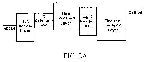
BRIEF DESCRIPTION OF DRAWINGS
Figures 1A-1B show a schematic energy diagram of a prior art infrared-to-green
light
up-conversion device without any charge blocking layer, where Figure 1A shows
the
schematic energy band diagram under no applied voltage in the dark and Figure
IB shows the
schematic energy band diagram even under low applied voltage in the dark.
Figures 2A-2C show a schematic energy band diagram of an IR-to-green light up-
conversion device with hole blocking layer according to an embodiment of the
invention,
where Figure 2A shows the schematic energy band diagram under no applied
voltage in the
CA 02800549 2012-11-22
WO 2011/149960 PCT/US2011/037772
3
dark, Figure 2B shows the schematic energy band diagram even under high
applied voltage in
the dark, and Figure 2C shows the schematic energy band diagram under applied
voltage in
the IR irradiation.
Figures 3A-3B show (3A) I-V characteristics and (3B) L-V characteristics of IR-
to-
green light up-conversion devices with various organic hole blocking layers
according to
embodiments of the invention with BCP and UGH2 as hole blocking materials
under dark
and IR irradiation.
Figures 4A-4B show (4A) I-V characteristics and (4B) L-V characteristics of IR-
to-
green light up-conversion devices with inorganic ZnO hole blocking layers
according to
embodiments of the invention compared with a device having an organic BCP hole
blocking
layer according to an embodiment of the invention under dark and IR
irradiation.
Figures 5A-5B show (5A) a schematic energy band diagram and (5B) L-I-V
characteristics of a QD based IR-to-visible light up-conversion device without
any charge
blocking layer under dark and IR irradiation.
Figures 6A-6C show (6A) a schematic energy band diagram, (6B) I-V
characteristics,
and (6C) L-V characteristics of a QD based IR-to-visible light up-conversion
device with
ZnO hole blocking layer according to an embodiment of the invention under dark
and IR
irradiation.
DETAILED DISCLOSURE
High-efficiency organic light-emitting devices, such as organic light-emitting
diodes
(OLEDs) and high efficiency organic photodetectors, have been demonstrated and
an all
organic up-conversion device has been disclosed by the inventors where an OLED
and an IR
photodetector are integrated into one device. (see Kim et at., PCT Patent
Application No.
PCT/US2010/058015, filed November 24, 2010 and Kim et at, Adv. Mater. 2010,
22, 2260-3,
both of which are hereby incorporated by reference herein in their entirety
and, in. particular,
are incorporated for their teachings of organic photodetectors and all organic
up-conversion
devices, for example, an organic light-emitting device, such as an OLED, and
an IR
photodetector integrated into one device). Because of their compatibility with
lightweight
rugged flexible plastic substrates, an all organic up-conversion device can
permit applications
unavailable to other more conventional technologies. Unfortunately, even in
the absence of
IR irradiation, an off state, organic up-conversion device can still give off
visible light, due to
CA 02800549 2012-11-22
WO 2011/149960 PCT/US2011/037772
4
the small difference between the work function of the anode and the highest
occupied
molecular orbit (HOMO) of the IR absorbing photodetector at low voltages.
Embodiments of the invention are directed to improved infrared imaging devices
where emission results from the up-conversion of an iR photodetector coupled
with an
organic light-emitting device, such as an OLED, where emission of light occurs
only under
IR irradiation at a sufficiently high voltage. Other embodiments of the
invention are directed
to a method of fabrication that is relatively low in cost and yields
lightweight, highly
sensitive devices with high gain and image fidelity while consuming little
power. Specific
embodiments can incorporate one or more of the organic IR-to-green light up-
conversion
devices disclosed in Kim et at., PCT/US2010/058015, or Kim et at. Adv. Mater.
2010, 22,
2260-3, where, in an exemplary embodiment, a tin phthalocyanine:
buckminsterfullerene
(SnPc:C60) bulk heterostructure layer IR photodetector is connected in series
with an fac-
tris(2-phenylpyridine)iridium (Ir(ppy)3) based phosphorescent layer as a light
emitting layer,
where the structure can be generalized by the structure diagrammed in Figure
IA, which is
similar to a conventional OLED.
In an all-organic up-conversion device, it can be advantageous to have a poor
hole
transport IR-sensitizing layer such that the organic light-emitting device,
such as an OLED,
remains in the off state until IR irradiation occurs. Upon IR photo-
excitation, holes are
injected into the organic light emitting layer where the holes combine with
electrons injected
from the cathode to give off light of a shorter wavelength than the incident
IR radiation, such
as visible light. As in the case of a device with an indium-tin oxide (ITO)
anode and IR
detecting (absorbing) tin (II) phthalocyanine (SnPc) layer, due to the small
difference
between the anode's work function and the IR absorber's HOMO, hole injection
from the
anode occurs at low voltages, as illustrated in Figure 1B. Hence, light can be
generated, even
with very little or no IR irradiation, with relatively low voltages applied to
the electrodes.
In embodiments of the invention, the performance of an all organic up-
conversion
device is enhanced by inclusion of a charge blocking layer. In a specific
embodiment, a hole
blocking layer is placed between an ITO anode and a SnPe IR photodetecting
layer, such that
hole carriers from the ITO anode are efficiently blocked, suppressing visible
luminance of the
up-conversion device until a sufficiently high voltages and IR irradiation is
applied, as shown
in Figures 2A, 2B, and 2C. In addition to ITO, other materials that can be
employed as an
anode include, but are not limited to: Indium Zinc Oxide (IZO), Aluminum Tin
Oxide (ATO),
CA 02800549 2012-11-22
WO 2011/149960 PCT/US2011/037772
Aluminum Zinc Oxide (AZO), and carbon nanotube. In addition to SnPc:C60, other
organic
IR photodetector materials that can be employed include, but are not limited
to: tin (11)
phthalocyanine (SnPc), aluminum phthalocyanine chloride (A1PcC1), AIPcCl:C60,
titanyl
phthalocyanine (TiOPc), and TiOPc:C60. In addition to Ir(ppy)3, other
electrohuninescent
5 organic light-emitting device, such as an OLED, materials that can be
employed include, but
are not limited to: poly-[2-methoxy, 5-(2'-ethyl-hexyloxy) phenylene vinylene]
(MEH-PPV),
tris-(8-hydroxy quinoline) aluminum (A1g3), and iridium (III) bis[(4,6-di-
fluorophenyl)-
pyridinate-N,C2']picolinate (FIrpie). The cathode can be LiF/Al or can be any
conductor
with the appropriate work function including, but not limited to: Ag, Ca:Mg,
LiF/Al/ITO,
Ag/ITO, CsCO3/ITO, and Ba/Al. Materials that can be employed as electron
transport layers
include, but are not limited to: tris[3-(3-pyridyl)-mesityl]borane (3TPYMB),
2,9-Dimethyl-
4,7-diphenyl-1,10-phenanthroline (BCP), 4,7-diphenyl-1,10-phenanthroline
(BPhen), and
tris-(8-hydroxy quinoline) aluminum (Alg3). Materials that can be employed as
hole
transport layers include, but are not limited to: 1,1-bis[(di-4-
tolylamino)phenyl]cyclohexane
(TAPC), N,N'-diphenyl-N,N'(2-naphthyl)-(1,1'-phenyl)-4,4'-diamine (NPB), and
N,N'-
diphenyl-N,N'-di(m-tolyl) benzidine (TPD). Those skilled in the art can
readily identify
appropriate combinations of anodes, cathodes, IR photodetectors, organic light-
emitting
device, such as OLED, materials, hole transport layers, and electron transport
layers by their
relative work functions, highest occupied molecular orbit (HOMO) and lowest
unoccupied
molecular orbit (LUMO) levels, layer compatibility, and the nature of any
desired deposition
methods used during their fabrication.
In some embodiments of the invention the hole blocking layer can be an organic
compound. Figure 3A shows I-V characteristics, and Figure 3B shows L-V
characteristics, of
IR-to-green light up-conversion devices according to embodiments of the
invention
fabricated with different organic hole blocking layers, 2,9-Dimethyl-4,7-
diphenyl-1,10-
phenanthroline (BCP) and p-bis(triphenylsilyly)benzene (UGH2), under dark and
IR
irradiation. These hole blocking materials possess deep HOMO levels. Because
these
materials also have small LUMO energy, charge generation between the hole
blocking layer
and the IR sensitizing layer is negligible. As illustrated in Figures 3A and
3B, up-conversion
devices with a hole blocking layer have higher turn-on voltage in the dark. In
addition to
BCP and UGH2, other organic hole blocking layers that can be employed in
embodiments of
the invention include, but are not limited to: 4,7-diphenyl-1,10-
phenanthroline (BPhen), tris-
CA 02800549 2012-11-22
WO 2011/149960 PCT/US2011/037772
6
(8-hydroxy quinoline) aluminum (A1g3), 3,5'-N,N'-dicarbazole-benzene (rCP),
C60, and
tris[3-(3-pyridyl)-mesityl]borane (3TPYMB).
In other embodiments of the invention an inorganic hole blocking layer can be
included in the up-conversion device. Figure 4A shows the I-V characteristics
and Figure 4B
shows the L-V characteristics of IR-to-green light up-conversion devices with
differing
thicknesses of ZnO hole blocking layers and, for comparison, a device with the
organic BCP
hole blocking layer under dark conditions and under IR irradiation. Devices
with ZnO hole
blocking layers display similar characteristics to that of BCP. In addition to
ZnO, other
inorganic hole blocking layers that can be employed in embodiments of the
invention include,
but are not limited to: Ti02, SiO, Si02, Si3N4, and A1703.
In another embodiment of the invention, the IR photodetecting layer can be
inorganic,
for example quantum dots (QDs) and the hole blocking layer can be organic or
inorganic.
For an exemplary up-conversion device lacking a hole blocking layer, shown in
Figure 5A, a
layer of PbSe QDs is employed as the IR sensitizer and MEH-PPV is employed as
the
electroluminescent organic light-emitting device, such as an OLED. The device
of Figure 5A
displayed no hole blocking by the QD IR detecting layer, as shown in Figure
513 where the L-
I-V characteristics on the QD IR up-conversion device displays little
difference between dark
and JR irradiated current densities and luminance with applied voltage, with
luminescence
occurring at a low voltage. In contrast, a QD IR up-conversion device with a
ZnO hole
blocking layer, as shown in Figure 6A, effectively blocks hole injection from
the anode in the
dark. This is shown by the I-V and L-V characteristics in Figures 6B and 6C
for a QD IR up-
conversion device with a ZnO hole blocking layer. In this embodiment, IR
irradiation acts as
an effective optical switch. In addition to PbSe, other QDs that can be
employed include, but
are not limited to: PbS. Other inorganic materials that can be employed as IR
detectors
include, but are not limited to: Si, Ge, and GaAs.
Embodiments of the invention pertain to methods and apparatus for detecting
infrared
(IR) radiation and providing an output having a shorter wavelength than the
incident IR
radiation, such as a visible light output. Because of their compatibility with
lightweight
rugged flexible plastic substrates, up-conversion devices in accordance with
embodiments of
the present invention can be used as a component, for example a pixel, for
numerous
applications including, but not limited to, night vision, range finding,
security, and
semiconductor wafer inspections.
CA 02800549 2012-11-22
WO 2011/149960 PCT/US2011/037772
7
All patents, patent applications, provisional applications, and publications
referred to
or cited herein are incorporated by reference in their entirety, including all
figures and tables,
to the extent they are not inconsistent with the explicit teachings of this
specification.
It should be understood that the examples and embodiments described herein are
for
illustrative purposes only and that various modifications or changes in light
thereof will be
suggested to persons skilled in the art and are to be included within the
spirit and purview of
this application.