Note: Descriptions are shown in the official language in which they were submitted.
CA 02801261 2012-11-30
PATENT APPLICATION
REF 27658/008WO1
Photovoltaic component for use under concentrated solar flux
PRIOR ART
Technical field of the invention
The present invention relates to a photovoltaic component for use under a
concentrated
solar flux, and to its manufacturing process, and especially relates to the
field of thin-film
photovoltaic cells.
Prior art
In the field of solar cells, those based on thin films are currently the focus
of intense
activity, to the detriment of the crystalline silicon traditionally used. This
industrial tendency
is mainly due to the fact that these films, smaller than 20 .im in thickness
and typically
smaller than 5 m in thickness, have an absorption coefficient for solar light
several orders of
magnitude higher than that of crystalline silicon, and to the fact that they
are produced
directly from gas and liquid phases and thus do not need to be sawn. Thus, a
thin-film
photovoltaic module may be produced with a film 100 times thinner than a
crystalline
photovoltaic cell. As a result, the expected costs are much lower, the
availability of raw
materials is increased, and the process for manufacturing the modules is
simpler. The main
technologies being developed at the present time are polycrystalline
chalcogenide
technologies, and especially CdTe technology and what is called chalcopyrite
technology
based on the compound CuInSe2 or its variants Cu(In, Ga)(S, Se)2, also called
CIGS, and
amorphous and microcrystalline silicon technologies.
Thin-film solar cells, especially those based on chalcopyrite materials such
as Cu(In,
Ga)Se2 or CdTe, have, at the present time, achieved laboratory efficiencies of
20% and
16.5%, respectively, under one sun illumination (i.e. 1000 W/m2). However, the
materials
used to manufacture solar cells are sometimes limited in their availability
(indium or
tellurium, for example). In the context of the development of photovoltaic
power stations with
capacities of the order of several GW, problems with the availability of raw
materials will
possibly become a major constraint.
I
CA 02801261 2012-11-30
PATENT APPLICATION
REF 27658/008WO1
Recently, concentrated photovoltaics (CPV) technology has been undergoing
development; this technology uses photovoltaic cells under a concentrated
solar flux.
Concentration of light allows the conversion efficiency of the cell to be
increased and
therefore raw material can be saved by a factor greater than the light
concentration employed,
for a given electricity production. This is of particular importance in thin-
film technologies.
Trials under concentration have demonstrated that efficiencies of 21.5% can be
obtained
under low concentration (14 suns, i.e. 14 times the average luminous power
received by the
Earth from the sun) if the frontside collecting grid has been optimized (see,
for example, J.
Ward et al. "Cu(In,Ga)Se2 Thin film concentrator Solar Cells", Progress in
Photovoltaics 10,
41-46, 2002). Above this concentration, dissipative effects due to the
resistance of the
collecting layer become too great for efficiency to be improved whatever the
design of the
frontside collecting grid, which, moreover, shades the cell (as much as 16%
being shaded).
Concentrator photovoltaics, though experiencing rapid growth at the present
time, thus remain
limited to simple 111-V semiconductor junction or multijunction cells, which
are very costly.
One object of the invention is to produce a photovoltaic cell that works under
a very
high concentration with a substantial reduction in the adverse effects of the
resistance of the
frontside layer. To do this, an innovative architecture has been developed,
especially allowing
arrays of microcells with contacts on their periphery to be produced, thereby
making it
possible to dispense with the use of a collecting grid. This architecture is
compatible with
existing solar cell technologies, especially thin-film technologies, and could
enable a
considerable saving in the use of rare chemical elements (indium, tellurium,
gallium).
SUMMARY OF THE INVENTION
According to a first aspect, the invention relates to a photovoltaic component
comprising:
- a set of layers suitable for producing a photovoltaic device, including at
least
one first layer made of a conductive material forming a back electrical
contact,
a second layer made of a material that is absorbent in the solar spectrum, and
a
third layer made of a transparent conductive material forming a front
electrical
contact;
- an electrically insulating layer, arranged between said back electrical
contact
and said front electrical contact, containing a plurality of apertures, each
2
CA 02801261 2012-11-30
PATENT APPLICATION
REF 27658/008WO1
aperture defining a zone in which said layers of said set of layers are
stacked to
form a photovoltaic microcell; and
a layer made of a conductive material, making electrical contact with said
third
layer made of a transparent conductive material, forming the front electrical
contact with said third layer, and structured in such a way as to form a
peripheral electrical contact for each of said photovoltaic microcells formed,
said microcells being electrically connected in parallel by the back
electrical
contact and the front electrical contact.
For example, said conductive material forming the layer made of a conductive
material
making electrical contact with said third layer made of a transparent
conductive material is a
metal chosen from aluminum, molybdenum, copper, nickel, gold, silver, carbon
and carbon
derivatives, platinum, tantalum and titanium.
According to one embodiment, the first layer made of a conductive material of
the back
contact is transparent, and the back contact further comprises a layer made of
a conductive
material making electrical contact with said layer made of a transparent
conductive material
structured in such a way as to form a peripheral electrical contact for said
photovoltaic
microcells.
According to another embodiment, the insulating layer comprises a layer made
of an
insulating material structured in such a way as to form a plurality of
apertures.
According to another embodiment, the photovoltaic component according to the
first
aspect further comprises a second layer made of an insulating material, said
layer being
arranged between said back electrical contact and said front electrical
contact, and being
structured in such a way as to form a plurality of apertures centered on said
apertures in the
first layer made of insulating material, and of equal or smaller size.
For example, said insulating material is chosen from oxides such as silica or
alumina,
nitrides such as silicon nitride, and sulfides such as zinc sulfide.
Alternatively, the insulating layer comprises an insulating gas, for example
air.
According to one preferred embodiment of the invention, at least one dimension
of the
section of the photovoltaic microcells is smaller than 1 mm and preferably
smaller than 100
m.
According to another embodiment, at least some of the photovoltaic microcells
have a
circular section with an area smaller than 10"2 cm2 and preferably smaller
than 10-4 cm2.
3
CA 02801261 2012-11-30
= PATENT APPLICATION
REF 27658/008WO1
According to another embodiment, the photovoltaic component according to the
first
aspect comprises at least one photovoltaic microcell with a strip-shaped
elongate section, the
smaller dimension of which is smaller than 1 mm and preferably smaller than
100 m.
According to another embodiment, the layer made of an absorbent material is
discontinuous and formed in the location of the photovoltaic microcells.
According to another preferred embodiment of the invention, the photovoltaic
component is a thin-layer component, each of the layers forming the cell
having a thickness of
less than about 20 m and preferably of less than 5 m.
For example, the absorbent material belongs to a family chosen from the CIGS
family,
the CdTe family, the silicon family, and the 111-V semiconductor family.
According to a second aspect, the invention relates to an array of
photovoltaic
components according to the first aspect, in which said photovoltaic
components are
electrically connected in series, the front contact of one photovoltaic
component being
electrically connected to the back contact of the adjacent photovoltaic
component.
According to a third aspect, the invention relates to a photovoltaic module
comprising
one or an array of photovoltaic components according to the first or second
aspect, and further
comprising a system for concentrating solar light, this system being suitable
for focusing all
or some of the incident light on each of said photovoltaic microcells.
According to one embodiment, the photovoltaic module according to the third
aspect
further comprises an element for converting the wavelength of the incident
light to a spectral
band absorbed by the absorbent material arranged under said first layer made
of a transparent
conductive material of the back contact, the back electrical contact
comprising a layer made
of a transparent conductive material and a layer made of a conductive
material, and the latter
layer being structured in such a way as to form a peripheral electrical
contact for said
photovoltaic microcells.
According to a fourth aspect, the invention relates to a method for
manufacturing a
photovoltaic component according to the first aspect, which method comprises
depositing said
layers forming the component on a substrate.
According to one embodiment, the manufacturing method comprises:
- depositing said first layer made of a conductive material on a substrate so
as to
form the back electrical contact;
4
CA 02801261 2012-11-30
PATENT APPLICATION
REF 27658/008WO1
- depositing a layer made of a material that is inactive with respect to the
photovoltaic device, preferably an electrical insulator, said inactive layer
being
structured to form a plurality of apertures;
- selectively depositing the absorbent material in said apertures so as to
form
said second layer made of an absorbent material, said layer being
discontinuous;
- depositing said layer made of a conductive material, said layer being
structured
in such a way as to form apertures of smaller or equal sizes to those of the
apertures in said inactive layer; and
- depositing said third layer made of a transparent conductive material making
electrical contact with said layer made of a conductive material, the latter
layer
being structured so as to form the front electrical contact.
According to another embodiment, the manufacturing method comprises:
- depositing said first layer made of a conductive material on a substrate so
as to
form the back electrical contact;
- depositing said second layer made of an absorbent material, said layer being
discontinuous and containing a plurality of apertures;
- selectively depositing in said apertures a material that is inactive with
respect
to the photovoltaic device, preferably an electrical insulator, so as to form
a
discontinuous inactive layer having apertures in the location of the absorbent
material;
- depositing said layer made of a conductive material, this layer being
structured
in such a way as to form apertures of smaller or equal sizes to those of the
apertures in said inactive layer; and
- depositing said third layer made of a transparent conductive material, this
layer
making electrical contact with said layer made of a conductive material, the
latter layer being structured to form the front electrical contact.
According to another embodiment, the manufacturing method comprises:
- depositing, on a substrate, said first layer made of a conductive material
so as
to form the back electrical contact, and said second layer made of an
absorbent
material;
- depositing a layer of resist structured to form one or more pads the shape
of
which will define the shape of each of the photovoltaic microcells;
5
CA 02801261 2012-11-30
PATENT APPLICATION
REF 27658/008W01
- depositing on said resist layer a layer made of an insulating material and a
layer made of a conductive material; and
- lifting off the resist in order to obtain said structured layer made of an
insulating material and said structured layer made of a conductive material,
and depositing said third layer made of a transparent conductive material,
this
layer making electrical contact with said structured layer made of a
conductive
material, so as to form the front electrical contact.
According to another embodiment, the manufacturing method comprises:
- depositing said third layer made of a transparent conductive material on a
transparent substrate so as to form the front electrical contact;
- depositing a layer of resist structured to form a plurality of pads the
shape of
which will define the shape of each of said photovoltaic microcells;
- depositing on said resist layer a layer made of a conductive material and a
layer made of an insulating material;
- lifting off the resist in order to obtain said structured layer made of an
insulating material and said structured layer made of a conductive material,
and depositing the layer made of an absorbent material; and
- depositing said first layer made of a conductive material so as to form the
back
electrical contact.
Advantageously, said layer made of an absorbent material is formed
selectively, and
forms a discontinuous layer.
BRIEF DESCRIPTION OF THE DRAWINGS
Other advantages and features of the invention will become apparent on reading
the
description, which is illustrated by the following figures:
- figures IA to I C are diagrams showing the principle of microcells according
to the
invention in various embodiments;
- figure 2 is a diagram illustrating the series connection of two islands each
comprising
an array of microcells according to the invention;
6
CA 02801261 2012-11-30
PATENT APPLICATION
REF 27658/008WOI
- figures 3A to 3D are diagrams illustrating set of layers for forming cells
according to
the invention in various embodiments;
- figures 4A to 4D are diagrams illustrating embodiments of cells according to
the
invention in the case of a CIGS, CdTe, amorphous silicon and crystalline
silicon
junction, respectively;
- figures 5A to 5F are diagrams illustrating, according to one embodiment, the
method
for manufacturing an island of microcells according to the invention, in the
case of a
CIGS-type junction;
- figure 6 is a curve illustrating the efficiency evaluated for a solar cell
according to one
embodiment of the invention, as a function of the incident power;
- figure 7 is a curve illustrating the efficiency evaluated for the solar cell
according to
the embodiment shown in figure 6, as a function of the area of the active zone
of the
cell; and
- figures 8A and 8B are micrographs of a microcell produced according to an
embodiment of the process according to the invention.
DETAILED DESCRIPTION
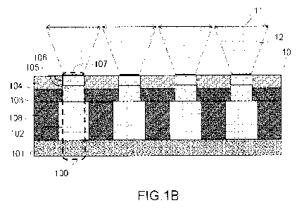
Figures IA to IC are diagrams showing the principle of photovoltaic modules
with
photovoltaic cells according to various embodiments of the present invention.
These diagrams
are by given way of illustration and the dimensions shown do not correspond to
the actual
scale of the cells.
These embodiments show a photovoltaic component 10 forming an island or an
array of
photovoltaic microcells or active photovoltaic zones 100 having an area 107 to
be exposed to
incident solar light and of given size and shape such that at least one
dimension of the
exposed area is smaller than a few hundred microns and advantageously smaller
than about
100 m. The microcells are associated with a system for concentrating solar
light (symbolized
in the figures by the microlenses 11) concentrating all or some of the solar
light incident on
each of the areas 107 of the microcells 100 (light flux indicated by the
reference 12).
7
CA 02801261 2012-11-30
PATENT APPLICATION
REF 27658/008WO1
Each microcell comprises a set of layers suitable for producing a photovoltaic
device,
especially with a layer 102 made of a material that is absorbent in the
visible spectrum or
near-infrared (solar spectral range), or in part of the solar spectrum; a
layer 101 of a
conductive material forming a back electrical contact; and a layer 106 of a
transparent
conductive material, covering the exposed area 107, forming a front electrical
contact, the
layer 106 also being called a window layer. Depending on the nature of the
photovoltaic
device that it is desired to produce, one or more additional layers 105 may be
provided, for
example layers made of semiconductors or interface layers that, with the layer
102 made of an
absorbent material, will contribute to form a junction. In figures IA, 1B, and
1C the front
electric contact is formed by the layers 104, 106, as will be described in
more detail below. In
the embodiments in figures I A to I C, the microcells 100 are connected in
parallel both by the
front electrical contact (106 and/or 104) and the back electrical contact 101,
the front and
back contacts being common to all the microcells.
According to one embodiment, the system for concentrating light allows light
having a
spectrum suited to the absorption range of the absorbent material of said
microcell to be
focused on each microcell.
The island 10 comprises an electrically insulating layer 103 arranged between
the back
electrical contact and the front electrical contact. The insulating layer 103
is discontinuous so
as to form one or more apertures that define the shape and the dimensions of
the microcells or
active photovoltaic zones 100 of the island 10. Beyond these apertures, dark
current densities
are actually negligible. In the apertures, the junction is formed by the set
of semiconductor
layers. The front and back electrical contacts allow photogenerated charge
carriers to be
collected. Thus, by choosing the dimensions of the microcells (the sections of
which are
defined by the apertures formed in the insulating layer) such that at least
one dimension of a
section of the microcell is smaller than a few hundred microns, the Applicants
have
demonstrated that charge carriers photogenerated in each microcell can be
collected by virtue
of the front electrical contact while losses due to the resistance of the
transparent conductive
layer contributing to this contact are limited. The array thus formed forms a
solar cell suited
to an application under concentrated solar flux, which does not require the
use of a collecting
grid. The Applicants have demonstrated that, by virtue of this novel
structure, theoretical
efficiencies of 30% could be achieved under concentrations of more than 40,000
suns for cells
in which the efficiency is 20% without concentration, considerably exceeding
the
concentration limits proposed until now in prior-art embodiments.
8
CA 02801261 2012-11-30
PATENT APPLICATION
REF 27658/008WO1
In figures I A to IC, the microcells 100 for example have a round section,
advantageously with an area smaller than 10-2 cm2, even smaller than 10-4 cm2,
and down to
as low as 10-8 cm2 or less, so as to enable rapid collection of charge
carriers. The lower limit
of the area is linked to technological considerations and to the mobility and
lifetime properties
of the carriers photogenerated in the layer of absorbent material.
The insulator may be a layer formed from an electrically insulating material
pierced
with apertures, such as an oxide such as silica (Si02) or alumina (A1203), a
nitride, for
example silicon nitride (Si3N4), a sulfide, for example zinc sulfide (ZnS), or
any other
insulating material compatible with the process for manufacturing the cell,
for example a
polymer. The insulator may also be a layer of gas, for example of air, for
example contained
in a porous or cellular material, or taking the form of a foam, depending on
the process
technology used to manufacture the component. The layer of gas, for example
air, is then
interrupted in zones where layers, including the layer formed by the porous
material, are
stacked to form the active photovoltaic zones. For example, it may be
envisioned, in a silicon-
based photovoltaic cell, to use a layer made of recrystallized porous silicon,
in which the air
bubbles formed during the anneal form the discontinuous insulating layer, the
silicon forming
the active photoconductive layer.
The section defines the area 107 of the active photovoltaic zones exposed to
incident
light and the system 1 l for concentrating light will have to be modified to
focus incident light
onto the exposed areas of the microcells. For example, in the case of
microcells with a
circular section, a system comprising a network of microlenses will possibly
be used, or any
other known system for focusing light. The system for concentrating light is
tailored to the
dimensions of the illumination areas, and will itself have a smaller volume
than that of a
concentrating system used with a conventional cell. This has the additional
advantage that less
material is used to produce the system for concentrating light.
The section of the microcells may take various shapes. For example, it is
possible to
envision a section of elongate shape, for example a strip, with a very small
transverse
dimension, typically smaller than one millimeter and advantageously smaller
than one
hundred microns and even as small as a few microns or less. The charge
carriers
photogenerated at the junction may then be collected via the front contact
along the smaller
dimension of the strip, once more allowing the resistance effects of the
window layer formed
by the layer made of a transparent conductive material of the front contact to
be limited. In
this case, the system for concentrating light will be modified in order to
focus one or more
9
CA 02801261 2012-11-30
PATENT APPLICATION
REF 27658/008WO1
lines, following the structure of the island, on one or more strips. If the
island comprises a
plurality of strips, these strips will possibly be electrically connected in
parallel both by the
back contact and the front contact. Other shapes can be envisioned, such as
for example an
elongate serpentine shape, etc., providing that one of the dimensions of the
section is kept
small, typically smaller than a few hundred microns, for collection of charge
carriers. In
particular, the dimensions will possibly be optimized depending on the
materials used,
especially to minimize the influence of lateral electrical recombination.
Charge carriers generated in the layer 102 in the active zone bounded by the
exposed
area 107 are collected via the layer 106 made of a transparent conductive
material or window
layer, firstly in the direction perpendicular to the plane of the layers, then
towards the
periphery of the microcell. This layer must be sufficiently transparent to
allow as much solar
light as possible to penetrate into the active photovoltaic zone 100. It
therefore has a certain
resistivity, possibly leading to losses, but the effect of this will be
limited by the size of the
microcell.
The Applicants have demonstrated that peripheral charge-carrier collection is
greatly
improved by associating, with the window layer, a layer 104 made of a
conductive material,
making electrical contact with the window layer 106, the assembly of the two
layers then
forming the front contact. The layer 104 made of a conductive material is for
example made
of metal, for example of gold, silver, aluminum, molybdenum, copper, or
nickel, depending
on the nature of the layers to be stacked, or made of a doped semiconductor,
for example
ZnO:Al, sufficiently doped with aluminum to obtain the desired conductivity.
Like the
insulating layer 103, the layer 104 made of a conductive material is
discontinuous, pierced
with apertures that may be substantially superposed on those of the insulating
layer so as not
to interfere with the photovoltaic function of the microcell 100. The charge
carriers
photogenerated in the active layer 102 in the active zone are collected in the
direction
perpendicular to the plane of the layers by virtue of the window layer 106,
then collection
toward the periphery of the microcell is enabled by the conductive layer 104
which thus forms
a peripheral contact of the microcell.
The layer 104 forming the peripheral contact of the microcells may completely
cover the
area between the microcells, or may be structured in such a way as to have
peripheral contact
zones with each of the microcells and electrical connection zones between
said, non-
overlapping, peripheral contact zones.
CA 02801261 2012-11-30
PATENT APPLICATION
REF 27658/008WO1
Since the active photovoltaic zones of the cell 10 are set by the dimensions
of the one or
more apertures in the insulating layer, so as to form microcells, it is
possible to limit the
amount of material in the layers forming the photovoltaic device, and
especially the amount
of absorbing material. Thus, in the embodiment in figure 113, the absorbent
layer 102 is
discontinuous and limited to zones located in the active zones 107. The rest
of the structure
may be filled with a layer 108 that is inactive from the point of view of the
junction, this layer
possibly being an insulator, made of the same material as the layer 103.
Advantageously, the
zone comprising the absorbent material is slightly larger than the active
photovoltaic zone
defined by the aperture in the insulating layer 103 (typically a few microns),
thus making it
possible to marginalize the influence, on the photovoltaic microcell, of
surface defects
possibly related to the material itself or to the manufacturing process.
Figure 1 C shows an embodiment in which the layer 101 made of a conductive
material
is transparent and the back contact is formed, as the front contact (104A,
106), from the layer
101 and a layer 104B made of a conductive material, for example a metal, the
layer 104B being
structured, like the layer 104A, in such a way as to form a peripheral
electrical contact for the
active photovoltaic zones. This variant has the advantage of providing a back
contact with a
transparent window layer, thus forming bifacial cells, this being made
possible by the
peripheral collection of charge carriers and the limitation of losses due to
the resistance of the
transparent window layer even under concentration. This enables various
applications, such as
for example the production of multijunctions in which two or more photovoltaic
cells are
superposed on one another. Or, according to another embodiment, it allows the
photovoltaic
cell to be associated with a device for converting light, arranged under the
window layer of
the back contact, this device reflecting light that is not absorbed during a
first passage through
the cell (for example light in the near infrared) back toward the cell, this
light having its
wavelength modified (for example shifted toward the visible range, or more
generally into the
spectral range more readily absorbed by the absorbent material, using an "up
conversion"
material).
Figure I C shows another embodiment in which a second layer 103E made of an
insulating material is provided, structured substantially identically to the
first layer 103A made
of an insulating material, with one or more apertures centered on the one or
more apertures of
the layer 103A made of an insulating material, and of equal or smaller size.
This second layer
may for example have the effect of concentrating lines of current into an
active photovoltaic
volume.
11
CA 02801261 2012-11-30
PATENT APPLICATION
REF 27658/008WO1
According to one embodiment shown in figure 2, a plurality of islands (10A,
10B) may
be electrically connected to form a larger photovoltaic cell. The islands are
for example
formed on a common substrate 109. In figure 2, a single microcell 100 is shown
per island,
but, of course, each island may comprise a plurality of microcells. In this
embodiment, as in
that in figures ]A and 113, the front electrical contact comprises a layer
(104A, 1048) made of
a conductive material and a window layer (I06A, 10613) that covers, in this
embodiment, all of
the island. In this embodiment, the islands are connected in series by means,
for example, of
the window layer 106A of the first island 10A, which makes electrical contact
with the back
electrical contact 10113 of the second island 108. It will be understood that
figure 2 is a
diagram showing an operating principle. It may be necessary, in the case where
the
conductivity of the layer 102A is high, to insulate the layer 106A, for
example by extending the
insulating layer 103A to level with where the islands are connected.
Figures 3A to 3D show diagrams illustrating the succession of layers used to
form cells
according to the invention in various embodiments. Several architectures for
producing thin-
layer microcells are presented here. In this technology, the photovoltaic
device comprises a
junction formed by means of n- and p-doped semiconductor layers, the
electrically insulating
layer 103 being interposed between said layers. In these embodiments, the
layers forming the
junction are the layers 102 (layer made of an absorbent material), 112
(representing one or
more interface layers) and 106 (which forms the transparent window layer).
Structuring the
insulating layer makes it possible to create disks 301 of controlled area in
which this layer is
not deposited. The insulating layer allows circular photovoltaic cells to be
defined since the p-
n or n-p semiconductor junction will only be formed in the disks. The
electrically conductive
layer 104, for example made of a metal, structured in a similar way to the
insulating layer
(comprising circular holes 302), is arranged to make electrical contact with
the window layer
106 in order to form, with the window layer, the frontside contact (except in
the embodiment
in figure 3D where the layer 106 alone forms the front contact). Either the
conductive layer
104 is deposited on the insulating layer 103 (figure 3B), before the window
layer 106 has
been deposited, or it is deposited on the window layer (figure 3A). The
interface layers 112
may be deposited before the insulating layer (figures 3A, 3B) or after the
latter (figure 3C),
the electrical contact between the metallic layer and the window layer being
preserved if the
interface layer is sufficiently thin. The presence of interface layers having
a very low lateral
conductivity (intrinsic CdS and ZnO in the case of a CIGS cell, for example)
makes it
possible to ensure that the junction from the optical point of view, and the
junction from the
12
CA 02801261 2012-11-30
PATENT APPLICATION
REF 27658/008WO1
electrical point of view, are similar. Thus, the electrically active parts are
correctly excited by
incident light, while losses due to recombination of charge carriers and the
dark current of the
junction are minimized.
It is also possible to tailor this geometry to the case of superstrate cells
(figure 3D)
produced on a glass substrate 109 with what is called a "top to bottom"
process, such as will
be described below, and then flipped to allow incident light to enter via the
side
corresponding to the substrate.
As has been described above, the conductive layer 104, for example made of
metal,
makes it possible to produce an annular contact on the periphery of the
microcell and
common to all the microcells, this contact possibly being used directly as the
front electrical
contact of the cell, thereby minimizing contact resistances while avoiding
shading the cell
since no collecting grid is required. Interposing the layer 103 made of an
insulating material
structured with one or more apertures in the set of layers forming the
photovoltaic device is an
advantageous way in which to define the microcells, because this solution does
not require
mechanical etching of the set of layers, which is inevitably a source of
defects.
Figures 4A to 4D show four embodiments of cells according to the invention
using
CIGS, CdTe and silicon technologies, respectively. In each of these
embodiments, the entire
photovoltaic cell has not been shown, but only the set of layers in a
microcell. Here again,
these are illustrative diagrams in which the dimensions do not correspond to
the actual scale
of the cells.
Figure 4A shows a set of layers suitable for forming photovoltaic microcells
using a
CIGS-type heterojunction. The term "CIGS" is here understood in its most
general sense to
mean the family of materials including CuInSe2 or one of its alloys or
derivatives, in which
copper may be partially substituted by silver, indium may be partially
substituted by
aluminum or gallium, and selenium may be partially substituted by sulfur or
tellurium. The
natures of the materials are given above by way of example, and may be
substituted by any
other material known to a person skilled in the art to obtain a functional
photovoltaic device.
In the embodiment illustrated in figure 4A, the set of layers comprises a
substrate 109, for
example made of glass, the thickness of the substrate typically being a few
millimeters; and a
layer 101 made of a conductive material, for example of molybdenum, forming
the back
contact. The thickness of this layer is about one micron. The layer 102 is the
layer made of an
absorbent semiconductor material, in this embodiment Cu(In, Ga)Se2 (copper
indium gallium
diselenide). It is for example 2 or 3 m in thickness. The layers 110 and 111
are interface
13
CA 02801261 2012-11-30
PATENT APPLICATION
REF 27658/008WOI
layers, respectively made of n-doped CdS (cadmium sulfide) and iZnO (intrinsic
zinc oxide) a
few tens of nanometers, for example 50 nm, in thickness. Generally, the
interface layers allow
electrical defects present when the layer of absorbent material (here CIGS)
and the layer made
of a transparent conductive material make direct contact to be passivated,
these defects
possibly severely limiting the efficiency of the cells. Other materials may be
used to form an
interface layer, such as zinc-sulfide derivatives (Zn, Mg)(O, S) or indium
sulfide In2S3, for
example. The set of layers comprises the layer 103 made of an electrical
insulating material,
for example of Si02 (silica), structured so as to form the apertures allowing
the active
photovoltaic zone(s) to be defined. It is a few hundred nanometers, for
example 400 nm, in
thickness. The layer 104 is a layer made of a conductive material, for example
a metallic
layer, ensuring the peripheral contact of the microcell. It is structured
identically to the
insulating layer 103. It is a few hundred nanometers, for example 300 nm, in
thickness. It is
for example made of gold, copper, aluminum, platinum or nickel. It could also
be made of
highly aluminum-doped ZnO:Al. Finally, the layer 106, for example made of n-
doped ZnO:AI
(aluminum-doped zinc oxide), forms the front window layer and also contributes
to the
junction. It is also a few hundred nanometers, for example 400 nm, in
thickness. An
embodiment of a process for producing the structure 4A will be described in
greater detail by
way of figures 5A to 51.
Figure 4B shows a set of layers suitable for forming photovoltaic microcells
using a
CdTe-type heterojunction. The term "CdTe" is here understood in its most
general sense to
mean the family of materials including CdTe or one of its alloys or
derivatives, in which
cadmium may be partially substituted by zinc or mercury and tellurium may be
partially
substituted by selenium. Here again, the natures of the materials are given
above by way of
example. The set of layers comprises a layer 101 made of a conductive
material, for example
of gold or of a nickel/silver alloy, forming the back contact. This layer is
about one micron in
thickness. The layer 102 is the layer made of an absorbent material, in this
embodiment p-
doped CdTe (cadmium telluride). It is a few microns, for example 6 gm, in
thickness. An
interface layer 113 made of n-doped CdS is arranged between the CdTe layer and
the
insulating layer 103. It is about one hundred nanometers in thickness. The set
of layers
comprises the layer 103 made of an electrically insulating material, for
example of Si02,
structured to form apertures allowing the one or more active photovoltaic
zone(s) to be
defined. It is a few hundred nanometers, for example 400 nm, in thickness.
Next comes the
window layer 106 made of a transparent conductive material, for example of ITO
(indium tin
14
CA 02801261 2012-11-30
PATENT APPLICATION
REF 27658/008WO1
oxide) or of n-doped Sn02 (tin dioxide), which is a few hundred nanometers,
for example 400
nm, in thickness, and the layer 104 made of a metallic material ensuring the
peripheral contact
of the microcell, for example made of gold, and structured identically to the
insulating layer
103, and of a few hundred nanometers, for example 400 nm, in thickness. In
this embodiment,
the manufacturing process is a "top to bottom" process, and the substrate 109
is placed on the
side of the cell intended to receive incident solar light.
Figure 4C shows a set of layers suitable for forming photovoltaic microcells
using the
family of silicon thin layers comprising amorphous silicon, and/or
polymorphous,
microcrystalline, crystalline and nanocrystalline silicon. In the embodiment
in figure 4C, a
junction is formed by the layers 114, 115, and 116, respectively made of p-
doped amorphous
silicon, intrinsic amorphous silicon and n-doped amorphous silicon, these
layers together
being absorbent in the visible, the total thickness of the three layers being
about 2 m. The
layers forming the junction are arranged between the back electrical contact
101 (metallic
layer, for example made of aluminum or silver) and the structured insulating
layer 103, for
example made of Si02 and about a few hundred nanometers, for example 400 nm,
in
thickness. A front metallic layer 104, structured similarly to the insulating
layer and of
substantially the same thickness, is arranged on the latter, and on this front
metallic layer 104
the window layer 106 made of a transparent conductive material, for example
Sn02, is found,
the latter layer also being a few hundred nanometers in thickness. Again, in
this embodiment
the top to bottom process is used, the substrate being positioned on the side
of the cell
exposed to incident light.
Other families of absorbent materials may be used to produce a thin-layer
photovoltaic
cell according to the present invention. For example, III-V semiconductors
such as GaAs
(gallium arsenide), InP (indium phosphide) and GaSb (gallium antimonide) may
be used. In
any case, the nature of the layers used to form the photovoltaic device will
be tailored to the
device.
The last embodiment (figure 4D) illustrates implementation of the invention
using
crystalline silicon. Although the invention is particularly advantageous for
thin-layer
technologies, it is nevertheless also applicable to traditional crystalline-
silicon technology. In
this case, the layers 117 and 118, respectively made of p- (boron) doped
crystalline silicon
and n- (phosphorus) doped crystalline silicon, form a junction arranged
between the back
metal contact 101 and the insulating layer 103. In total, the junction is a
few hundred microns,
typically 250 m, in thickness, which makes this embodiment less attractive
than a thin-layer
CA 02801261 2012-11-30
PATENT APPLICATION
REF 27658/008WO1
embodiment and limits the possible reduction in the size of the microcell
(typically, the
minimum size here will be about 500 m, in order to limit the influence of
lateral
recombination). As in the preceding embodiment, the junction is covered with
the structured
insulating layer 103, with the layer 104 made of a conductive material
structured in the same
way, and with the window layer 106, which is for example made of Sn02. The
layers 103,
104, 106 are a few hundred nanometers, for example 400 nm, in thickness. A
substrate is not
required because of the thickness of the layers forming the junction. An
antireflection layer
119 may be provided in this embodiment, and also, more generally, in all the
embodiments.
Figures 5A to 5F illustrate, according to one embodiment, the steps of a
process for
manufacturing a photovoltaic cell with a CIGS junction of the type shown in
figure 4A.
In a first step (figure 5A), the basic structure is produced by depositing, in
succession,
on a substrate (not shown) the layer 101 made of a conductive material (for
example
molybdenum), the CIGS layer 102, and two interface layers 110, 111 made of CdS
and iZnO,
respectively. A partial top view of the basic structure is also shown. In a
second step (figure
513) a resist layer, for example consisting of circular pads 50 of a diameter
tailored to the size
of the microcell that it is desired to produce, is deposited. The resist pads
are produced, for
example, using a known lithography process, consisting in coating the sample
with a resist
layer, exposing the resist through a mask, and then soaking the sample in a
developer which
selectively dissolves the resist. If the photoresist used is a positive
resist, the part exposed will
be soluble in the developer, and the unexposed part will be insoluble. If the
photoresist used is
a negative resist, the unexposed part will be soluble and the exposed part
will be insoluble.
The resist used to manufacture the cells can be positive or negative,
irrespectively. Next, the
insulating layer 103 is deposited (figure 5C), and then the layer 104 made of
a conductive
material 104 is deposited (figure 5D). Next, the resist is dissolved (figure
5E) in order to
obtain layers 103 and 104 made of insulating and conductive materials
identically structured
with circular apertures exposing the surface of the upper layer of the
junction (commonly
known as "lift-off'). Next, the layer 106 made of a transparent conductive
material (for
example ZnO:Al) is deposited (figure 5F). In order to allow two of the islands
formed in this
way to be connected in series (as illustrated in figure 2), the layer 101 made
of a conductive
material may be partially exposed.
Figures 5A to 5F show an embodiment of what is called a "bottom to top"
process
suitable for a CIGS-type junction, a "bottom to top" process being a process
in which the
layers are deposited in succession on the substrate, from the lowest layer to
the highest layer
16
CA 02801261 2012-11-30
PATENT APPLICATION
REF 27658/008WO1
relative to the side exposed to incident light. In the case of CdTe-1 or
amorphous-silicon-type
junctions (figures 4B, 4C), a "top to bottom" process will be preferred, in
which the layers
that will be nearer the side exposed to incident light are deposited on the
substrate (generally a
glass substrate) first, the cell then being flipped when it comes to being
used. The choice of
whether a top to bottom process is used depends especially on how well the
materials
employed adhere to the substrate, and on how difficult it might be to make
"contact" to the
layer made of an absorbent material. Thus, a top to bottom process may
comprise: depositing
the layer 106 made of a transparent conductive material on a transparent
substrate 109 in
order to form the front electrical contact; depositing a resist layer
structured to form one or
more pads, the shape of which will define the shape of the active photovoltaic
zone(s);
depositing the layer 103 made of an insulating material on said resist layer;
lifting off the
resist layer; depositing the layer 102 made of an absorbent material; and
finally, depositing a
conductive layer on the photoconductive layer in order to form the back
contact. When the
front contact is formed by the layer 106 made of a transparent conductive
material and by a
structured layer 104 made of a conductive material, it is possible to deposit
the layer 104
made of conductive material on the resist layer and then to deposit the
insulating layer 103
before the resist has been dissolved. If, as in the embodiment shown in figure
4B, it is chosen
to insert a layer 106 made of a transparent conductive material between the
layer 104 made of
a conductive material and the insulating layer 103, it will be possible to
deposit the resist
pads, deposit the conductive material, dissolve the resist, deposit the layer
106 made of a
conductive transparent material, once more deposit resist, deposit the
insulating layer and then
dissolve the resist.
Moreover, to produce photovoltaic cells of the type shown in figure 113,
several
production methods may be considered.
According to a first embodiment, the layer 101 made of a conductive material
is
deposited on a substrate (not shown in figure IB) in order to form the back
electrical contact,
then the inactive layer 108, advantageously made of an insulating material, is
deposited, this
layer being structured to form one or more apertures. The absorbent material
is then
selectively deposited in the one or more apertures so as to form the layer 102
made of an
absorbent material, this layer being discontinuous. The selective deposition
is carried out
using a suitable method, for example electrodeposition or printing, for
example jet printing or
screen printing. Next, the layer 106 made of a transparent conductive material
is deposited in
order to form the front electrical contact. This step may be preceded by the
deposition of one
17
CA 02801261 2012-11-30
PATENT APPLICATION
REF 27658/008WO1
or more interface layers and/or of a structured layer 103 made of an
insulating material, if the
inactive layer 108 is not or not sufficiently insulating, and of the
structured layer 104 made of
a conductive material forming, with the transparent conductive layer 106, the
front electrical
contact.
In a second embodiment, the layer 102 made of an absorbent material is
deposited on
the layer 101 made of a conductive material, said absorbent layer being
discontinuous so as to
form one or more apertures, an inactive material, for example an insulating
material, then
being selectively deposited in the one or more apertures so as to form the
inactive layer 108.
The layer made of an absorbent material is, in this embodiment, deposited by
ink jet printing,
for example. As before, the layer 106 made of a transparent conductive
material is then
deposited to form the front electrical contact, this step optionally being
preceded by the
deposition of a structured layer 103 made of an insulating material, by the
deposition of one
or more interface layers, and by the deposition of the structured layer 104
made of a
conductive material.
According to a variant, the selective deposition of the absorbent material is
achieved by
depositing grains of the material, obtained using known techniques, for
example high-
temperature metallurgical synthesis methods, or by generating powders from
preliminary
vapor-phase deposition on intermediate substrates. CIGS grains of one to
several microns in
size may thus be prepared and deposited directly on the substrate in the
context of the
invention. Alternatively, all or some of the layers intended to form the
photovoltaic junction
may be stacked beforehand, in the form of solid panels, using conventional
techniques (for
example coevaporation or vacuum sputtering), then portions of the multilayer
stack, of
dimensions suited to the size of the microcells it is desired to produce, are
selectively
deposited on the substrate.
According to another variant, the selective deposition of the absorbent
material is
achieved using a physical or chemical vapor deposition method. To do this,
masks will
possibly be used, which masks will be placed directly in front of the
substrate, and in which
apertures are made in order to allow the selective deposition of the absorbent
layer and,
optionally, other active layers forming the junction on the substrate.
Coevaporation and
sputtering methods are examples of methods that may be used in this context.
Any one of these embodiments makes it possible, by virtue of the discontinuous
nature
of the layer of absorbent material obtained, to limit the amount of absorbent
material required
18
CA 02801261 2012-11-30
PATENT APPLICATION
REF 27658/008W01
to produce the photovoltaic cell, and therefore to make a substantial saving
in the amount of
rare chemical elements used.
Cells according to the invention may thus be produced using processes that
involve
merely depositing and structuring an electrically neutral layer and an
electrically conductive
layer. These two layers may very easily be composed of inexpensive and
environmentally
harmless materials (Si02 as the insulator and aluminum as the conductor, for
example). The
deposition techniques used (sputtering) are very commonplace and not
particularly hazardous.
The techniques employed are techniques used in the microelectronics industry
(UV
lithography) for example, the risks of which are limited in terms of toxicity
and which may
therefore be easily implemented. Scaling up to industrial-scale production may
therefore be
envisioned on the base of the know-how of the microelectronics industry.
Simulations carried out by the Applicant of the theoretical efficiency of the
photovoltaic
cells described above returned remarkable results. The model used is based on
electrical
analysis of a solar cell having a resistive front layer (window layer) with a
given sheet
resistance. The underlying equations of this model are, for example, described
in N. C. Wyeth
et al. Solid-State Electronics 20, 629-634 (1977) or U. Malm et al., Progress
in Photovoltaics,
16, 113-121 (2008). The Applicant studied the combined effect of light
concentration and
microcell size in an architecture such as that described above, for a
microcell with a circular
section, using an electrical contact method not employing a collecting grid.
The model is based entirely on the solution to the equation:
a2yi1arz +1/rxayr/ar+RII(Jph -Jõ(exp(gyi/nkT)-1)-W/R,.h)=0
where w is the electrical potential at a certain distance r from the center of
the cell, R[1 is
the sheet resistance of the front window layer, Jph is the photocurrent
density, J0 is the dark
current density, Rsh is the leakage resistance, n is the ideality factor of
the diode, k is
Boltzmann's constant, and q is the charge on an electron.
The boundary conditions allowing this equation to be solved are, in the case
of a
peripheral contact:
ye(a) = V where a is the radius of the cell and V the voltage applied to the
latter; and
ayr/ar(0) = 0 because no there is no current flow at the center of the cell
for reasons of
symmetry.
Figure 6 shows the efficiency curve calculated as a function of the incident
power
density (or concentration factor in units of suns) for various sheet
resistances of the window
layer ensuring the peripheral contact of the microcell. To carry out this
simulation, a microcell
19
CA 02801261 2012-11-30
PATENT APPLICATION
REF 27658/008WOI
of circular section was considered with a radius of 18 m (i.e. an area of
10"5 cm2) and the
electrical parameters of a CIGS-based reference cell (without light
concentration) were
employed, namely a short-circuit current Jsc = 35.5 mA/cm2, a diode ideality
factor of n =
1.14, and a dark current Jo = 2.1x10⁹ mA/cm2 (parameters evaluated, for
example, by
I.Repins et al., 33rd IEEE Photovoltaic Specialists Conference, 2008, 1 - 6
(2008), or I.Repins
et al., Progress in Photovoltaics 16, 235-239 (2008)).
The efficiency was calculated for three values of the sheet resistance R,h,
10, 100 and
1000 SZ/^, respectively, for luminous power varying between 10-4 and 104
W/cm2, i.e. a
concentration factor in units of suns varying between 10-3 and 105 (one sun
corresponding to
1000 W/m2, i.e. 10-1 W/cm2). Thus, for a sheet resistance of 1000 Q/^, the
efficiency
increases with concentration factor up to about 5000 suns, above which value
sheet resistance
effects reduce the efficiency. For sheet resistances lower than 100 Q/^, the
resistance is no
longer the main limiting factor in the calculation of the theoretical
efficiency of the cell and
efficiencies of about 30% are achieved with concentration factors approaching
50,000 suns.
This is noteworthy in that it is then possible to work with window layers
having a better
transparency (even if the resistance is higher) allowing larger photocurrents
to be generated.
Specifically, in the particular case of thin-layer cells for example, the use
of a frontside
transparent conductive oxide necessarily leads to a compromise between
transparency and
conductivity. Specifically, the higher the conductivity of the window layer,
the less it is
transparent. The geometry of the cell according to the inveniton, which
relaxes the constraint
on the conductivity of the window layer (because resistance effects are
rendered negligible),
allows very transparent layers to be used (even though the latter are more
resistive). An
increase in the photocurrent (i.e. the current generated by light incident on
the cell) of about
10% is expected since the window layer will absorb less of the incident light,
and thus the
absorbent part of the cell will receive more light.
Figure 7 illustrates, under the same calculation conditions as before, the
efficiency of the
microcell as a function of the area of the active photovoltaic zone for a
layer resistance of 10
ohms, the efficiency being given for the value of the optimal concentration
factor above
which the efficiency decreases. These values of the optimal concentration
factor are given for
4 microcell sizes. Thus, for a cell with a section of 10-1 cm2, under a
concentration of 16 suns,
the efficiency calculated was 22%. For a cell with a section of 10-2 cm2,
under a concentration
of 200 suns, the efficiency calculated was 24%. For a cell with a section of
10-3 cm2, under a
CA 02801261 2012-11-30
PATENT APPLICATION
REF 27658/008WO1
concentration of 2000 suns, the efficiency was 27%, and for a cell with a
section of 10-5 cm2,
under a concentration of 46,200 suns, the efficiency calculated was 31%. For
microcells with
sections smaller than 4.5X105 cm2, the optimal concentration factor was higher
than 46,200,
showing that sheet resistance was no longer a factor limiting the performance
of the
microcell.
As will be clear from the results presented, the novel architecture of the
photovoltaic
cell according to the invention especially allows the influence of the
resistance of the window
layer to be limited, and thus allows much higher concentrations to be used,
these
concentrations being associated with higher conversion efficiencies. Several
advantages are
obtained. Using microcells under a concentrated flux especially enables the
ratio of the
amount of raw material used to the energy produced to be reduced. A material
saving of a
factor higher than or equal to the light concentration is then possible. The
energy produced
per gram of raw material used could be multiplied by a factor of one hundred
or even several
thousand, depending on the light concentration employed. This is particularly
important for
materials such as indium, the availability of which is limited. Moreover,
under light
concentration, materials of average quality could be used without a
substantial decrease in
performance, since it is known that using a concentrated flux saturates
electrical defects in the
material. Saturation of these defects thus makes it possible to neutralize
their influence on the
performance of the cell. Very high efficiencies could therefore be obtained
using materials
which, without concentration, would remain substandard. This means, for
example, that
materials having a limited cost could be suitable for use under concentration.
The invention moreover uses the already tried-and-tested techniques of
microelectronics
to define the microcells, and it is therefore suitable for many existing
photovoltaic
technologies, even though, at the present time, the most promising
applications are expected
to be in the field of thin-layer cells.
The Applicants have produced prototype microcells using one embodiment of a
process
described in the present invention. Figures 8A and 8B show micrographs of a
CIGS-based
microcell as seen from above, respectively taken with an optical microscope
(figure 8A) and
with a scanning electron microscope (SEM) (figure 8B). The microcells were
produced using
the process described with reference to figures 5A to 5F, with round sections
having
diameters varying between 10 m and 500 m. The microcells shown in figures 8A
and 8B
are microcells with a diameter of 35 m. In these micrographs, the reference
106 indicates the
window layer made of ZnO:Al deposited on the layer 104, and the reference 107
indicates the
21
CA 02801261 2012-11-30
PATENT APPLICATION
REF 27658/008WOI
exposed area corresponding to the active photovoltaic zone. With these cells,
the Applicants
recorded very promising initial results, exhibiting the beneficial effect of
the size of the
microcell on the performance under concentration, without degradation of the
materials even
under the highest densities tested (100 time more than previously described in
the literature;
see, for example, the paper by J. Ward et al. cited above). In particular,
current densities
equivalent to a concentration of 3000 suns were obtained in the microcell
(current density
higher than 100 A/cm2).
Although described by way of a certain number of detailed embodiments, the
photovoltaic cell and the method for producing the cell according to the
invention include
various modifications, improvements and variants that will be obvious to those
skilled in the
art, it being understood, of course, that these various modifications,
improvements and
variants form part of the scope of the invention as defined by the following
claims.
22