Note: Descriptions are shown in the official language in which they were submitted.
CA 02803104 2012-12-18
Multilayered film element
The invention relates to a multilayered film element
comprising a first component, more particularly an RFID
antenna in the form of a multilayered film element, and
to a method for fixing a second component on such a
multilayered film element (RFID = Radio Frequency
Identification).
An RFID transponder comprises at least one antenna and
an electronic microchip, called "chip" for short, which
are arranged on a carrier. In one known method for
producing an RFID transponder, firstly an antenna
substrate, i.e. a multilayered film element comprising
a carrier substrate and at least one electrically
conductive layer as RFID antenna, is provided and then
the antenna is electrically connected to a transponder
chip. One widely used way of mounting the chip on the
antenna substrate is flip-chip bonding. In this case,
the chip is provided with contact bumps on its active
contact-making side ("chip bond pads"), turned over -
hence the name flip-chip -, aligned and arranged with
its contact-making side on corresponding chip contact
areas ("substrate bond pads") of the antenna substrate
such that an electrically conductive contact is
produced between the chip and the antenna. In an
alternative embodiment, the chip can be mechanically
fixed and electrically contact-connected on a wiring
element, for example a so-called "strap", wherein the
wiring element for its part has contact elements which
are arranged on corresponding chip contact areas
("substrate bond pads") of the antenna substrate, such
that an electrically conductive contact is produced
between the chip and the antenna.
A heating device, e.g. a heatable pressure plunger
(thermode), can be brought into contact with one or
more components in order that the antenna and the chip
or the antenna and the wiring element with the chip
CA 02803104 2012-12-18
2
mounted thereon are permanently mechanically connected
to one another. In this case, suitable adhesives or
solders can be employed as "connecting means". By way
of example, adhesive applied previously in the region
of the chip contact areas can be activated, e.g. cured,
after the positioning of the flip-chip or of the wiring
element with the chip mounted thereon on the antenna
substrate, by means of a thermode. In this way,
mechanical fixing and electrical contact-making are
effected during flip-chip mounting or the mounting of
the wiring element with the chip mounted thereon in a
single process step. Moreover the electrical contact
locations are protected against environmental
influences by virtue of being embedded in the adhesive.
Flip-chip mounting is described in DE 10 2004 059 281
B3 and DE 10 2007 058 802 B3.
During connecting processes in which components are
connected to multilayered film elements of this type,
e.g. during the chip bonding of transponder chips or
wiring elements with a chip mounted thereon on
multilayered film elements of this type, more
particularly on RFID antennas in the form of
multilayered film elements, it has been found, then,
that when using substrates composed of readily meltable
materials, e.g. PVC-ABS, as a carrier for the RFID
antenna, adhering deposits of these materials on a
thermode can occur (PVC = polyvinyl chloride; ABS =
acrylonitrile-butadiene-styrene copolymer). However,
adhering deposits of material on the thermode prevent a
uniform and whole-area contact between the thermode and
the substrate, which leads to production faults.
US 2010/147958 Al relates to a method for producing a
device comprising a transponder antenna which is
connected to contact areas. A thermode is used in this
case. In one embodiment, an antenna cable is brought
into contact with the dielectric layer. The rear side
of the dielectric layer can then be contacted with a
CA 02803104 2012-12-18
3
thermode. The antenna cable is fixed in interaction
with the thermode by a plunger.
DE 10 2007 004642 Al relates to a flexible printed
circuit board film comprising two copper plies. In one
embodiment, a first copper ply with electrical contacts
is situated on the top side. Situated on the rear side
is a second copper ply, thereon an adhesive layer and
thereon a polyimide layer, which functions as a
thermode contact layer with the surface.
DE 196 47 845 Al discloses a method for producing a
smartcard. A semiconductor chip situated on a module is
mechanically and electrically contact-connected in a
cutout of a cable carrier. Said cutout has connection
areas which are part of or lead to an inductive
information transmission device arranged in the
smartcard. The semiconductor chip can be situated on a
carrier substrate having at its underside contact sides
which lead to the connection areas of the inductive
information transmission device. For cohesively
connecting said contacts to the connection areas, the
module is inserted with the carrier substrate rear side
first into the cutout of the card body and soldered by
means of thermodes, for instance.
The invention is based on the object, then, of
specifying an improved multilayered film element and an
improved method in and respectively by which disturbing
adhering deposits of material on a thermode are
prevented.
This object is achieved by a multilayered film element
comprising a dielectric layer having a front side and a
rear side situated opposite the front side, wherein the
film element has a layer forming a first component, and
at least one component contact area arranged on the
front side and connected to the first component and
serving for arranging a second component, wherein the
CA 02803104 2012-12-18
4
film element has at least one thermode contact layer
which is arranged on the dielectric layer and which, as
seen perpendicularly to the dielectric layer, is
arranged in the region of the at least one component
contact area and has a thermode contact area on a side
of the at least one thermode contact layer facing away
from the dielectric layer, said thermode contact area
forming an outer surface of the film element. The layer
forming the first component is a metal layer having a
thickness of 1 pm to 50 pm, preferably of 5 pm to 15
pm. The thermode contact layer is likewise embodied as
a metal layer.
This object is furthermore achieved by a method for
fixing a second component on a multilayered film
element as claimed in any of claims 1 to 21, wherein
the method comprises the following steps: coating a
side of the second component which has contact areas
and/or the at least one component contact area with a
thermally activatable connecting means, preferably a
thermally activatable, in particular conductive,
adhesive; arranging the side of the second component
which has the contact areas on the at least one
component contact area; contacting the at least one
thermode contact area with a thermode for activating
the connecting means; and separating the thermode from
the at least one thermode contact area after the
connecting means has been activated. The method
according to the invention constitutes a connecting
process, also called bonding process, for connecting a
second component to a multilayered film element.
It is preferred for the first component or the second
component or both to be embodied as electrical or
electronic components. Examples of such electrical or
electronic components are antenna structures, conductor
track structures, electronic microchips, called "chip"
for short, batteries, more particularly flexible film
batteries for supplying energy or buffering energy for
CA 02803104 2012-12-18
a chip or for further components, signal output devices
such as e.g. loudspeakers, piezoelectric elements,
display elements, e.g. light-emitting diodes, liquid
crystal displays or further signal processing or signal
5 conditioning components which process, in particular,
electrical signals received by an antenna structure.
In the following description, the term "chip" should be
understood such that it encompasses both a chip as such
and a wiring element or contact-making element with a
chip mounted thereon. Examples of such a wiring element
or contact-making element with a chip mounted thereon
are a so-called "chip-on-strap" or a so-called
"adaptive kernel", in which the wiring element or
contact-making element can also have an antenna besides
the chip. In this case, "mounted" should be understood
as, in particular, mechanically fixing and/or
electrically conductive and/or thermally conductive
connection.
"Thermally activatable" can mean that the connecting
means is completely or partly cured by the action of
heat, that is to say that a thermally curable
connecting means is involved. "Thermally activatable"
can also mean that, besides the action of heat, in
addition an energy input into the connecting means or
some other type of external influence on the connecting
means for initiating chemical reactions in the
connecting means is effected, in particular by means of
electric and/or magnetic fields or by means of visible
or non-visible light, UV radiation, IR radiation or by
means of the action of moisture (UV = ultraviolet; IR =
infrared). It is also possible for the thermally
activatable connecting means to be a dual-curing
connecting means, i.e. curable by one of the following
combinations: photoinitiated + heat or heat + moisture.
The dielectric layer can consist of a single layer or
have a plurality of layer plies, at least one ply of
CA 02803104 2012-12-18
6
which has dielectric properties. This one or this
plurality of layers can be embodied as a film or a film
laminate. The dielectric layer forms a substrate on
which further layers are applied, including at least
one, preferably electrically conductive, layer. In this
way, at least one first component, e.g. an antenna
structure, and at least one component contact area,
e.g. a chip contact area, are formed on the dielectric
layer. The dielectric layer has two sides: a first side
of the dielectric layer forms the front side or frontal
side with the at least one component contact area on
which a second component, preferably a chip, is
arranged directly or indirectly by means of a wiring
element; the other, opposite side of the dielectric
layer forms the rear side or underside. On the front
side and/or the rear side of the dielectric layer,
besides the first component and the second component,
even further, in particular electrical or electronic,
components can be arranged which preferably form a
functional unit together with the first component and
the second component or form electrical functional
units separate therefrom.
The terms "front side", "frontal side", "rear side" and
"underside" relate to an arbitrary definition in which
that side of the dielectric layer on which at least one
component contact area is arranged and on which,
consequently, a second component is also arranged is
designated as the "front side" or "frontal side" and
the opposite side of the dielectric layer is designated
as the "rear side" or "underside". However, this
definition is not associated with any restrictions with
regard to the actual orientation of the dielectric
layer in a production method or during a subsequent use
of the film element. Alternatively, the term "first
side" or "component side" could likewise be used
instead of "front side" and the term "second side"
could be used instead of "rear side".
CA 02803104 2012-12-18
7
In the case of the indication "as seen perpendicularly
to the dielectric layer", the dielectric layer is
regarded as a layer of approximately constant thickness
and having two plane-parallel boundary surfaces, in
particular front side and rear side. A view of a
component perpendicularly to the dielectric layer
corresponds in this approximation to a projection of
the component onto the front side or the rear side of
the dielectric layer, the projection being effected
perpendicularly to the plane-parallel boundary
surfaces.
The at least one thermode contact layer is a planar
element embodied in a spatial fashion, comprising an
inner end side which faces the dielectric layer and via
which it is connected to the dielectric layer, an outer
end side which faces away from the dielectric layer and
which forms the thermode contact area, and one or more
side surfaces connecting the two end sides and
preferably running substantially perpendicularly to the
dielectric layer.
The at least one thermode contact layer can be
arranged, relative to the dielectric layer, in the same
plane as the layer forming the first component, or in a
plane which, relative to the dielectric layer, lies
above or below the plane of the layer forming the first
component.
The invention proposes equipping the film element with
the at least one thermode contact layer comprising the
thermode contact area, wherein the at least one
thermode contact layer, as seen perpendicularly to the
dielectric layer of the film element, is arranged in
the region of the at least one component contact area.
In this case, the thermode contact area forms the outer
surface of the film element, that is to say that it is
situated at the surface of the multilayered film
element, and is therefore directly contactable by a
CA 02803104 2012-12-18
8
thermode brought up to the film element externally,
that is to say that the thermode can be arranged
temporarily on the thermode contact area and can then
be separated again from the thermode contact area. The
thermode contact area is brought into direct contact
with the thermode in order to activate a thermally
activatable connecting means situated between the at
least one component contact area and the second
component. Heat is transmitted from the thermode via
the thermode contact layer to the connecting means,
where it leads to an activation of the connecting
means.
If the dielectric layer contains readily meltable
material, the heat of the thermode can lead to melting
of said material (= substrate material). Since,
according to the invention, the thermode is not
directly in contact with the dielectric layer, but
rather bears against the thermally stable thermode
contact area, this avoids the situation in which, when
separating the thermode from the thermode contact area,
melted substrate material adheres to the thermode and
thus possibly results in destruction of, preferably
electrical, components arranged on the dielectric
layer, in particular of electrically conductive
structures such as antenna structures, or the like. In
this way, the production of film elements on which a
component, e.g. a chip, is fixed by means of thermodes
is considerably improved by the present invention.
The thermode contact layer also leads to a
homogenization of the temperature distribution in the
substrate during a connecting process for connecting
the second component to the multilayered film element,
e.g. during a chip bonding process. Locally increased
temperatures, i.e. undesirable temperature spikes, in
the substrate are avoided as a result of the
homogenization of the temperature distribution.
Therefore, in the case of the method according to the
CA 02803104 2012-12-18
9
invention, the thermode can even have a higher maximum
temperature than in conventional connecting processes,
e.g. conventional chip bonding processes (e.g. a
temperature increase by +30 C is possible), without
undesirable melting of the carrier substrate occurring.
The higher temperature of the thermode leads to higher
temperatures in the region of the component contact
area, with the result that the activation duration of a
thermally activatable connecting means, e.g. the curing
duration of a thermally curable conductive adhesive, is
significantly reduced. A higher machine throughput and
a reduction of the process costs are possible as a
result. Moreover, as a result of the higher temperature
in the region of the component contact areas, possibly
a restriction to special adhesives that cure at
relatively low temperatures is obviated, such that more
cost-effective adhesives and materials that require
higher temperatures for their activation can also be
used.
By comparison with an alternative method for avoiding
disturbing adhering deposits of material, wherein a
silicone paper is carried along between lower thermode
and dielectric layer, the present invention has the
advantage that there is no need to make a costly
modification to the production installation which
allows the silicone paper to be carried along. Carrying
along silicone paper or the like between a thermode and
the dielectric layer in a costly manner and in a manner
susceptible to disturbances is rendered superfluous by
the invention. It should be mentioned in this
connection that, in the case of the chip bonding
machines available at the present time, the dictates of
design mean that it would be possible only with high
outlay to carry along a silicone paper or the like
between the antenna substrate and a lower thermode in
order to prevent such adhering deposits.
CA 02803104 2012-12-18
Advantageous developments of the invention are
designated in the dependent claims.
It is possible for the layer forming the first
5 component to be a metal layer composed of, for example,
iron, copper, aluminum, nickel, silver, gold, platinum,
tin, zinc or an alloy of these metals and/or multilayer
systems. It is possible for the layer forming the first
component to form an antenna structure, that is to say
10 for the first component to be an antenna structure. It
is possible for the at least one component contact area
to be electrically connected to the first component.
It is possible for the at least one component contact
area to be a chip contact area for arranging an
electronic microchip.
It is possible for the multilayered film element to
comprise a dielectric layer having a front side and a
rear side situated opposite the front side, wherein the
multilayered film element has an electrically
conductive layer forming an antenna structure, and at
least one chip contact area which is arranged on the
front side and is electrically connected to the antenna
structure, wherein the film element has at least one
thermode contact layer which is arranged on the
dielectric layer and which, as seen perpendicularly to
the dielectric layer, is arranged in the region of the
at least one chip contact area and has a thermode
contact area on a side of the at least one thermode
contact layer facing away from the dielectric layer,
said thermode contact area forming an outer surface of
the film element. In this case, it is preferred for the
multilayered film element to form an RFID antenna.
The second component is arranged on the multilayered
film element by virtue of the contact areas of the
second component being arranged on the at least one
component contact area. It is possible for the contact
areas of the second component to be embodied as thermal
CA 02803104 2012-12-18
11
contacts via which a thermal connection between the
second component and the first component is produced.
It is likewise possible for the contact areas of the
second component to be embodied as electrical contacts,
e.g. metalized regions, via which an electrical
connection between the second component and the first
component is produced.
It is possible for the method to be a method for fixing
a chip on a multilayered film element as claimed in any
of claims 1 to 21, wherein, in the method, a side of
the chip and/or of the at least one chip contact area
which has electrical contacts is coated with a
thermally activatable connecting means, preferably a
thermally activatable adhesive, the side of the chip
which has the electrical contacts is arranged on the at
least one chip contact area, the at least one thermode
contact area is contacted with a thermode in order to
activate the connecting means, and the thermode is
separated from the at least one thermode contact area
after the connecting means has been activated.
It is possible for the at least one thermode contact
layer to be arranged only on the front side of the
dielectric layer, that is to say to be embodied as a
front-side thermode contact layer which is arranged on
the front side and which encloses the at least one
component contact area at least in regions. In this
case, it is preferred for the at least one thermode
contact layer, as seen perpendicularly to the
dielectric layer, to be at a distance from the at least
one component contact area. The embodiment of the
front-side thermode contact layer is advantageous
particularly when a device for the connecting process
described, e.g. a chip bonding installation, has an
upper thermode that comes into contact with the front
side of the dielectric layer. In this way, it is
possible to prevent substrate material from adhering to
the upper thermode.
CA 02803104 2012-12-18
12
The use of the terms "upper thermode" and "lower
thermode" is an arbitrary definition in which a
thermode assigned to the front side of the dielectric
layer is designated as the "upper thermode", and a
thermode assigned to the rear side of the dielectric
layer is designated as the "lower thermode". However,
this definition is not associated with any restrictions
with regard to the actual orientation of a thermode in
a production method.
It is also possible for the at least one thermode
contact layer to be arranged only on the rear side of
the dielectric layer, that is to say to be embodied as
a rear-side thermode contact layer which is arranged on
the rear side and which overlaps and/or encloses the at
least one component contact area, as seen
perpendicularly to the dielectric layer, at least in
regions. This embodiment is advantageous particularly
when a device for the connecting process described,
e.g. a chip bonding installation, has a lower thermode
which comes into contact with the rear side of the
dielectric layer. In this way, it is possible to
prevent substrate material from adhering to the lower
thermode.
It is likewise possible for the at least one thermode
contact layer to be arranged both on the front side and
on the rear side of the dielectric layer, that is to
say to be embodied as at least one front-side thermode
contact layer which is arranged on the front side and
which encloses the at least one component contact area
at least in regions, and as at least one rear-side
thermode contact layer which is arranged on the rear
side and which overlaps and/or encloses the at least
one component contact area, as seen perpendicularly to
the dielectric layer, at least in regions. This
embodiment is advantageous particularly when a device
for the connecting process described, e.g. a chip
CA 02803104 2012-12-18
13
bonding installation, has an upper thermode which comes
into contact with the front side of the dielectric
layer, and has a lower thermode which comes into
contact with the rear side of the dielectric layer. The
embodiment of at least one front-side thermode contact
area and of at least one rear-side thermode contact
area makes it possible to prevent substrate material
from adhering to the upper thermode and the lower
thermode.
Furthermore, with the embodiment of the thermode
contact area on both sides, the temperature
distribution and also the heat conduction during the
bonding process can be positively influenced, process
times can be reduced and overall costs can be
minimized. Therefore, the embodiment of a thermode
contact layer both on the front side and on the rear
side of the dielectric layer can also be advantageous
when only the lower thermode is placed onto the rear
side of the dielectric layer, but the upper thermode or
an unheated pressure plunger acting as a
counterbearing, or a preferably plane-parallel plate is
placed onto the side (= top side) of the second
component, e.g. of a chip, which faces away from the
film element, i.e. even if there would be a lower risk
of substrate material adhering to the upper thermode or
the pressure plunger.
It has proved to be worthwhile if the front-side
thermode contact layer overlaps the rear-side thermode
contact layer at least in regions. The temperature
distribution and also the heat conduction during the
bonding process can be positively influenced by this
means, too.
In preferred embodiments, the at least two thermode
contact layers arranged on the front side and the rear
side are shaped from different materials and/or else
with different layer thicknesses. This can be
CA 02803104 2012-12-18
14
advantageous when temperature gradients over the
component cross section are desired.
It has proved to be worthwhile if the rear-side
thermode contact layer completely covers the at least
one component contact area, as seen perpendicularly to
the dielectric layer, that is to say has the same size
and the same form, or completely projects beyond said
at least one component contact area. In this way,
substantially uniform heating of the component contact
area is achieved, that is to say a homogenization of
the temperature distribution in the region of the
component contact area, particularly if the thermode
contact layer is formed from a material having good
thermal conductivity and/or the thermode contact layer
bears against the thermode substantially with its
entire thermode contact area. The more the rear-side
thermode contact layer, as seen perpendicularly to the
dielectric layer, laterally projects beyond the at
least one component contact areas, the more uniformly
it is possible to regulate the temperature of the
component contact area.
It is also possible for the at least one front-side
thermode contact layer and the at least one rear-side
thermode contact layer to be thermally coupled to one
another by a heat-conducting component. It has proved
to be worthwhile if said heat-conducting element is
formed from a relatively flexible material in order
that the thermode pressure of the thermode(s) forming a
load on the front-side and/or rear-side thermode
contact layer(s) does not become non-uniform as a
result of the heat-conducting element. It has proved to
be worthwhile if said heat-conducting element has a
thermal conductivity in the range of greater than
10 W/(m K) . In this case, metals having good thermal
conductivity and resin systems filled with e.g.
nanotubes and/or nanoparticles have proved to be
suitable materials.
CA 02803104 2012-12-18
In accordance with one preferred exemplary embodiment
of the invention, the at least one thermode contact
layer is formed from a thermally conductive material
5 having a thermal conductivity in the range of greater
than 50 W/ (m K) , in particular from one or more of the
metals copper (Cu), aluminum (Al), silver (Ag), gold
(Au), platinum (Pt), nickel (Ni), tin (Sn), zinc (Zn)
and/or alloys and/or layer systems of these metals. It
10 has proved to be worthwhile for the at least one
thermode contact layer to be embodied as a metal layer,
which can also consist of a metal alloy or a metal
multilayer.
15 It is possible for the at least one thermode contact
layer to be embodied in the form of a metallization. In
this case, the metallization may have been provided by
a method in which, in a metallization layer arranged on
a substrate, a patterned seed layer in the form of the
at least one thermode contact area is produced by a
mask exposure and subsequent removal (e.g. etching-
away) of the exposed or unexposed regions. It is also
possible for the patterned seed layer to be generated
by means of a printing method using a conductive
printing ink. In both cases, the patterned seed layer
can be reinforced by an electrolytic material
deposition until the thermode contact layer has a
desired layer thickness.
The thermode contact area can also be produced using
one or more of the following methods or processes:
electrolytic processes, patterning, LDS (= Laser Direct
Structuring), ablation, adhesive bonding, lamination,
embossing, printing, vapor deposition (also via a
mask), spraying.
It is also possible for the at least one thermode
contact layer to comprise nanotubes, in particular
CA 02803104 2012-12-18
16
carbon nanotubes, and/or nanoparticles, in particular
carbon nanoparticles, and/or mixtures thereof.
It is preferred for the at least one thermode contact
layer to be formed from a thermally stable material
that is stable in a temperature range of 25 to 300 C,
in particular of 25 to 200 C.
It has additionally proved to be worthwhile if the at
least one thermode contact area has a circular or
rectangular contour. It is preferred for the at least
one thermode contact area to be embodied as a circular
area, having a diameter in the range of 5 to 20 mm. It
is further preferred for the at least thermode contact
area to be embodied as a square, having a side length
in the range of 5 to 20 mm. Preferably, the at least
one thermode contact area has a maximum extent in the
range of 2 to 50 mm, in particular of 5 to 25 mm. It is
further preferred for the at least one thermode contact
area to be adapted in terms of size and form to a
thermode assigned to it, e.g. to have a size and/or
form very similar to or the same as the contact area of
the thermode.
It is possible for the at least one thermode contact
area, as measured in the plane of the dielectric layer,
to have a maximum extent in the range of 2 to 50 mm, in
particular of 5 to 25 mm.
It is possible for the at least one thermode contact
layer to have a maximum layer thickness in the range of
2 to 50 pm, in particular of 6 to 14 pm. It is also
possible for the at least one thermode contact layer,
as measured perpendicularly to the dielectric layer, to
have a non-uniform layer thickness. In this case,
provision can also be made for forming layer thickness
gradients within the at least one thermode contact
layer, in order thus to influence the thermal
conductivity in a targeted manner.
CA 02803104 2012-12-18
17
It is possible for the at least one thermode contact
layer, as seen perpendicularly to the dielectric layer,
to comprise two or more partial regions (= individual
regions) insulated from one another. In this case, at
least two of the partial regions can consist of
different materials and/or be embodied differently in
terms of size and/or form.
In the case of a rear-side thermode contact layer, it
is preferred for said thermode contact layer to have a
circular inner region without cutouts and a ring-shaped
outer region with cutouts, said outer region being
adjacent to the inner region. In this case, cutouts,
proceeding from the inner region, can run radially
outward and/or arcuately around the inner region. It is
preferred for the circular inner region to have an
external diameter in the range of 1 to 5 mm, and for
the ring-shaped outer region to have an external
diameter in the range of 5 to 20 mm.
In the case of a front-side thermode contact layer, it
is preferred for said thermode contact layer to be
embodied as at least two circular area segments which
are not connected to one another, run around the
bonding process region, e.g. the chip bond region, and
are at a distance therefrom. In this case, it is
further preferred to choose a radial distance between
said segments in the range of 100 pm to 5 mm, in
particular of 150 to 500 pm. With further preference,
the at least two thermode contact area segments have a
maximum extent in the range of 2 to 50 mm, in
particular of 5 to 25 mm.
It has additionally proven to be worthwhile if the
layer forming the first component has a first layer
arranged on the front side, a second layer arranged on
the rear side, and one or more plated-through holes
which penetrate through the dielectric layer and by
CA 02803104 2012-12-18
18
means of which the first layer and the second layer are
electrically or thermally conductively connected to one
another, wherein the at least one thermode contact
layer and the one or more plated-through holes, as seen
perpendicularly to the dielectric layer, are arranged
without mutual overlap. "Without mutual overlap" means
that the one or more plated-through holes either
directly adjoin the thermode contact layer or are
spaced apart therefrom. Preferably, the at least one
thermode contact layer and the one or more plated-
through holes, as seen perpendicularly to the
dielectric layer, have a distance of at least 200 um.
It is possible for the first component to have a two-
sided construction comprising a first layer (= first
part of the first component) arranged on the front side
of the dielectric layer and a second layer (= second
part of the first component) arranged on the rear side
of the dielectric layer. It is possible to arrange on
the front side of the dielectric layer a first
electrically conductive layer, e.g. a first conductor
track segment such as an antenna segment, and on the
rear side of the dielectric layer a second electrically
conductive layer, e.g. a second conductor track segment
such as an antenna segment, or else only a connecting
segment for two ends of the front-side conductor track
segment. Preferably, the first and second conductor
track segments are shaped in coil-type fashion in the
form of one or more turns. In the case of the two-sided
construction of the first component, the one or more
plated-through holes between the front side and the
rear side of the dielectric layer electrically connect
the first layer, e.g. the first conductor track
segment, and the second layer, e.g. the second
conductor track segment, to one another.
A plated-through hole comprises a respective contact
location at the front side and the rear side and also a
connecting element which runs through the dielectric
CA 02803104 2012-12-18
19
layer and which electrically connects the two contact
locations. It is preferred for the at least one
thermode contact layer, as seen perpendicularly to the
dielectric layer, to project beyond neither the contact
locations nor the connecting elements of the one or
more plated-through holes. By positioning the plated-
through holes outside the region of the thermode
contact layer and thus outside the region of the
thermode, a non-uniform thermode pressure is avoided.
It should be mentioned in this connection that this
also prevents additional pressure forces from being
exerted on the plated-through holes and possibly
destroying the latter.
Furthermore, it is possible for the at least one
thermode contact area, as seen perpendicularly to the
dielectric layer, to have one or more cutouts, e.g.
holes, stamped-out portions, perforations, penetrating
completely through the at least one thermode contact
layer. In this case, it is possible for the one or more
cutouts and/or the thermode contact area surrounding
the cutouts to provide an optical information item,
e.g. an alphanumeric character, a symbol, a graphic, a
pattern. Examples of such patterns are, for example,
concentrically extending annuli, radial segments, wave
structures, parallel strips, checkered structures,
etc., or combinations thereof. In this way, a security
element, a decorative element or an identification can
be provided by the at least one thermode contact layer.
It is also possible for the at least one thermode
contact layer to be at least partly colored and/or to
have an inherent coloration, which can likewise be
utilized as a security feature or for enhancing
contrast for optical recognition systems or as
decoration. It is possible for firstly a whole-area
thermode contact layer to be produced and for the
cutouts to be formed subsequently in the whole-area
thermode contact layer, e.g. by laser ablation. It is
also possible for the cutouts to be present in all
CA 02803104 2012-12-18
production stages of the thermode contact layer. It is
preferred for the area ratio of the one or more cutouts
to the thermode contact area to be in the range of 5:1
to 1:5.
5
Cutouts in the thermode contact area can make it
possible for a layer arranged above the thermode
contact area and a layer arranged below the thermode
contact area to adhere to one another through the
10 cutouts, thus improving a mechanical connection of the
two layers, the so-called interlayer adhesion, in the
region of the thermode contact layer. The interlayer
adhesion between a layer, e.g. a cover layer, arranged
above the thermode contact area and a layer, e.g. a
15 dielectric layer, arranged below the thermode contact
area is of importance in particular in the case of a
card lamination, that is to say in the case where a
layer covering the thermode contact layer is applied to
the antenna substrate.
In accordance with one preferred exemplary embodiment
of the invention, the at least one thermode contact
area has a surface relief, e.g. a rastering, a line
raster, a diffraction structure. It is possible, in
order to form the surface relief, for an embossing die
to be pressed into the still deformable at least one
thermode contact layer, thus forming at least one
thermode contact area with a surface relief. In this
case, it is possible for the surface relief to bring
about an optical effect, e.g. a diffraction effect. In
this way, a security element or a decorative element
can be provided by the at least one thermode contact
layer.
It is possible for the at least one thermode contact
layer to be electrically conductively connected to the
layer forming the first component and/or to the at
least one component contact area, or to be electrically
CA 02803104 2012-12-18
21
insulated from the layer forming the first component
and/or from the at least one component contact area.
In this case, provision can be made for the at least
one thermode contact layer to be electrically
conductively connected to the first component, e.g. one
or more conductor track segments such as an antenna,
and/or the at least one component contact area before
the bonding process, e.g. the chip bonding process, but
to be arranged separately therefrom, i.e. in a manner
electrically insulated therefrom, after the bonding
process.
In this context, provision can be made for the method
according to the invention furthermore to comprise the
following step: severing an electrically conductive
connection between the at least one thermode contact
layer and the layer forming the first component, and/or
the at least one component contact area. This can be
achieved e.g. by thermal or else mechanical severing of
preferably thin contact bridges during the bonding
process. For this purpose, the thermode can have
cutting contacts or a contact bridge can be melted or
destroyed thermally in some other way by the thermal
energy of the thermode. The use of a laser for severing
the contact bridge is also possible.
An electrical insulation during the production process
can also be advantageous in the following way: during
the production of the film element, the thermode
contact layer is electrically conductively connected to
a first component, e.g. one or more conductor track
segments, and/or one or more component contact areas
and/or one or more electrical contact locations of the
multilayered film element, in order in this case to
achieve improved production of homogeneous layer
thicknesses by electroplating, that is to say by means
of an electrolytic layer construction, in particular in
order to improve an electrolytic method for the
CA 02803104 2012-12-18
22
electrolytic layer reinforcement of electrically
conductive structures of the film element. After the
bonding process, by contrast, an electrically insulated
thermode contact layer can be advantageous, e.g. in
order to avoid electromagnetic interference effects as
a result of the conductive area of the thermode contact
layer in conjunction with a component, in particular an
antenna. Furthermore, it is also possible for a fine
adaptation of the frequency to be effected by means of
the capacitance in a subsequent process, e.g. by means
of a laser ablation, at the thermode contact layer.
It is also possible for the at least one thermode
contact layer to form a part of an electrical component
of the film element. In this case, provision can also
be made for the at least one thermode contact layer to
be a part of the electrical component before the
bonding process, but said part is decoupled after the
bonding process and thereby becomes electrically
inactive, e.g. by separation with respect to the rest
of the conductor track. It has furthermore proved to be
worthwhile for the at least one thermode contact layer
to form a part of an electrical component of the film
element. It is thus possible in this context for the at
least one thermode contact layer to constitute a part
of a capacitor area, of a resistor or the like, as a
result of which the function and performance of the
component can be influenced. It is also conceivable for
the thermode contact layer itself to be embodied in the
form of a coil or coil element having a predefined
inductance, which can be connected in series or else in
parallel with the rest of the component.
It is also possible for the at least one thermode
contact layer to be formed from a material that is
anisotropic with regard to thermal conductivity. In
this case, it is possible for the heat conduction
within the thermode contact layer preferably to take
place in one direction. This can be realized, on the
CA 02803104 2012-12-18
23
one hand, for example such that the thermode contact
layer is formed from parallel structures constructed
from thermally conductive material. In the case of a
heat input on an outer side of the thermode contact
layer, faster heat conduction preferably occurs in the
direction of said parallel structures, whereas reduced
heat conduction occurs in a perpendicular direction
relative thereto. On the other hand, however, the heat
conduction can also be influenced in a targeted manner
by means of varying the layer thickness of the
thermally conductive material.
It is also possible for the thermode contact layer to
be partly or completely removed again from the
dielectric layer after the bonding process in one or
more succeeding process steps.
The invention is explained by way of example below on
the basis of a plurality of exemplary embodiments with
reference to the following drawings. The drawings, in
order to simplify the illustration, are merely
schematic and not true to scale. In the figures:
figure 1 shows a first electrically conductive layer
arranged on a front side of a dielectric
layer;
figure 2 shows a second electrically conductive layer
and a thermode contact layer, which are
arranged together on a rear side of a
dielectric layer;
figure 2A shows an enlarged view of the rear-side
thermode contact layer according to
figure 2;
figure 3 shows a superimposition of the layers
according to figure 1 and figure 2;
figure 4 shows a section IV-IV of the layers shown in
figure 3;
CA 02803104 2012-12-18
24
figure 5 shows the section IV-IV, as shown in
figure 4, additionally with an illustration
of a chip and two thermodes;
figures 6, 9, 12, 15 and 18
in each case show the first electrically
conductive layer in accordance with
figure 1;
figures 7, 10, 13, 16 and 19
in each case show the second electrically
conductive layer in accordance with figure 2
together with a respective different further
exemplary embodiment of the thermode contact
layer;
figures 7A, 10A, 13A, 16A and 19A
in each case show an enlarged view of the
rear-side thermode contact layer according
to figures 7, 10, 13, 16 and 19;
figures 8, 11, 14, 17 and 20
in each case show a superimposition of the
first electrically conductive layer
according to figure 1 (corresponding to
figures 6, 9, 12, 15 and 18) with the second
electrically conductive layer and the
thermode contact layer according to
figures 7, 10, 13, 16 and 19;
figure 21 shows a further embodiment of a first
electrically conductive layer with an inner
chip bond region, said first electrically
conductive layer being arranged on a front
side of the dielectric layer;
figure 22 shows a second electrically conductive layer
in the form of a contact-making region and a
thermode contact layer, which are arranged
together on a rear side of a dielectric
layer;
figure 23 shows a superimposition of the layers
according to figure 21 and figure 22;
CA 02803104 2012-12-18
figure 24 shows a further embodiment of a first
electrically conductive layer arranged on a
front side of a dielectric layer;
figure 25 shows a second electrically conductive layer
5 in the form of a contact-making region and a
thermode contact layer, which are arranged
together on a rear side of a dielectric
layer;
figure 26 shows a superimposition of the layers
10 according to figure 24 and figure 25;
figure 27 shows a further embodiment of a second
electrically conductive layer with an
implemented thermode contact area, said
second electrically conductive layer being
15 arranged on a rear side of a dielectric
layer;
figure 28 shows a first electrically conductive layer
in the form of a bonding pad and contact-
making region, which are arranged together
20 on a front side of a dielectric layer;
figure 29 shows a superimposition of the layers
according to figure 27 and figure 28;
figure 30 shows a further embodiment of a first
electrically conductive layer - arranged on
25 a front side of a dielectric layer - with an
implemented frontal thermode contact area,
which consists of thermode contact area
regions, and a chip bond region;
figure 31 shows the second electrically conductive
layer in accordance with figure 25; and
figure 32 shows a superimposition of the layers
according to figure 30 and figure 31.
Figure 1 shows a first layer forming a first component,
said first layer being arranged on a front side of a
dielectric layer and being embodied as a first
electrically conductive layer 11. The first
electrically conductive layer 11 forms two chip contact
areas 23 and 24, wherein the first chip contact area 23
CA 02803104 2012-12-18
26
is connected to a front-side contact-making area 13'
for a first plated-through hole 13 and via a coil-
shaped or spiral conductor track segment 21 of a
conductor track 20 to a front-side contact-making area
15' for a third plated-through hole 15. The second chip
contact area 24 is connected to a linear remainder of
the coil-shaped or spiral conductor track segment 21 by
means of a front-side contact-making area 14' for a
second plated-through hole 14.
Figure 2 shows a second layer forming the first
component, said second layer being embodied as a second
electrically conductive layer 12, and a thermode
contact layer 30, which are arranged together on a rear
side of the dielectric layer. The second electrically
conductive layer 12 has an arcuate conductor track
segment 22 of the conductor track 20, said conductor
track segment connecting a rear-side contact-making
area 15" for the third plated-through hole 15 to a
rear-side contact-making area 14" for the second
plated-through hole 14. Furthermore, the second
electrically conductive layer 12 comprises a rear-side
contact-making area 13" for the first plated-through
hole 13 and also an electrical connecting element,
which connects the rear-side contact-making area 14"
to the thermode contact layer 30.
As illustrated in an enlarged manner in figure 2A, the
thermode contact layer 30 has differently embodied
partial regions and has the form of a spoked wheel
having a thickness d, consisting of an inner disk
("hub") having a diameter Di, an outer ring ("rim")
having an external diameter Da, a wall thickness b and
a height d, and also a ring-shaped region ("ring of
spokes") which connects the inner disk and the outer
ring and which has k (in this exemplary embodiment
k = 24) radially extending, rectangular elements each
having a length of 1/2 (Da - Di - 2b), a width of 7tDi/k
and a height d.
CA 02803104 2012-12-18
27
Alternatively, the thermode contact layer 30 can be
described as a circular disk having a thickness d and
an external diameter Da which has, in a hollow-
cylindrical region having an internal diameter Di and
an external diameter Da - 2b, a total of k (in this
exemplary embodiment, k = 24) wedge-shaped cutouts 36
uniformly arranged radially, wherein the pointed edges
of the wedges are oriented toward the disk axis and run
parallel to the disk axis. Column 2 of the table
indicates typical values and particularly advantageous
values (identified by "preferably" in the table) of the
layer thickness d, of the external diameter Da, of the
internal diameter Di and of the width b for the present
exemplary embodiment of the thermode contact layer 30.
Figure 3 shows a superimposed projection of the layers
according to figure 1 and figure 2, as seen
perpendicularly to the dielectric layer, which reveals
the corresponding configuration of a part of the
conductor track segments 21 and 22 of the conductor
track 20 and also the, as seen perpendicularly to the
dielectric layer, congruent arrangement of the front-
and rear-side contact-making areas 13' to 15' and 13"
to 15' ' of the plated-through holes 13 to 15. In this
case the conductor track 20 forms a spiral antenna
structure. It is evident in figure 3 that the thermode
contact layer 30, as seen perpendicularly to the
dielectric layer, completely covers the chip contact
areas 23, 24. In figure 3 and in the following figures,
the conductor track segments 21, 22 are illustrated
with slightly different widths in order that the
overlap of the two conductor track segments 21, 22 is
made evident to a better extent pictorially. However,
the width of the conductor track segments 21, 22 is not
intended to be restricted to this embodiment, that is
to say that the conductor track segments 21, 22 can
have an identical width or a mutually different width
and can overlap substantially completely or else only
CA 02803104 2012-12-18
28
partly. In this context it should also be pointed out
that the conductor track segments 21, 22 in figure 3
and in the following figures are also depicted as
straight lines in order to simplify the illustration.
However, the forms in their entirely are not intended
to be restricted to this configuration. It is likewise
possible for said conductor track segments to be
configured as a zigzag course, as a continuously curved
course, e.g. in the form of a sinusoidal curve, or as a
form which is formed from combinations thereof, or else
in some other way. Furthermore, the different segments
of the conductor tracks - relative to the frontal and
rear sides - can be arranged identically or else in a
manner offset with respect to one another.
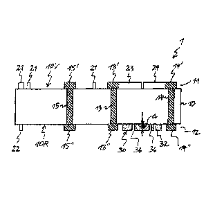
Figure 4 shows a schematic section - not true to scale
- of a multilayered film element 1 comprising a
dielectric layer 10, a first electrically conductive
layer 11 according to figure 1 arranged on the front
side 10V of the dielectric layer 10 and a second
electrically conductive layer 12 according to figure 2
arranged on the rear side 1OR of the dielectric layer
10. The section of the film element 1 runs along the
sectional line IV-IV indicated in figure 3. As
illustrated in figure 4, the first electrically
conductive layer 11 and the second electrically
conductive layer 12 are provided on the outer surface
of the dielectric layer 10. The plated-through holes 13
to 15 penetrating through the dielectric layer 10 with
the corresponding front- and rear-side contact-making
areas 13' to 15' and 13' ' to 15' ' are illustrated in a
hatched manner for better distinguishability in the
section. The thermode contact layer 30 having a layer
thickness d and having a thermode contact area 32 on
the outer end side is arranged on the rear side 1OR of
the dielectric layer 10, said thermode contact layer
having cutouts 36 running through the entire layer
thickness d.
CA 02803104 2012-12-18
29
Figure 5 shows a schematic section - not true to scale
- of the multilayered film element 1, which section
substantially corresponds to the sectional drawing
illustrated in figure 4. Figure 5 additionally
illustrates a chip 50 and two opposite thermodes 60 and
61 in a position in which they are arranged in a method
for fixing the chip 50 on the multilayered film element
1. In this case, the lower thermode 60 acts on the
rear-side thermode contact layer 30, and the upper
thermode 61, which can be embodied as a heated or
unheated pressure plunger, forms a mechanical counter-
bearing for the lower thermode 60 and acts on the chip
50. An intermediate strip (not illustrated) can be
arranged between the chip 50 and the thermode 61 and
is, for example, silicone-coated or provided with an
adhesion-reducing coating in some other way, in order
to prevent soiling or contamination of the thermode 61
with a connecting means and thus also adhesive bonding
of the thermode 61 to the chip 50. In order to simplify
the illustration, the figure does not designate all
components with their reference signs; in this regard,
reference is made to the corresponding reference signs
indicated in figure 4. The end side 32 of the thermode
contact layer 30 facing away from the dielectric layer
10 has, as the thermode contact area, the function of
serving as a contact area for a (lower) thermode 60, as
is indicated in figure 5.
Preferably, both the upper thermode 61 and the lower
thermode 60 are heated, for instance to a temperature
in the region of 200 C. The temperature of the upper
thermode 61, that is to say of the thermode on the chip
side of the film element 1, is usually higher than that
of the lower thermode 60. As a result of the
temperature spreading it is possible to obtain specific
curing effects in the case of the connecting means. A
connecting means applied between the chip 50 and the
chip contact areas 23, 24 can be thermally activated by
the heat which is emitted to the thermode contact layer
CA 02803104 2012-12-18
30 by the lower thermode 60 and is conducted through
the dielectric layer 10 to the chip contact areas 23,
24. The thermal activation of the connecting means
results in a permanent mechanical connection between
5 the chip 50 and the chip contact areas 23, 24, and thus
between the chip 50 and the multilayered film element
1. The end face of the chip 50 is smaller than the
planar end side of the upper thermode 61 and optionally
also smaller than the planar end side of the lower
10 thermode 60, in order that the thermodes 60, 61
reliably cure, around the chip 50 as well, a connecting
means that possibly emerges between the chip 50 and the
chip contact areas 23, 24.
15 A thermally activatable, e.g. thermally curable,
adhesive or a solder can be used as the connecting
means. The connecting means can be applied, before the
chip 50 is placed onto the chip contact areas 23, 24,
to that side of the chip 50 which faces the chip
20 contact areas 23, 24 and/or to that side of the chip
contact areas 23, 24 which faces the chip 50. The
thermally curable adhesive can be, for example, a
thermosetting, electrically conductive, one-component
epoxy adhesive comprising metalized, preferably
25 spherical, non-flat particles or solid metal particles,
e.g. metalized balls, flakes or platelets, which cures
in a temperature range around approximately 190 C in
approximately 8 seconds. By way of example, metal
particles composed of silver or copper which are
30 embedded into the plastics matrix are advantageous in
this context. Furthermore, however, it is also possible
to use systems whose particles are formed from graphite
and/or have other binder components which in turn form
one- or multi-component systems. By way of example,
lead, tin or palladium can be used as solder.
The dielectric layer 10 is a plastic film having a
thickness of 4 to 250 pm which serves as a carrier
substrate for the first electrically conductive layer
CA 02803104 2012-12-18
31
11 and the second electrically conductive layer 12.
Preferably, a film composed of PVC, PVC/ABS, PET,
polycarbonate, polyolefins, polypropylene, polystyrene,
polyethylene or of BOPP having a thickness of 36 to
150 pm (PET = polyethylene terephthalate; BOPP =
biaxially oriented polypropylene) is used as the
dielectric layer 10. Furthermore, it is also possible
that the dielectric layer 10 additionally comprises one
or more further layers and/or besides the dielectric
layer 10 additionally one or more further layers are
provided between the first electrically conductive
layer 11 and the second electrically conductive layer
12, and/or consists of other non-conductive materials
not mentioned above, e.g. a paper composite.
The electrically conductive layer or the first and
second electrically conductive layers 11, 12 is/are
preferably in each case a metallic layer having a
thickness of 1 pm to 50 pm, preferably of 5 to 15 pm.
The metal layer consists, for example, of iron, copper,
aluminum, nickel, silver, gold, platinum, tin, zinc or
an alloy of these metals and/or multilayer systems.
Furthermore, it is also possible that the electrically
conductive layers 11 and 12 are produced by means of at
least one electrolytic reinforcement and can thus
additionally comprise one or more conductive layers,
for example consisting of a conductive printing
material. In this context, combinations of different
techniques for producing the metallic layers are also
possible - for example electrolytic reinforcement in
combination with targeted demetallization.
The plated-through holes 13, 14 and 15 preferably
likewise consist of an electrically conductive, in
particular metallic, material introduced into
corresponding cutouts of the dielectric layer 10 and
are preferably produced by means of at least one
electrolytic process jointly with the electrically
conductive layers 11 and 12. However, it is also
CA 02803104 2012-12-18
32
possible to produce the plated-through holes by
riveting methods, crimping methods, soldering methods
and the like.
The conductor track segment 21 has - as indicated in
figure 1 - the form of a flat coil having N turns,
having a distance between the turns of 0.05 to 5 mm and
a conductor track width of 0.05 to 5 mm. The number N
of turns is preferably in the range of 2 to 10. The
outermost turn preferably encloses a rectangular area
having a width of 40 mm to 100 mm and a length of 20 mm
to 80 mm. The conductor track segment 22 preferably has
a length of more than 1/4 of the innermost turn of the
conductor track segment 21 and is shaped - as indicated
in figure 2 - preferably in the form of half to one
turn.
It is furthermore also possible for the film element 1
to have, besides the layers explained with reference to
figure 1 to figure 4, one or more further layers and to
form, for example, a laminating film, a transfer film
or a region of a transfer ply of a transfer film.
Furthermore, it is also possible for the film element 1
not to be present in separated form, but rather to be
part of a film web preferably having a multiplicity of
film elements 1 of identical type which are arranged
alongside one another.
The thermode contact layer 30 can be produced in the
same method as the electrically conductive layers 11,
12. In this case, the electrically conductive thermode
contact layer 30 can be embodied as a metallization,
for example composed of aluminum, iron, copper, nickel,
platinum, silver, gold, tin, zinc or an alloy of these
materials. Moreover, the thermode contact layer 30 in
this case can additionally fulfill a function as an
electromagnetic component. Furthermore, it is also
possible that the thermode contact layer 30 is applied
to the dielectric substrate 10 only after the formation
CA 02803104 2012-12-18
33
of the electrically conductive layers 11, 12, e.g. is
applied, e.g. adhesively bonded or fixed by means of
connecting elements, temporarily or permanently as a
finished component.
In the sections illustrated in figure 4 and figure 5,
it is evident that the cutouts 36 run through the
thermode contact layer 30 from the thermode contact
area 32 as far as the opposite end face of the thermode
contact layer 30. It is possible for an observer of the
thermode contact layer 30 to discern the dielectric
substrate 10 through the cutouts 36 in a viewing
direction perpendicular to the dielectric layer 10. By
means of coloring of the thermode contact layer 30 or
of the thermode contact area 32 and of the dielectric
layer 10 and/or shaping of the cutouts 36, an optical
information item, e.g. a pattern, a graphic, a
character such as a symbol, a letter, a number, can
thus be provided for an observer or recognition system.
It is also possible that, as a result of the emission
of heat from the thermode 60 to the thermode contact
layer 30 and the adjoining dielectric layer 10,
material of the dielectric layer melts and runs at
least partly into the cutouts 36 in the liquid state.
An improved connection of the thermode contact layer 30
and of the dielectric layer 10 can result in this way.
It is likewise possible that a layer applied to the
multilayered film element 1 in a subsequent coating
method, e.g. a surface protective layer composed of a
clearcoat or a laminating film, at least partly extends
into the cutouts 36 and/or is connected to the
dielectric layer 10 via one or more cutouts 36. An
interlayer adhesion can thereby be obtained.
Figure 6, for the purpose of better illustrating the
exemplary embodiment on the sheet of the drawings, once
again shows the first electrically conductive layer
CA 02803104 2012-12-18
34
according to figure 1 arranged on a front side of a
dielectric layer.
Figure 7 shows the second electrically conductive layer
according to figure 2 together with a further exemplary
embodiment of the thermode contact layer. As
illustrated in an enlarged manner in figure 7A, the
thermode contact layer 30 is embodied as a circular
disk having a thickness d and an external diameter Da,
which has, in a ring-shaped region having an internal
diameter Di and an external diameter Da, cutouts 36 in
the form of 90 arcs having a width b which run in each
case at a constant distance from the center axis of the
disk-shaped thermode contact layer 30. At the angular
positions at 0 , 90 , 180 and 270 , continuous webs
run from the internal diameter Di to the external
diameter Da, the arcuate cutouts 36 in each case ending
at said webs. By means of the cutouts 36 and the webs,
the thermode contact layer 30 forms, in the ring-shaped
region, concentrically extending annuli having the
width b. Typical and particularly advantageous
(identified by "preferably" in the table) values of the
layer thickness d, of the external diameter Da, of the
internal diameter Di and of the width b for the present
exemplary embodiment of the thermode contact layer 30
are indicated in column 3 of the table.
Figure 8 shows a superimposed projection of the layers
according to figure 6 and figure 7, as seen
perpendicularly to the dielectric layer. The
illustration corresponds to the illustration in figure
3, to the explanation of which reference is made.
Figure 9, for the purpose of better illustrating the
exemplary embodiment on the sheet of the drawings, once
again shows the first electrically conductive layer
according to figure 1 arranged on a front side of a
dielectric layer.
CA 02803104 2012-12-18
Figure 10 shows the second electrically conductive
layer according to figure 2 together with a further
exemplary embodiment of the thermode contact layer 30.
Figure 10A shows an enlarged excerpt from figure 10
5 with an illustration of the thermode contact layer 30.
The exemplary embodiment of the thermode contact layer
30 largely corresponds to the exemplary embodiment in
figure 7 and figure 7A, to which reference is made,
only with dimensions deviating therefrom. Typical and
10 particularly advantageous (identified by "preferably"
in the table) values of the layer thickness d, of the
external diameter Da, of the internal diameter Di and
of the width b for the present exemplary embodiment of
the thermode contact layer 30 are indicated in column 4
15 of the table.
Figure 11 shows a superimposed projection of the layers
according to figure 9 and figure 10, as seen
perpendicularly to the dielectric layer. The
20 illustration corresponds to the illustration in figure
3, to the explanation of which reference is made.
Figure 12, for the purpose of better illustrating the
exemplary embodiment on the sheet of the drawings, once
25 again shows the first electrically conductive layer
according to figure 1 arranged on a front side of a
dielectric layer.
Figure 13 shows the second electrically conductive
30 layer according to figure 2 together with a further
exemplary embodiment of the thermode contact layer 30.
Figure 13A shows an enlarged excerpt from figure 13
with an illustration of the thermode contact layer 30.
The exemplary embodiment of the thermode contact layer
35 30 largely corresponds to the exemplary embodiment in
figure 7 and figure 7A, to which reference is made,
only with dimensions deviating therefrom. Typical and
particularly advantageous (identified by "preferably"
in the table) values of the layer thickness d, of the
CA 02803104 2012-12-18
36
external diameter Da, of the internal diameter Di and
of the width b for the present exemplary embodiment of
the thermode contact layer 30 are indicated in column 5
of the table.
Figure 14 shows a superimposed projection of the layers
according to figure 12 and figure 13, as seen
perpendicularly to the dielectric layer. The
illustration corresponds to the illustration in figure
3, to the explanation of which reference is made.
Figure 15, for the purpose of better illustrating the
exemplary embodiment on the sheet of the drawings, once
again shows the first electrically conductive layer
according to figure 1 arranged on a front side of a
dielectric layer.
Figure 16 shows the second electrically conductive
layer according to figure 2 together with a further
exemplary embodiment of the thermode contact layer 30.
As illustrated in an enlarged manner in figure 16A, the
thermode contact layer 30 is embodied as a circular
disk having a thickness d and an external diameter Da,
which has, in a hollow-cylindrical region having an
internal diameter Di and an external diameter Da - 2b,
twenty-four wedge-shaped cutouts 36 arranged radially,
the tapering ends of the wedges being oriented toward
the disk axis and running parallel to the disk axis.
Typical and particularly advantageous (identified by
"preferably" in the table) values of the layer
thickness d, of the external diameter Da, of the
internal diameter Di and of the width b for the present
exemplary embodiment of the thermode contact layer 30
are indicated in column 6 of the table.
Figure 17 shows a superimposed projection of the layers
according to figure 15 and figure 16, as seen
perpendicularly to the dielectric layer. The
CA 02803104 2012-12-18
37
illustration corresponds to the illustration in figure
3, to the explanation of which reference is made.
Figure 18, for the purpose of better illustrating the
exemplary embodiment on the sheet of the drawings, once
again shows the first electrically conductive layer
according to figure 1 arranged on a front side of a
dielectric layer.
CA 02803104 2012-12-18
N
O O O I ~
N LU O (N M -i
~4 I v -i I LU N O
N N (N
O
44
O O O LU
( LU O (N M v--I (N
S-i -1 I 1-'1 I
N I- N O O
Ga
M
O O CD N N Ln O N M -I I
Ln ~4 r A (-i N v--I
1 N N (N
= r-1
44
O
I -I
C) O O N
00 a) LU O N M -A
M ~4 I c-I I v-I LU N O
N I-- N
is
.rA
1s
N
O O O to
M ~4 Ln O M r-1 N
LU -A
rI
N N N O O
N
O O O (N
N ~4 Ln O N M H LU N v--i
rI rI
N N N O
44
>1 >1 >1 >1
N a) 4) - 4)
4-I 4-4 44 u 4-I
~ ~ '~ ~ Q Q ~ Q q ~ A .Q N
~4 ~4
E-~
CA 02803104 2012-12-18
- 39 -
Figure 19 shows the second electrically conductive
layer according to figure 2 together with a further
exemplary embodiment of the thermode contact layer 30.
Figure 19A shows an enlarged excerpt from figure 19
with an illustration of the thermode contact layer 30.
The exemplary embodiment of the thermode contact layer
30 largely corresponds to the exemplary embodiment in
figure 2 and figure 2A, to which reference is made,
only with dimensions deviating therefrom. Typical and
particularly advantageous (identified by "preferably"
in the table) values of the layer thickness d, of the
external diameter Da, of the internal diameter Di and
of the width b for the present exemplary embodiment of
the thermode contact layer 30 are indicated in column 7
of the table.
Figure 20 shows a superimposed projection of the layers
according to figure 18 and figure 19, as seen
perpendicularly to the dielectric layer. The
illustration corresponds to the illustration in figure
3, to the explanation of which reference is made.
Besides the illustrated and described structuring of
the thermode contact layer, further shapings such as
e.g. linear or circular grid structures or non-
interconnected structures are conceivable, which can
arrive at equivalent results on account of a similar
degree of area occupancy.
Figures 21 to 23 show a further advantageous embodiment
of a film element according to the invention. In this
case, figure 21 shows a front side of a dielectric
layer with a conductor track 21, with front-side
contact-making areas 13', 14' of a first and a second
plated-through hole 13, 14, and with chip contact areas
23, 24 for making contact with a chip (not illustrated
here), said chip contact areas lying within the
conductor track 21. Figure 22 shows a rear side -
corresponding to figure 21 - of a dielectric layer with
CA 02803104 2012-12-18
a thermode contact layer 30 and a connecting region 25.
In this case, in this exemplary embodiment the rear
side does not comprise a further conductor track, but
rather substantially only the thermode contact layer 30
5 and the connecting region 25 between the plated-through
holes 13, 14. In this context, this is referred to as a
single-ended antenna. Figure 23 shows a superimposed
projection of the layers according to figure 21 and
figure 22, as seen perpendicularly to the dielectric
10 layer.
Figures 24 to 26 show a further advantageous embodiment
of a film element according to the invention. In this
case, figure 24 shows - similarly to figure 21 - a
156 front side of a dielectric layer with a conductor track
21, with front-side contact-making areas 13' to 15' of
plated-through holes 13 to 15 and with chip contact
areas 23 and 24 for making contact with a chip (not
illustrated here). In this case, the third plated-
20 through hole 15 is not arranged on a line with the
first 13 and the second plated-through hole 14, but
rather was positioned below them.
Figure 25 shows a rear side - corresponding to figure
25 22 - of a dielectric layer with a thermode contact
layer 30 and a connecting region 25. In this case, in
this exemplary embodiment the rear side does not
comprise a further conductor track, but rather
substantially only the thermode contact layer 30 and
30 the connecting region 25 between the plated-through
holes 14, 15. In this context, this is again referred
to as a single-ended antenna. Figure 26 shows a
superimposed projection of the layers according to
figure 24 and figure 25, as seen perpendicularly to the
35 dielectric layer.
Figures 27 to 29 show a further advantageous embodiment
of a film element according to the invention. In this
case, figure 27 shows a rear side of a dielectric layer
CA 02803104 2012-12-18
41
with a conductor track 21 and with a thermode contact
layer 30. In this case, the thermode contact layer 30
can be electrically connected (as illustrated) to the
conductor track 21 or can be arranged separately
therefrom, that is to say in a manner electrically
insulated therefrom. Figure 28 shows a front side of a
dielectric layer with chip contact areas 23 and 24 for
making contact with a chip (not illustrated here) . In
this exemplary embodiment, the front side does not have
a further conductor track and is substantially
constructed from the chip contact-making regions 23, 24
and the connecting region 25 between the plated-through
holes. Figure 29 shows a superimposed projection of the
layers according to figure 27 and figure 28, as seen
perpendicularly to the dielectric layer.
Figures 30 to 32 show a further particularly
advantageous embodiment of a film element according to
the invention. In this case, figure 30 shows a front
side of a dielectric layer - similarly to figure 24 -
with the difference that additional frontal thermode
contact layers in the form of two partial regions 30a,
30b were applied around a chip contact areas 23 and 24,
for making contact frontally with a chip (not
illustrated here). In combination with the rear-side
thermode contact layer 30, a very homogeneous
temperature distribution can be obtained with this
exemplary embodiment. Figure 32 shows in this exemplary
embodiment a superimposed projection of the layers
according to figure 30 and figure 31 as seen
perpendicularly to the dielectric layer.
It is possible that firstly a side of a chip and/or of
the chip contact areas 23, 24 which has electrical
contacts is coated with a thermally activatable
connecting means, then the side of the chip which has
the electrical contacts is arranged on the chip contact
areas 23, 24, and subsequently a frontal thermode
applies heat to or directly contacts the partial
CA 02803104 2012-12-18
42
regions 30a, 30b of the frontal thermode contact layer
and a rear-side thermode acts on, preferably contacts,
the rear-side thermode contact layer 30. The thermally
activatable connecting means is activated in this way.
After the connecting means has been activated, the
thermodes are separated, preferably lifted off, from
the frontal and rear-side thermode contact areas 30a,
30b, 30.
In this context it should be mentioned, on the one
hand, that in the case of a divided thermode contact
layer - corresponding to the embodiments according to
figure 30 - a rear-side thermode contact layer 30 can
be dispensed with since the heat transfer from the
partial regions 30a, 30b of the front-side divided
thermode contact layer to the chip contact areas 23, 24
already suffices for activating the connecting means.
Embodiments comprising a sole divided frontal or else
rear-side thermode contact layer are therefore
possible. On the other hand, it should be mentioned
that the division of the thermode contact layer is not
just restricted to the embodiment according to figure
30, but rather can have as many partial regions as
desired. However, a division into two in the manner
illustrated with a direct connection to the chip
contact areas 23 and 24 is advantageous in this case.
CA 02803104 2012-12-18
43
List of reference signs
1 Multilayered film element
Dielectric layer
1OR Rear side of 10
10V Front side of 10
11 First layer forming a first component, first
electrically conductive layer
12 Second layer forming a first component,
second electrically conductive layer
13 First plated-through hole
13', 13" Front- and rear-side contact-making areas of
13
14 Second plated-through hole
14', 14" Front- and rear-side contact-making areas of
14
Third plated-through hole
15', 15" Front- and rear-side contact-making areas of
20 Conductor track
21 First conductor track segment
22 Second conductor track segment
23 First component contact area, first chip
contact area
24 Second component contact area, second chip
contact area
Connecting region
Thermode contact layer
30a, 30b Partial region of the thermode contact layer
32 Thermode contact area
36 Cutout of 30
50 Second component, chip
60 Thermode (bottom)
61 Thermode (top, chip side)
b Line width of 30
d Layer thickness of 30
Da External diameter of 30
Di Internal diameter of 30