Note: Descriptions are shown in the official language in which they were submitted.
CA 02806086 2013-01-21
WO 2012/009768 PCT/AU2011/001101
1
ANTENNA CONFIGURATION METHOD AND APPARATUS
FIELD OF INVENTION
The present invention relates to the field of data transmission.
In one form, the invention relates to the transmission and/or reception of
data modulated signals between various devices, including loads and/or
antennas.
In another form, the invention relates to the field of transponders (tags),
such as Radio Frequency Identification Devices (RFID), interrogator
devices/systems and the transmission of data between a tag and an
interrogator.
It will be convenient to hereinafter describe the invention in relation to
transmission between a RFID tag and an interrogator, however it should be
appreciated that the present invention is not limited to that use only.
BACKGROUND ART
Throughout this specification the use of the word "inventor" in singular form
may be taken as reference to one (singular) inventor or more than one (plural)
inventor of the present invention.
One common use of tags is to adhere a tag to a certain item so the item
can be traced and/or information regarding the item can be interrogated when
needed. One such use of tags is on postal items, such as parcels, boxes and/or
envelopes. In this case, often tags with adhesive backing are adhered to an
item
such as a box. It has been observed by the inventors that a number of boxes
are
usually co-located in an area, truck or conveyor belt and thus when undergoing
interrogation of a particular tag, there are a number of items also in close
proximity of the tag being interrogated. A problem can arise when at least two
boxes are found to be close together. A tag located on one item may come into
close contact with another tag on another item. Note that in this situation
the
topsides (non adhesive sides) of the tags face each other. If this situation
occurs,
it has been observed that the tags may effectively interact and substantially
interfere or even cancel each others reply. It has been determined that when
two
tags are placed relatively close together, the resonant frequency of the
combined
tags can be close to or equal to the tag reply frequency.
For example, some tags in use generate replies at around 15.5 MHz.
Typically individual stackable tags have a resonant frequency of 25 MHz or
CA 02806086 2013-01-21
WO 2012/009768 PCT/AU2011/001101
2
higher. The resonant frequency is function of the RFID chip (stray)
capacitance,
tag antenna stray capacitance and the tag antenna inductance. As two tags are
brought close together, the resonate frequency of the combined tags reduces
below the resonant frequency of the individual tags. This reduction in the
resonant frequency is due to additional stray capacitance between the tags and
mutual inductance. It is possible, especially if the initial antenna
inductance is
relatively high enough and the tags are placed relatively close enough, that
the
resonate frequency of the 'combined' tags ends up at or near the tag reply
frequency.
In this situation, it has been observed that reply signals from one tag will
couple to the other tag. If tag reply frequency is at the resonant frequency
of the
combined tags, then this coupling will be very strong. A tag replies by
generating
a changing magnetic field. Thus, any other closely located tag will produce an
opposing magnetic field. If the coupling between the tags is relatively
strong,
then the magnetic field generated by the replying tag will be substantially
reduced
or cancelled by the other tag. Thus, the inventors have realised that in
certain
applications, tag replies can become weak and therefore difficult to receive.
One solution is to move the resonant frequency away from the tag reply
frequency. However, this is not always practical. The inventors have realised
that it is possible to reduce the coupling between the tags and thus increase
the
resonant frequency of the combined tags away from the reply frequency, for
example by lowering:
= the individual tag antenna inductance
= the individual tag antenna stray capacitance
= the mutual inductance of the combined tags, and/or
= the stray capacitance between the tags
The individual tag inductance can be lowered by either:
= using less tag antenna turns - which results in a smaller collecting
area and thus decrease the operating range of the tag
= or a larger tag with less turns
However, neither of these alternatives is considered acceptable.
WO 2012/009768 CA 02806086 2013-01-21 PCT/AU2011/001101
3
The individual tag stray capacitance can be reduced by increasing the gap
between antenna turns. This will decrease the collecting area and thus
decrease
the operating range of the tag which is also not considered acceptable.
The mutual inductance and the stray capacitance between the tags can be
reduced by keeping the tags apart; however this not practical as it is not
always
possible to control the orientation and positioning of items, especially
postal items
and thus this proposal is not considered to suit all applications.
In other applications, the item to which a tag is adhered, such as casino
chip, has a relatively shallow recess provided to accommodate the tag in a
manner some distance away from an outer edge of the casino chip. This
impedes design of tags, antennas and items to which tags are adhered.
It is to be appreciated that any discussion of documents, devices, acts or
knowledge in this specification is included to explain the context of the
present
invention. Further, the discussion throughout this specification conies about
due
to the realisation of the inventor and/or the identification of certain
related art
problems by the inventor. Moreover, any discussion of material such as
documents, devices, acts or knowledge in this specification is included to
explain
= the context of the invention in terms of the inventor's knowledge and
experience
and, accordingly, any such discussion should not be taken as an admission that
any of the material forms part of the prior art base or the common general
knowledge in the relevant art in Australia, or elsewhere, on or before the
priority
date of the disclosure and claims herein.
SUMMARY OF INVENTION
An object of the present invention is to provide an improved tag and / or
method of data transmission.
A further object of the present invention is to alleviate at least one
disadvantage associated with the related art.
It is an object of the embodiments described herein to overcome or
alleviate at least one of the above noted drawbacks of related art systems or
to at
least provide a useful alternative to related art systems.
In a first aspect of embodiments described herein there is provided a tag
comprising an antenna having a first portion having a first configuration and
a
WO 2012/009768 CA 02806086 2013-01-21 PCT/AU2011/001101
= 4
second portion having a second configuration, first configuration being
different
than the second configuration.
In another aspect of embodiments described herein there is provided a tag
comprising an antenna having a first configuration such that when placed in a
6 face to face orientation with another tag having an antenna of a second
configuration, the first configuration is not a mirror image of the second
configuration.
In yet a further aspect of embodiments described herein there is provided a
communication system comprising a first device having a first antenna, a
second
device having a second antenna, at least one of the first and second antennas
having a first portion having a first configuration and a second portion
having a
second configuration, first configuration being different than the second
configuration.
In another aspect of embodiments described herein there is provided a
method of reducing interference between a first antenna and a second antenna,
the method comprising providing the first antenna in a first shape, providing
the
second antenna in a second shape, the first shape being different to the
second
shape.
In another aspect of embodiments described herein there is provided a
method of configuring an antenna adapted to reduce mutual coupling with
another antenna, the method comprising configuring the antenna to have a
relatively non-symmetrical shape.
In another aspect of embodiments described herein there is provided a
method of configuring an antenna adapted for use with a tag, the method
comprising providing an antenna having a first configuration such that when
placed in a face to face orientation with another antenna of a second
configuration, the first configuration is not a mirror image of the second
configuration.
Other aspects and preferred forms are disclosed in the specification and/or
defined in the appended claims, forming a part of the description of the
invention.
In essence, embodiments of the present invention stem from the
realization that a relatively non-symmetrical antenna design may be used to
alleviate tag coupling. In this regard, the present invention contemplates
CA 02806086 2013-01-21
WO 2012/009768 PCT/AU2011/001101
5
providing an antenna having at least two portions, the first portion having a
first
shape and the second portion having a second shape, different from the first
shape. In one embodiment, the first portion is not a mirror image of the
second
portion different. In another embodiment, the first and second portions may
have
a substantially similar area, but each still has a different shape.
It is preferable that the lack of symmetry is relative to at least two axis.
Furthermore, providing one tag having a first antenna with a first shape,
and another tag having a second antenna with a second shape, the first and
second shaped antennas having a different shape to each other, has been
observed to alleviate undesirable tag coupling. In one form, if a
number/plurality
of tag(s) have antenna(s) that are of a different (even random) shape, then
coupling causing interference will be reduced. It has also been determined
that
even a relatively small difference in shape between one antenna and another
antenna is enough to alleviate interference between tags.
Advantages provided by the present invention comprise the following:
= Reduced coupling between proximate antennas;
= One antenna has an increased position insensitivity relative to
another antenna;
= Enables a number of tags/antennas to be used in relatively close or
confined situations/applications;
= Alleviates the need for an item to have a recess to incorporate a tag.
Throughout this specification, 'tag' is intended to include, without
limitation,
an RFID device comprising a microchip placed on a powering, transmitting
and/or
receiving antenna carried on a substrate (inlay) and that is powered
externally by
an inductive field or by a battery. It also includes a token, insert,
transponder,
chip, label, identification device, badge, inlet, inlay, ticket, wireless
memory or any
other form of identifiable device and may be rendered in any technology which
enables identification. For example, the tag may be an RFID tag. In a further
example, and without limitation, the identification device may be an ASIC,
other
microchip, an ASIC with an associated antenna assembly, or an antenna without
a chip where electronic circuitry included in the printed antenna structure,
provides the intelligence of the device, logic means or is a tuned antenna.
WO 2012/009768 CA 02806086 2013-01-21 PCT/AU2011/001101
=
6
Further scope of applicability of embodiments of the present invention will
become apparent from the detailed description given hereinafter. However, it
should be understood that the detailed description and specific examples,
while
indicating preferred embodiments of the invention, are given by way of
illustration
only, since various changes and modifications within the spirit and scope of
the
disclosure herein will become apparent to those skilled in the art from this
detailed
description.
BRIEF DESCRIPTION OF THE DRAWINGS
Further disclosure, objects, advantages and aspects of preferred and other
embodiments of the present application may be better understood by those
skilled in the relevant art by reference to the following description of
embodiments
taken in conjunction with the accompanying drawings, which are given by way of
illustration only, and thus are not limitative of the disclosure herein, and
in which:
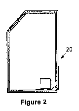
Figure 1 illustrates a prior art symmetrical tag;
Figure 2 illustrates a non symmetrical antenna design in accordance with
an embodiment of the present invention;
Figure 3 illustrates another non symmetrical antenna design in accordance
with another embodiment of the present invention;
Figure 4 illustrates shows two over lapping prior art antennas;
Figure 5 illustrates two over lapping simplified non symmetrical antennas in
accordance with an embodiment of the present invention; and
Figure 6 illustrates another two over lapping simplified alternative non
symmetrical antennas in accordance with another embodiment of the present
invention.
DETAILED DESCRIPTION
Figure 1 illustrates a prior art tag 10. The antenna 11 has a relatively
symmetrical shape, at least a symmetry about one axis. When a prior art tag 10
as shown in Figure 1 is placed in a face to face relationship with another,
similar,
tag the positioning of the tags will be as represented in Fig.4. In figure 4,
although each tag antenna 40 and 41(as represented by dotted and solid lines
respectively) is made up of a number of turns, for the sake of ease of
understanding of the present invention, these turns are represented in Figure
4 by
a single line (solid or dotted). Also, for clarity the antennas 40 and 41 have
been
CA 02806086 2013-01-21
WO 2012/009768 PCT/AU2011/001101
7
drawn slightly misaligned, so the shape of each antenna can be discerned. It
can
be seen that the antenna of one tag 40 is aligned with antenna 41 of another
tag,
when the two antennas are placed face to face with each other. Tags that use
symmetrical antenna designs can be aligned so one tag antenna sits directly or
closely on top of the next tag antenna. This means that the antenna turns for
the
two tags overlap and are thus very close to each other. In operation, this
results
in a high mutual inductance and high stray capacitance between the antennas 40
and 41, and thus interference.
Figures 2 and 3 show examples of antenna designs 20 and 30 according
to the present invention. The antennas are shaped so that, when placed face to
face with a corresponding antenna of a similar shape, there is reduced
interference. This is illustrated in Figures 5 and 6.
Figure 5 shows two over lapping simplified non symmetrical antennas 50
and 51. These antennas 50 and 51 are illustrated face to face (topside to
topside
or bottom side to bottom side). Again these antennas have been draw slightly
misaligned for the sake of clarity. Unlike the symmetrical antennas
illustrated in
Figures 1 and 4, the antennas according to the present invention, when placed
face to face, do not substantially align with each other. That is, at least
one area
52 is provided in which the antennas do not overlap. This results in a reduced
mutual inductance and stray capacitance between the antennas. In other words,
the antenna shape according to the present invention is configured in such a
way
that two antennas 51 and 51 cannot be positioned so that the antennas turns
substantially cover or align with each other. It may be said that the antenna
configuration of the present invention provides an asymmetric antenna shape.
Figure 6 shows another example of two over lapping simplified alternative
non symmetrical antennas 60 and 61. Again the antennas are illustrated in a
face
to face alignment. Again, the antennas are shaped so that a region 62 is
provided in which the antennas do not overlap.
In applications where tags according to the present invention are stuck on
to items including boxes, the boxes can be stored such that the tags are
perfectly
or closely aligned and touch or almost touch, face to face, topside to topside
or
bottom side to bottom side. In this position, it has been found that, whereas
in the
prior art, there is relatively strong coupling between the tags and thus the
CA 02806086 2013-01-21
WO 2012/009768 PCT/AU2011/001101
8
possibility of weak replies, in the present invention, with the use of tags
having
antennas of a different shape and/or a non symmetrical antenna design, the
coupling between the tags will be reduced.
The solution to this problem, which we want to patent, is to use a non-.
symmetrical tag antenna design. In this application tags are stuck on to items
including boxes. The boxes can be stored such that the tags are perfectly or
closely aligned and touch or almost touch, topside to topside. In this
position
there is strong coupling between the tags and thus the possibility of weak
replies.
If a non symmetrical antenna design Is used the coupling between the tags will
be
reduced.
The present invention is applicable, at least, to RFID antenna(s).
While this invention has been described in connection with specific
embodiments thereof, it will be understood that it is capable of further
modification(s). This application is intended to cover any variations uses or
adaptations of the invention following in general, the principles of the
invention
and including such departures from the present disclosure as come within known
or customary practice within the art to which the invention pertains and as
may be
applied to the essential features hereinbefore set forth.
As the present invention may be embodied in several forms without
departing from the spirit of the essential characteristics of the invention,
it should
be understood that the above described embodiments are not to limit the
present
invention unless otherwise specified, but rather should be construed broadly
within the spirit and scope of the invention as defined in the appended
claims.
The described embodiments are to be considered in all respects as illustrative
only and not restrictive.
Various modifications and equivalent arrangements are intended to be
included within the spirit and scope of the invention and appended claims.
Therefore, the specific embodiments are to be understood to be illustrative of
the
many ways in which the principles of the present invention may be practiced.
In
the following claims, means-plus-function clauses are intended to cover
structures
as performing the defined function and not only structural equivalents, but
also
equivalent structures. For example, although a nail and a screw may not be
structural equivalents in that a nail employs a cylindrical surface to secure
WO 2012/009768 CA 02806086 2013-01-21PCT/AU2011/001101
9
wooden parts together, whereas a screw employs a helical surface to secure
wooden parts together, in the environment of fastening wooden parts, a nail
and a
screw are equivalent structures.
"Comprises/comprising" and "includes/including" when used in this
specification is taken to specify the presence of stated features, integers,
steps or
components but does not preclude the presence or addition of one or more other
features, integers, steps, components or groups thereof. Thus, unless the
context clearly requires otherwise, throughout the description and the claims,
the
words 'comprise', 'comprising', 'includes', 'including' and the like are to be
construed in an inclusive sense as opposed to an exclusive or exhaustive
sense;
that is to say, in the sense of Including, but not limited to".