Note: Descriptions are shown in the official language in which they were submitted.
- 1 -
Medical Device
BACKGROUND
The present invention relates to the field of medical devices and in
particular, although
not exclusively, to medical cauterization and cutting devices. The invention
also relates
to drive circuits and methods for driving such medical devices.
Many surgical procedures require cutting or ligating blood vessels or other
internal tissue.
Many surgical procedures are performed using minimally invasive techniques, a
hand-
held cauterization device is used by the surgeon to perform the cutting or
ligating. The
existing hand-held cauterization devices require a desk top power supply and
control
electronics that are connected to the device through an electrical supply
line. Figure 10
illustrates such an existing hand-held cauterization device currently in use.
It has been known for a number of years that these existing devices are
cumbersome
and difficult to use during a surgical operation due to the large size of the
supply and
control electronics and due to the tethering of the hand-held cauterization
device to the
supply and control electronics. It has also been known for a number of years
that these
problems would be overcome by providing a battery powered hand-held
cauterization
device in which the power and control electronics are mounted within the
device itself,
such as within the handle of the device. However, it is not a simple matter of
miniaturising the electronics. The power that has to be supplied to the device
during the
surgical procedure and the current design of the electronics is such that
large capacitors,
inductors and transformers as well as heat sinks and fans are required. Figure
11
illustrates in more detail the different parts of the supply and control
electronics that are
used in the existing design as illustrated in Figure 10. Whilst it is possible
to reduce the
size of the sensing and control electronics, other parts of the circuitry
cannot be
miniaturised in this way.
In particular, the existing electronics design uses circuitry for providing an
adjustable 24
Volt power supply; FETs and associated drive circuitry; a transformer for
increasing the
CAN_DMS: \108786260\1
CA 2806164 2017-09-22
- 2 -
supply voltage; and filtering circuitry to remove harmonics from the square
wave voltage
levels that are generated by the FET switches and the transformer. Given the
voltage
levels and the power levels used to drive the cauterization device, the
transformers and
output filters all have to be relatively bulky devices and large heat sinks
and a fan are
required to cool the FET switches.
SUMMARY
The present invention aims to provide an alterative circuit design that will
allow the
miniaturisation of the circuitry so that it can be built into the hand-held
cauterization
device, whilst still being able to provide the power and control required for
the medical
procedure.
The present invention provides a medical device comprising an end effector
having at least
one electrical contact a radio frequency, RF, generation circuit for
generating an RF drive
signal and to provide the RF drive signal to the at least one electrical
contact and wherein
the RF generation circuit comprises a resonant circuit. In one embodiment, the
radio
frequency generation circuit comprises switching circuitry that generates a
cyclically varying
signal, such as a square wave signal, from a DC supply and the resonant
circuit is
configured to receive the cyclically varying signal from the switching
circuitry. The DC supply
is preferably provided by one or more batteries that can be mounted in a
housing (such as a
handle) of the device.
According to another aspect, the invention provides a medical device
comprising. a handle
for gripping by a user; an end effector coupled to the handle, the end
effector having at least
one electrical contact; battery terminals for connecting to one or more
batteries; a radio
frequency, RF, generation circuit coupled to said battery terminals and
operable to generate
an RF drive signal and to provide the RF drive signal to the at least one
electrical contact of
said end effector; wherein the frequency generation circuit comprises:
switching circuitry for
generating a cyclically varying signal (which may be a square wave pulse width
modulated
signal) from a potential difference across said battery terminals; and a
resonant drive circuit
coupled to said switching circuitry and operable to filter the cyclically
varying signal
CAN_DMS. \108786260\1
CA 2806164 2017-09-22
- 3 -
generated by the switching circuitry; and wherein the RF drive signal is
obtained using an
output signal from said resonant circuit.
The medical device may also comprise a control circuit (which may comprise
hardware
and/or software) that varies the frequency of the RF drive signal. The control
circuit may
vary the frequency based on a measurement of the RF drive signal in order to
control at
least one of the power, voltage and/or current delivered to the at least one
electrical contact
of the end effector. In a preferred embodiment, the measurement is obtained
from a
sampling circuit that operates synchronously with respect to the frequency of
the RF drive
signal. The frequency at which the sampling circuit samples the sensed signal
may be an
integer fraction of the frequency of the RF drive signal.
In one embodiment, the control circuit varies the frequency of the RF drive
signal around
(preferably just above or just below) the resonant frequency of the resonant
circuit. The
resonant characteristic of the resonant circuit may vary with a load connected
to the at least
one electrical contact and the control circuit may be arranged to vary the RF
drive frequency
to track changes in the resonant characteristic of the resonant circuit.
According to another aspect, the invention provides a medical device
comprising: a handle
for gripping by a user; an end effector coupled to the handle and having at
least one
electrical contact; a radio frequency, RF, generation circuit operable to
generate an RF drive
signal and to provide the RF drive signal to the at least one electrical
contact; and a control
circuit operable to vary the frequency of the RF drive signal to control at
least one of the
power, the voltage and the current provided to the at least one contact of the
end effector.
The RF generation circuit may comprise a signal generator that generates a
cyclically
varying signal at the RF frequency; and a frequency dependent attenuator that
attenuates
the cyclically varying signal in dependence upon the frequency of the
cyclically varying
signal. The frequency dependent attenuator may be a lossless attenuator and
may
comprise a resonant circuit having a resonant frequency at or near the RF
frequency of the
cyclically varying signal.
CAN_DMS: \108786260\1
CA 2806164 2017-09-22
- 4 -
The present invention also provides a medical device comprising: a handle for
gripping by a
user; an end effector coupled to the handle and having at least one electrical
contact; a radio
frequency, RF, generation circuit operable to generate an RF drive signal and
to provide the
RF drive signal to the at least one electrical contact; an input for receiving
a sensed signal
that varies with the RF drive signal applied to the at least one electrical
contact; a sampling
circuit for sampling the sensed signal received at said input; a measurement
circuit operable
to make measurements of the RF drive signal using samples obtained from the
sampling
circuit; and a control circuit operable to control the RF generation circuit
in dependence upon
the measurements made by the measurement circuit, to vary the frequency of the
generated
RF drive signal; wherein the sampling circuit is operable to sample the sensed
signal at a
sampling frequency that varies in synchronism with the frequency of the RF
drive signal.
The invention also provides a method of operating a medical device comprising
generating
an RF signal and applying the RF signal to at least one electrode of an end
effector of the
medical device and controlling the frequency of the generated RF signal to
control at least
one of the power, current, and voltage applied to the at least one electrode.
According to another aspect, the invention provides a method of cauterising a
vessel or
tissue, the method comprising: gripping the vessel or tissue with an end
effector of a medical
device; applying an RF signal to at least one electrode of the end effector
that is in contact
with the vessel or tissue; and controlling the frequency of the RF signal to
control at least
one of the power, current, and voltage applied to the tissue to perform the
cauterisation.
The above methods may use the above described medical device, although that is
not
essential.
The controlling step may vary the frequency of the RF signal to control the
power applied to
the tissue or vessel, and the method may further comprise obtaining
measurements of the
impedance of the tissue or vessel and varying the desired power applied to the
tissue or
vessel in dependence upon the obtained impedance measurements.
In one aspect, a medical device comprises: a handle for gripping by a user; an
end effector
coupled to the handle and having at least one electrical contact; a radio
frequency (RF)
CAN_DMS. \108786260\1
CA 2806164 2017-09-22
- 5 -
generation circuit coupled to the handle and operable to generate an RF drive
signal and to
provide the RF drive signal to the at least one electrical contact, wherein
the RF generation
circuit comprises a resonant circuit; and a control circuit comprising a
sampling circuit,
wherein the control circuit is configured to vary a frequency of the RF drive
signal around a
resonant frequency of the resonant circuit and configured to determine the
frequency and a
phase of the RF drive signal and generate a sampling frequency, and wherein
the sampling
circuit is configured to sample a sensed voltage signal or a sensed current
signal at the
sampling frequency, such that the sampling frequency is synchronized with the
frequency
and the phase of the RF drive signal.
In one aspect, a medical device comprises: a handle for gripping by a user; an
end
effector coupled to the handle and having at least one electrical contact; a
radio
frequency (RF) generation circuit operable to generate an RF drive signal and
to provide
the RF drive signal to the at least one electrical contact; a
frequency dependent
attenuator comprising a resonant circuit; and a control circuit comprising a
sampling
circuit, wherein the control circuit is operable to vary a frequency of the RF
drive signal
around a resonant frequency of the resonant circuit to control at least one of
a power, a
voltage or a current provided to the at least one contact of the end effector
and is
configured to determine the frequency and a phase of the RF drive signal and
generate a
sampling frequency, and wherein the sampling circuit is configured to sample a
sensed
voltage signal or a sensed current signal at the sampling frequency, such that
the
sampling frequency is synchronized with the frequency and the phase of the RF
drive
signal.
FIGURES
These and various other features and aspects of the invention will become
apparent from
the following detailed description of embodiments which are described with
reference to
the accompanying Figures in which:
Figure 1 illustrates a hand-held cauterization device that has batteries and
drive and
control circuitry mounted into a handle portion of the device;
CAN_DMS: \108786260\1
CA 2806164 2017-09-22
- 5a -
Figure 2 is a part block part schematic diagram illustrating the main
components of the
RF drive circuitry and control circuitry used in one embodiment of the
invention;
Figure 3 is a block diagram illustrating the main components of a controller
used to
control the operation of the RF drive circuitry illustrated in Figure 2;
Figure 4 is a timing diagram illustrating the RF drive signals applied to the
cauterization
device and illustrating a way in which synchronous samples may be obtained to
measure
the drive signals;
Figure 5a is a plot illustrating limits that are placed on voltage and current
supplied to the
cauterization device illustrated in Figure 1;
Figure 5b illustrates a resulting power plot obtained by combining the current
and voltage
plots illustrated in Figure 5a;
Figure 6 is a plot illustrating the way in which the resonant characteristics
of the RF drive
circuit illustrated in Figure 2 varies with different loads;
Figure 7 is a flow chart illustrating the operation of a frequency control
algorithm used to
control the frequency of the RF drive signals applied to the cauterization
device;
Figure 8 is a plot illustrating one way in which the power limit can be varied
by the control
electronics during a surgical procedure;
Figure 9 is a part block part schematic diagram illustrating the main
components of
another RF drive circuit and control circuit embodying the invention;
Figure 10 illustrates the form of a prior art hand-held cauterization device
which is
connected to power supply and control electronics via a power supply line; and
Figure 11 is a plan view illustrating the different components of the existing
electronics
used to drive and control the hand-held cauterization device illustrated in
Figure 10.
CAN_DMS: \108786260\1
CA 2806164 2017-09-22
- 5b -
DETAILED DESCRIPTION
Medical Device
CAN_DMS: \108786260\1
CA 2806164 2017-09-22
CA 02806164 2013-01-21
WO 2011/144911 PCT/GB2011/000778
- 6 -
Many surgical procedures require cutting or ligating blood vessels or other
vascular
tissue. With minimally invasive surgery, surgeons perform surgical operations
through a
small incision in the patient's body. As a result of the limited space,
surgeons often have
difficulty controlling bleeding by clamping and/or tying-off transected blood
vessels. By
utilizing electrosurgical forceps, a surgeon can cauterize,
coagulate/desiccate, and/or
simply reduce or slow bleeding by controlling the electrosurgical energy
applied through
jaw members of the electrosurgical forceps.
Figure 1 illustrates the form of an electrosurgical medical device 1 that is
designed
for minimally invasive medical procedures, according to one embodiment of the
present invention. As shown, the device 1 is a self contained device, having
an
elongate shaft 3 that has a handle 5 connected to the proximal end of the
shaft 3
and an end effector 7 connected to the distal end of the shaft 3. In this
embodiment,
the end effector 7 comprises medical forceps 9 and a cutting blade (not shown)
that
are controlled by the user manipulating control levers 11 and 13 of the handle
5.
During a surgical procedure, the shaft 3 is inserted through a trocar to gain
access to the
patient's interior and the operating site. The surgeon will manipulate the
forceps 9 using
the handle 5 and the control levers 11 and 13 until the forceps 9 are located
around the
vessel to be cauterised. Electrical energy at an RF frequency (it has been
found that
frequencies above about 50kHz do not affect the human nervous system) is then
applied, in a controlled manner, to the forceps 9 to perform the desired
cauterisation. As
shown in Figure 1, in this embodiment, the handle 5 houses batteries 15 and
control
electronics 17 for generating and controlling the electrical energy required
to perform the
cauterisation. In this way, the device 1 is self contained in the sense that
it does not
need a separate control box and supply wire to provide the electrical energy
to the
forceps 9.
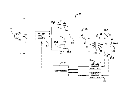
RF Drive Circuitry
Figure 2 is a part schematic part block diagram illustrating the RF drive and
control
circuitry 20 used in this embodiment to generate and control the RF electrical
energy
supplied to the forceps 9. As will be explained in more detail below, in this
embodiment,
CA 02806164 2013-01-21
WO 2011/144911 PCT/GB2011/000778
- 7 -
the drive circuitry 20 is a resonant based circuit and the control circuitry
operates to
control the operating frequency of the drive signal so that it is varied
around the resonant
frequency of the drive circuit, which in turn controls the amount of power
supplied to the
forceps 9. The way that this is achieved will become apparent from the
following
description.
As shown in Figure 2, the drive circuitry 20 comprises the above described
batteries 15
that are arranged to supply, in this example, OV and 24V rails. An input
capacitor (Cm)
21 is connected between the OV and the 24V rails for providing a low source
impedance.
A pair of FET switches 23-1 and 23-2 (both of which are N-channel in this
embodiment
to reduce power losses) is connected in series between the OV rail and the 24V
rail. FET
gate drive circuitry 25 is provided that generates two drive signals ¨ one for
driving each
of the two FETs 23. The FET gate drive circuitry 25 generates drive signals
that causes
the upper FET (23-1) to be on when the lower FET (23-2) is off and vice versa.
This
causes the node 27 to be alternately connected to the 24V rail (when FET 23-1
is
switched on) and the OV rail (when the FET 23-2 is switched on). Figure 2 also
shows
the internal parasitic diodes 28-1 and 28-2 of the corresponding FETs 23,
which conduct
during any periods that the FETs 23 are open.
As shown in Figure 2, the node 27 is connected to a capacitor-inductor-
inductor resonant
circuit 28 formed by capacitor Cs 29, inductor Ls 31 and inductor Lm 33. The
FET gate
driving circuitry 25 is arranged to generate drive signals at a drive
frequency (fd) that
opens and closes the FET switches 23 at around the resonant frequency of the
resonant
circuit 28. As a result of the resonant characteristic of the resonant circuit
28, the square
wave voltage at node 27 will cause a substantially sinusoidal current at the
drive
frequency (fd) to flow within the resonant circuit 28. As illustrated in
Figure 2, the inductor
Lm 33 is the primary of a transformer 35, the secondary of which is formed by
inductor
I-sec 37- The transformer 35 up-converts the drive voltage (Vd) across
inductor L., 33 to
the load voltage (V1) that is applied to the load (represented by the load
resistance Road
39 in Figure 2) corresponding to the impedance of the forceps' jaws and any
tissue or
vessel gripped by the forceps 9. As shown in Figure 2, a pair of DC blocking
capacitors
Ct440-1 and 40-2 is provided to prevent any DC signal being applied to the
load 39.
CA 02806164 2013-01-21
WO 2011/144911 PCT/GB2011/000778
eh
=0 -
In this embodiment, the amount of electrical power supplied to the forceps 9
is controlled
by varying the frequency of the switching signals used to switch the FETs 23.
This works
because the resonant circuit 28 acts as a frequency dependent (lossless)
attenuator.
The closer the drive signal is to the resonant frequency of the resonant
circuit 28, the
less the drive signal is attenuated. Similarly, as the frequency of the drive
signal is
moved away from the resonant frequency of the circuit 28, the more the drive
signal is
attenuated and so the power supplied to the load reduces. In this embodiment,
the
frequency of the switching signals generated by the FET gate drive circuitry
25 is
controlled by a controller 41 based on a desired power to be delivered to the
load 39 and
measurements of the load voltage (VI) and of the load current (it) obtained by
conventional voltage sensing circuitry 43 and current sensing circuitry 45.
The way that
the controller 41 operates will be described in more detail below.
Controller
Figure 3 is a block diagram illustrating the main components of the controller
41. In this
embodiment, the controller 41 is a micro-processor based controller and so
most of the
components illustrated in Figure 3 are software based components. However, a
hardware based controller 41 may be used instead. As shown, the controller 41
includes
synchronous 1,0 sampling circuitry 51 that receives the sensed voltage and
current
signals from the sensing circuitry 43 and 45 and obtains corresponding samples
which
are passed to a power, Vnes and Ines calculation module 53. The calculation
module 53
uses the received samples to calculate the RMS voltage and RMS current applied
to the
load 39 (forceps 9 and tissue/vessel gripped thereby) and from them the power
that is
presently being supplied to the load 39. The determined values are then passed
to a
frequency control module 55 and a medical device control module 57. The
medical
device control module 57 uses the values to determine the present impedance of
the
load 39 and based on this determined impedance and a pre-defined algorithm,
determines what set point power (Pset) should be applied to the frequency
control module
55. The medical device control module 57 is in turn controlled by signals
received from a
user input module 59 that receives inputs from the user (for example pressing
buttons or
activating the control levers 11 or 13 on the handle 5) and also controls
output devices
CA 02806164 2013-01-21
WO 2011/144911 PCT/GB2011/000778
- 9 -
(lights, a display, speaker or the like) on the handle 5 via a user output
module 61.
The frequency control module 55 uses the values obtained from the calculation
module
53 and the power set point (Pset) obtained from the medical device control
module 57 and
predefined system limits (to be explained below), to determine whether or not
to increase
or decrease the applied frequency. The result of this decision is then passed
to a square
wave generation module 63 which, in this embodiment, increments or decrements
the
frequency of a square wave signal that it generates by 1kHz, depending on the
received
decision. As those skilled in the art will appreciate, in an alternative
embodiment, the
frequency control module 55 may determine not only whether to increase or
decrease
the frequency, but also the amount of frequency change required. In this case,
the
square wave generation module 63 would generate the corresponding square wave
signal with the desired frequency shift. In this embodiment, the square wave
signal
generated by the square wave generation module 63 is output to the FET gate
drive
circuitry 25, which amplifies the signal and then applies it to the FET 23-1.
The FET gate
drive circuitry 25 also inverts the signal applied to the FET 23-1 and applies
the inverted
signal to the FET 23-2.
Drive Signals and Signal Measurements
Figure 4 is a signal plot illustrating the switching signals applied to the
FETs 23; a
sinusoidal signal representing the measured current or voltage applied to the
load 39;
and the timings when the synchronous sampling circuitry 51 samples the sensed
load
voltage and load current. In particular, Figure 4 shows the switching signal
(labelled
PWM1H) applied to upper FET 23-1 and the switching signal (labelled PWM1L)
applied
to lower FET 23-2. Although not illustrated for simplicity, there is a dead
time between
PWM1H and PWM1L to ensure that that both FETs 23 are not on at the same time.
Figure 4 also shows the measured load voltage/current (labelled OUTPUT). Both
the
load voltage and the load current will be a sinusoidal waveform, although they
may be
out of phase, depending on the impedance of the load 39. As shown, the load
current
and load voltage are at the same drive frequency (Id) as the switching signals
(PWM1H
and PWM1L) used to switch the FETs 23. Normally, when sampling a sinusoidal
signal,
it is necessary to sample the signal at a rate corresponding to at least twice
the
CA 02806164 2013-01-21
WO 2011/144911 PCT/GB2011/000778
- -
frequency of the signal being sampled ¨ i.e. two samples per period. However,
as the
controller 41 knows the frequency of the switching signals, the synchronous
sampling
circuit 51 can sample the measured voltage/current signal at a lower rate. In
this
embodiment, the synchronous sampling circuit 51 samples the measured signal
once per
period, but at different phases in adjacent periods. In Figure 4, this is
illustrated by the "I"
sample and the "Q" sample. The timing that the synchronous sampling circuit 51
makes
these samples is controlled, in this embodiment, by the two control signals
PWM2 and
PWM3, which have a fixed phase relative to the switching signals (PWM1H and
PWM1L)
and are out of phase with each other (preferably by quarter of the period as
this makes
the subsequent calculations easier). As shown, the synchronous sampling
circuit 51
obtains an "I" sample on every other rising edge of the PWM2 signal and the
synchronous sampling circuit 51 obtains a "Q" sample on every other rising
edge of the
PWM3 signal. The synchronous sampling circuit 51 generates the PWM2 and PWM3
control signals from the square wave signal output by the square wave
generator 63
(which is at the same frequency as the switching signals PWM1H and PWM1L).
Thus
when the frequency of the switching signals is changed, the frequency of the
sampling
control signals PWM2 and PWM3 also changes (whilst their relative phases stay
the
same). In this way, the sampling circuitry 51 continuously changes the timing
at which it-
samples the sensed voltage and current signals as the frequency of the drive
signal is
changed so that the samples are always taken at the same time points within
the period
of the drive signal. Therefore, the sampling circuit 51 is performing a
"synchronous"
sampling operation Instead of a more conventional sampling operation that just
samples
the input signal at a fixed sampling rate defined by a fixed sampling clock.
The samples obtained by the synchronous sampling circuitry 51 are then passed
to the
power, \inns and Inns calculation module 53 which can determine the magnitude
and
phase of the measured signal from just one "I" sample and one "Q" sample of
the load
current and load voltage. However, in this embodiment, to achieve some
averaging, the
calculation module 53 averages consecutive "I" samples to provide an average
"I" value
and consecutive "0" samples to provide an average "Q" value; and then uses the
average I and 0 values to determine the magnitude and phase of the measured
signal
(in a conventional manner). As those skilled in the art will appreciate, with
a drive
CA 02806164 2013-01-21
WO 2011/144911 PCT/GB2011/000778
- -
frequency of about 400kHz and sampling once per period means that the
synchronous
sampling circuit 51 will have a sampling rate of 400kHz and the calculation
module 53
will produce a voltage measure and a current measure every 0.01ms. The
operation of
the synchronous sampling circuit 51 offers an improvement over existing
products, where
measurements can not be made at the same rate and where only magnitude
information
is available (the phase information being lost).
Limits
As with any system, there are certain limits that can be placed on the power,
current and
voltage that can be delivered to the forceps 9. The limits used in this
embodiment and
how they are controlled will now be described.
In this embodiment, the RF drive circuitry 20 is designed to deliver a power
limited sine wave
into tissue with the following requirements:
1) Supplied with a nominally 24V DC supply
2) Substantially sinusoidal output waveform at approximately 400kHz
3) Power limited output of 45W
4) Current limited to 1.4Aõns and voltage limited to 85V,,,
The last two requirements are represented graphically in Figures 5a and 5b. In
particular,
Figure 5a illustrates idealised plots of voltage and current for loads between
1 Ohm and 10k
Ohms on a logarithmic scale; and Figure 5b illustrates the power delivered to
the load 39 for
loads between 1 Ohm and 10k Ohms.
The frequency control module 55 maintains data defining these limits and uses
them to
control the decision about whether to increase or decrease the excitation
frequency.
Resonant Characteristic and Frequency Control
As mentioned above, the amount of electrical power supplied to the forceps 9
is controlled
by varying the frequency of the switching signals used to switch the FETs 23.
This is
achieved by utilising the fact that the impedance of the resonant circuit 28
changes rapidly
with frequency. Therefore by changing the frequency of the switching signals,
the magnitude
CA 02806164 2013-01-21
WO 2011/144911 PCT/GB2011/000778
- 12 -
of the current through the resonant circuit 28, and hence through the load 39,
can be varied
as required to regulate the output power.
As those skilled in the art will appreciate, the resonant circuit 28 is
coupled to a load 39
whose impedance will vary during the surgical procedure. Indeed the medical
device control
module 57 uses this variation to determine whether the tissue or vessel has
been cauterised,
coagulated/desiccated. The varying impedance of the load 39 changes the
frequency
characteristic of the RF drive circuit 20 and hence the current that flows
through the resonant
circuit 28. This is illustrated in Figure 6, which is a plot 65 illustrating
the way in which the
current through the resonant circuit 28 varies with the drive frequency for a
fixed value of
load impedance. As the impedance of the load 39 increases, the resonant
characteristic 65
will change shape (the peak may grow or reduce in height) and will move to the
left and as
the impedance of the load decreases it will change its shape and move to the
right.
Therefore, the frequency control module 55 must operate quickly enough to
track the
changes in the resonant characteristic 65. This is easily achievable in this
embodiment,
where power, current and voltage measurements are available every 0.01ms. In
general
terms, measurements would only be required at a rate of about once every 0.1s
to track the
changes. However sudden changes in the resonant characteristic 65 can occur,
which the
frequency control module 55 cannot track. When this happens, the frequency
control
module 55 resets the operating frequency to a value where it knows that it
will be on one
side of the characteristic.
As the impedance of the resonant circuit 28 increases sharply both above and
below
resonance, it is possible to operate the RF drive circuit 20 either above or
below the
resonant frequency. In this embodiment, the frequency control module 55
controls the
operation of the drive circuit 20 so that it operates slightly above the
resonant frequency as
this should lead to lower switching losses through the FETs 23.
Figure 7 illustrates the processing performed In this embodiment by the
calculation module
53 and the frequency control module 55. As shown, at the beginning of the
process in step
81, the control module 55 turns on the RF drive signal at the system defined
maximum
frequency by passing an initialisation signal to the square wave generation
module 63.
Provided the control module 55 has not received, in step s3, a power down
signal from the
CA 02806164 2013-01-21
WO 2011/144911 PCT/GB2011/000778
- 1:3 -
medical device control module 57, the processing proceeds to step s5 where the
calculation
module 53 obtains the voltage and current samples from the synchronous
sampling circuitry
51. In step Si the calculation module 53 calculates the square of the voltage
and the square
of the current and the delivered power by multiplying the measured voltage by
the measured
current. These calculated values are then passed to the frequency control
module 55 which
compares, in step s9, the values with the defined limits for the applied
voltage, current and
power. The voltage and current limits are static limits that are defined in
advance. However,
the power limit depends on the medical procedure and is defined by the power
set point
(Pset) provided by the medical device control module 57. If each of the
measured values is
below the corresponding limit then, in step $11, the frequency control module
55 decides to
decrease the drive frequency and a decrease command is passed to the square
wave
generator 63. At the start of the processing, the drive frequency is set to a
defined
maximum value (in this embodiment 500kHz), which will always be above the
resonant peak
of the characteristic 65, regardless of the load impedance. Therefore,
regardless of the load
39, the initial operating frequency should be on the right hand side of the
resonant plot
shown in Figure 6. By decreasing the drive frequency, the drive frequency will
get closer to
the resonant frequency of the resonant circuit 28. As a result, the applied
current will
increase and more power will be delivered to the load 39. The processing then
returns to
step s3 and the above process is repeated.
Therefore, the current and power applied to the load 39 should increase until
one of the
limits is reached. At this point, the control module 55 will determine, in
step s9, that a limit
has been reached and so will proceed to step s13, where the control module 55
decides to
increase the drive frequency and sends the square wave generation module 63 an
increase
command. This will cause the drive frequency to move away from the resonant
frequency of
the circuit 28 and so the current and power delivered to the load 39 will
reduce. The
processing will then return to step s3 as before.
Thus, by starting on one side of the resonant peak and slowly moving the drive
frequency
towards and away from the resonant peak, the current and power level applied
to the load 39
can be controlled within the defined limits even as the impedance of the load
changes and
the resonant characteristic 65 of the resonant circuit 28 changes as the
tissue/vessel is
cauterised.
=
CA 02806164 2013-01-21
WO 2011/144911 PCT/GB2011/000778
As those skilled in the art will appreciate, it would also be possible to
start on the left hand
side of the resonant peak and increase the drive frequency to increase the
delivered power
and decrease the drive frequency to decrease the delivered power.
Medical Device Control Module
As mentioned above, the medical device control module 57 controls the general
operation of
the cauterisation device 1. It receives user inputs via the user input module
59. These
inputs may specify that the jaws of the forceps 9 are now gripping a vessel or
tissue and that
the user wishes to begin cauterisation. In response, in this embodiment, the
medical device
control module 57 initiates a cauterisation control procedure. Initially, the
medical device
control module 67 sends an initiation signal to the frequency control module
55 and obtains
current and power measurements from the calculation module 53. The medical
device
control module 57 then checks the obtained values to make sure that the load
39 is not open
circuit or short circuit. If it is not, then the medical device control module
57 starts to vary the
power set point to perform the desired cauterisation. Figure 8 is a plot
illustrating the way in
which the medical device control module 57 may vary the set point power to
achieve the
desired cauterisation procedure. Various other techniques and other power
delivery
algorithms may also be used.
As shown in Figure 8, during an initial period 71 the medical device control
module 57 pulses
the set point power between zero and about 10 Watts. Then during a main
cauterisation
period 73 (which typically lasts for about 5 seconds) the medical device
control module 57
pulses the set point power between zero and 50 Watts. During this period, the
medical
control device receives the power and voltage measurements from the
calculation module 53
and calculates from them the impedance of the load 39. The medical device
control module
57 determines that the cauterisation is complete when the calculated impedance
exceeds a
threshold. Finally, the medical device control module 57 performs a
terminating procedure
during a terminating period 75. During the terminating procedure, the medical
device control
module 57 varies the set point power and checks that cauterisation has been
achieved (by
checking the impedance of the load using the measured power and current
values) and re-
enters the main cauterisation period again if it determines that cauterisation
has not been
completed.
CA 02806164 2013-01-21
WO 2011/144911 PCT/GB2011/000778
- lb -
Resonant Circuit Design
The way that the values of the inductors and capacitors were chosen in this
embodiment will
now be described. As those skilled in the art will appreciate, other design
methodologies
may be used.
The complex impedance of the circuit shown in Figure 2 can be approximated by
the
following equation:
1 j2;rflõõRioad
Z = j2refL., + _____________ +R (1)
j2ffir8 pirfLõõ+ Rioad_sef
Where:
Figuacref is the load resistance referred to the primary (by the square of the
turns ratio);
R, represents the equivalent series resistance of the inductor, transformer
capacitor and
switching devices..
All other component non-idealities are ignored and the transformer is
considered to be ideal
as a first approximation.
Assuming that R, is small, when the load is open circuit (le Rload_mi is
infinite) the resonant
frequency can be shown to be:
1
(2)
27r4(L, + LOC.,
Similarly, when the load is short circuit (ie Rioad_rof is zero) the resonant
frequency can be
shown to be:
1
= 21c1. (3)
CA 02806164 2013-01-21
WO 2011/144911 PCT/GB2011/000778
416 -
Assuming 136 is small: at each frequency between frnin and fõ,a, there is a
value of the load,
at which the greatest power can be dissipated in the load. This maximum power
can be
shown to be large at frequencies near train and tow, and has a minimum at the
critical
frequency, fc. We refer to this power as Pmax_tc- Starting with (1) it can be
shown that the
following relationship holds:
217,2
= _____________________________________________________________ (4)
271f ,Pmax_fc
where Vs is the supply voltage.
It can be shown that the load at which equation (4) holds is given by:
R load _ref =2L, (5)
Furthermore from (1) a relationship between frõfõ, f, and fõ,, can be
established:
f =.111(210. )2 (Wolin )2 + (2Aff )2
(6)
,
3(27;`,. )2 (2xf, )2
From (6) it can be shown that fmin<fecfmx. If the circuit is to operate at f,
then equation (4)
gives an upper bound on the worst-case power delivered across a range of
loads.
From (1), it can be shown that the efficiency of the circuit at resonance may
be written as:
, (270; )2 Lm2Rict,d
= (21rfe )2 Lm2 &ad2 = (21EL) 2 4n2Rload _ref (7)
Re(Z) R,((2wf,)2 Lõ,2 + Rkod _ref2)+ (21fc)2 4,2 kw! re
From (7) it may be shown that the efficiency is a maximum when Rioad..,4 = 42,
, i.e. when
(5) holds. Therefore the system is designed to operate around the point of
maximum
efficiency.
CA 02806164 2013-01-21
WO 2011/144911 PCT/GB2011/000778
- 17 -
Design procedure
For this specific embodiment of the design the following parameters were
chosen:
= Battery voltage of 24V however battery voltage droops with discharge and
load so
Vs_sq=18V (square wave peak to peak voltage) was used
= Plc.., = 45W (maximum power into the load)
= Vim) = 85Vrms (maximum voltage into the load)
= lioad = 1.4Arms (maximum current into the load)
= f, = 430kHz (centre or critical switching frequency)
= fn,,, = 500kHz (maximum switching frequency, which is the upper resonant
frequency)
= IN, 380kHz (approximate minimum switching frequency - needs to be
calculated)
Given these values, frnin can be computed using (6):
2 11-500k)2 + (27;43002
f win= 11(2z430k) ,
(215 3t2;r50002 ¨ (2x430/02
fan = 377kHz
Resonant circuits produce sinusoidal waveforms therefore the input square wave
voltage
(Vs_sq) needs to be converted into the RMS of the fundamental switching
frequency (Vs).
4 Vs_ sq
V, = ______
11. 2,5
4 18V
= ¨
= 8.1Vm.
The power into the load (Pd) is set by Lm. Using (4) the transformer
magnetising inductance
(Li) can be determined. This ensures that at the critical frequency, fc, the
required power is
delivered:
CA 02806164 2013-01-21
WO 2011/144911
PCT/GB2011/000778
- 18 -21/s2
21fc Pload
2 x 8.1Vmu,2
27z x 430kHz x 45W
=1.08pH
L., can then be calculated (derived from equations 2 & 3):
Lõ.
LS = 2
fmax 1
finin 2
1.08pH
= 500kHz
1
377 kHz
=1.43,uff
Following from this C, can be calculated (from equation 3):
1
=
Ls(21rf,s,as)2
1
=-. ___________
1.43uH(21t500kHz)2
= 71nF
To maintain regulation, the circuit is run above resonance so actual values of
Cs will be
typically 20% higher to bring the operating point back down (if below
resonance was chosen
Cs would have to be reduced).
CA 02806164 2013-01-21
WO 2011/144911 PCT/GB2011/000778
- 19 -
As previously mentioned, the efficiency is maximised when Rioacref is equal to
the
magnetising reactance at the critical frequency (equation 5). It is desirable,
therefore, to
operate about the middle of the constant power range (shown in Figure 5b).
Riu,d_vp,õ is the
load resistance at which constant power changes to constant voltage.
Similarly, Ft111 is
the load resistance at which constant power changes to constant current.
2
V
load
R load _upper-
85V 2
45W
=161S2
Riood _lower = 2
/load
- 45W
= __
1.4A2
= 23L2
Take the geometric mean of these load resistances to find Rioac, (centre or
critical load
resistance)
RioadC = Rload _upperRload _lower
= 60a
As discussed, for maximum efficiency, Flbad _no should match the impedance of
the primary-
referred magnetising reactance at fc. Hence Road should equal the secondary-
referred
magnetising reactance. Lsõ can therefore be calculated as follows:
CA 02806164 2013-01-21
WO 2011/144911 PCT/GB2011/000778
- 20 -
Lse, = Rfoad-c
f
60
2x4301cHz
= 22.201
Finally the transformer turns ratio can be calculated:
N= 11--Lsec
Lõ,
5-122.201
1.08/11-1
=4.5
For any particular design it may be necessary to adjust the values due to the
following
reasons:
= to maximise efficiency
= compensate non Ideal effect of components (e.g. series resistance, parasitic
capacitance & inductance, non ideal transformer characteristics such as
leakage
inductance)
= make the design practical (e.g. use standard values of capacitors and a
whole
number of turns
= allow margin to meet the requirements due to component tolerances,
temperature etc
In this specific embodiment, the component values were optimised to:
Cs = 82nF
Lm = 1.1 uH
Ls = 1.4uH
N =5 which gives Lsec 24uH
CA 02806164 2013-01-21
WO 2011/144911 PCT/GB2011/000778
- 21 -
The following subsections briefly describe how these component values were
physically
implemented.
Capacitor selection
A low loss capacitor is desired to minimise losses and to ensure the component
doesn't get
too hot. Ceramic capacitors are ideal and the dielectric type of COG/NPO were
used in this
embodiment. The capacitor voltage rating is also important as it shouldn't be
exceeded
under all load conditions. Ten 250V 8.2nF 1206 COG/NPO ceramics capacitors in
parallel
were used in this embodiment.
Inductor and transformer
In this embodiment, Ferroxcube 3F3 E32/6/20 e-core/plate combination was used
as a
ferrite core. Ferroxcube 3F3 is supplied by Ferroxcube, a subsidiary of Yageo
Corporation,
Taiwan. It is a high frequency ferrite material optimised for frequencies
between 200kHz
and 500kHz. By using this material the core losses are minimised. Core losses
increase
strongly with increasing flux density. In an inductor, for a particular
required energy storage,
the flux density increases with decreasing air gap (the air gap is the
separation between the
e-core & plate). Therefore the air gap and the number of turns can be
increased to decrease
core losses but this has to be balanced with the actual inductance value
required and
increased resistive losses introduced with the longer wire/track length.
The same issues apply to the transformer except core losses are clue to the
output voltage
and the number of turns. Since the output voltage is fixed the number of turns
is the only
variable that can be changed but again this has to be balanced with resistive
losses. Once
the number of turns is set the air gap can then be adjusted to set Lm.
Whatever core is
used, it is best practise to fill the winding space with as much copper as
possible to minimise
resistive losses. In the transformer the'volume of windings is preferably
about the same in
the primary and secondary to balance the losses.
The resistive losses can usually be easily calculated but since the circuit is
operating at
about 400kHz skin depth becomes an issue. The skin depth in copper at 400kHz
is only
about 0.1mm so a solid conductor thicker than this doesn't result in all the
copper being
used. Litz wire (stranded insulated copper wire twisted together where each
strand is thinner
CA 02806164 2013-01-21
WO 2011/144911 PCT/GB2011/000778
-" -
than the skin depth) can be used to reduce this effect. In this embodiment 2
oz PCB tracks
(about 0.07mm thick copper tracks) were used for the windings of both the
inductor (Ls) and
the transformer to avoid having to wind custom components. The inductor had
two turns with
an air gap of 0.5mm between the e-core and plate. The transformer had one turn
on the
primary and five turns on the secondary with an air gap between the e-core and
plate of
0.1mm.
Modifications and Alternatives
A medical cauterisation device has been described above. As those skilled in
the art will
appreciate, various modifications can be made and some of these will now be
described.
Other modifications will be apparent to those skilled in the art.
In the above embodiment, various operating frequencies, currents, voltages etc
were
described. As those skilled in the art will appreciate, the exact currents,
voltages,
frequencies, capacitor values, inductor values etc. can all be varied
depending on the
application and the values described above should not be considered as
limiting in any way.
However, in general terms, the circuit described above has been designed to
provide an RE
drive signal to a medical device, where the delivered power is desired to be
at least 10W and
preferably between 10W and 200W; the delivered voltage is desired to be at
least 20 Vmõ
and preferably between 30 V,õõ and 120 V; the delivered current is designed to
be at least
0.6 Arms and preferably between 1 Am, and 2 Arm; and the drive frequency is at
least 50kHz.
In the above embodiment, the resonant circuit 28 was formed from capacitor-
inductor-
inductor elements. As those skilled in the art will appreciate, the resonant
circuit 28 can be
formed from various circuit designs. Figure 9 illustrates another resonant
circuit design that
can be used in other embodiments. In the design shown in Figure 9, the
resonant circuit 28
is formed from capacitor-inductor-capacitor elements, with the load being
connected across
the second capacitor 78. As shown, in this design, there is no transformer and
so there is no
step-up in voltage. However, the operation of this embodiment would still be
the same as in
the embodiment described above and so a further description shall be omitted.
Other
resonant circuit designs with multiple capacitors and inductors in various
series and parallel
configurations or simpler LC resonant circuits may also be used.
CA 02806164 2013-01-21
WO 2011/144911 PCT/GB2011/000778
- 23 -
Figure 1 illustrates one way in which the batteries and the control
electronics can be
mounted within the handle of the medical device. As those skilled in the art
will appreciate,
the form factor of the handle may take many different designs.
In the above embodiment, an exemplary control algorithm for performing the
cauterisation of
the vessel or tissue gripped by the forceps was described. As those skilled in
the art will
appreciate, various different procedures may be used and the reader is
referred to the
literature describing the operation of cauterisation devices for further
details.
In the above embodiment, the RF drive signal generated by the drive circuitry
was directly
applied to the two forceps jaws of the medical device. In an alternative
embodiment, the
drive signal may be applied to one jaw, with the return or ground plane being
provided
through a separate connection on the tissue or vessel to be cauterised.
In the above embodiments, the forceps jaws were used as the electrodes of the
medical
device. In an alternative device, the electrodes may be provided separately
from the jaws.
In the above embodiments, two FET switches were used to convert the DC voltage
provided
by the batteries into an alternating signal at the desired RF frequency. As
those skilled in
the art will appreciate, it is not necessary to use two switches ¨ one switch
may be used
instead or multiple switches may be used connected, for example, in a bridge
configuration.
Additionally, although FET switches were used, other switching devices, such
as bipolar
switches may be used instead. However, MOSFETs are preferred due to their
superior
performance in terms of low losses when operating at the above described
frequencies and
current levels.
In the above embodiment, the resonant circuit 28 acted as a frequency
dependent
attenuator. The resonant circuit was designed as a substantially lossless
attenuator, but this
is not essential. The resonant circuit may include lossy components as well,
although the
resulting circuit will of course be less efficient.
In the above embodiment, the I & Q sampling circuitry 51 sampled the sensed
voltage/current signal once every period and combined samples from adjacent
periods. As
CA 02806164 2013-01-21
WO 2011/144911 PCT/GB2011/000778
- 24 -
those skilled in the art will appreciate, this is not essential. Because of
the synchronous
nature of the sampling, samples may be taken more than once per period or once
every nth
period if desired. The sampling rate used in the above embodiment was chosen
to maximise
the rate at which measurements were made available to the medical device
control module
57 as this allows for better control of the applied power during the
cauterisation process.
In the above embodiment, a 24V DC supply was provided. In other embodiments,
lower DC
voltage sources may be provided. In this case, a larger transformer turns
ratio may be
provided to increase the load voltage to a desired level or lower operating
voltages may be
used.
In the above embodiment, a synchronous sampling technique was used to obtain
measurements of the load voltage and load current. As those skilled in the art
will
appreciate, this is not essential and other more conventional sampling
techniques can be
used instead.
In the above embodiment, the medical device was arranged to deliver a desired
power to the
electrodes of the end effector. In an alternative embodiment, the device may
be arranged to
deliver a desired current or voltage level to the electrodes of the end
effector_
In the above embodiment the battery is shown integral to the medical device.
In an
alternative embodiment the battery may be packaged so as to clip on a belt on
the surgeon
or simply be placed on the Mayo stand. In this embodiment a relatively small
two conductor
cable would connect the battery pack to the medical device.