Note: Descriptions are shown in the official language in which they were submitted.
CA 2806979 2017-04-24
81659460
CIRCUIT BOARD FOR CONTROLLING WIRELESS DENTAL FOOT PEDAL
[0001] This application claims priority to and the benefit of U.S.
Provisional Patent '
Application No.. 61/323,142 filed April 12, 2010; U.S. Provisional Patent
Application No,
61/323,129 filed April 12, 2010; U.S. Provisional Patent Application No.
61/323,159
filed April 12, 2010; and U.S. Provisional Patent Application No. 61/323,120
filed April
12,2010.
FIELD OF THE DISCLOSURE
[0002] The present disclosure is directed to a controller for dental
instruments. More
particularly, the disclosure relates to a circuit board mounted inside of a
dental foot pedal
housing having a Wireless communications chip for controlling dental operatory
instruments.
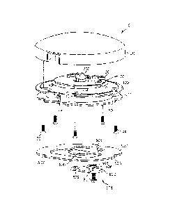
BACKGROUND OF THE DISCLOSURE
[0003] Dental and medical professionals use many instruments that are
controlled by
separate, discrete control devices. For. example, surgical cutting
instruments, ultrasonic
dental scalars, endoscopic tools, irrigation and aspiration tools, dental
drills, air polishers,
other low speed hygiene handpieces, and dental prophylaxis units can be
activated with
foot control systems. The foot control system typically includes a foot pedal
device that is
placed on the floor within easy reach of the practitioner. The foot pedal is
used to activate
a dental/medical apparatus, which includes a base operating unit. The
available foot
pedals include both "hardwired" systems and wireless foot control systems. The
base unit
raay be activated by depressing the foot pedal, which initiates communication
with the
base operating unit. The base operating unit is then in communication with the
instrument, for example, a dental handpiece.
[0004] Such foot pedals need to be robust to withstand rough treatment
that is
encountered by foot-actuated devices, since pressure applied by the foot is
normally
greater than that which is applied by hand-operated devices. Also, the foot
pedal is
normally located on the floor where it may be accidentally kicked, upset, or
otherwise
- 1
CA 02806979 2013-01-29
WO 2011/130221
PCT/US2011/032049
exposed to moving or falling objects. Existing foot pedals are thus typically
equipped
with few electrical or electronic elements, such as spring actuated switches
and position
sensors, which transmit control signals to a remotely positioned controller by
wired
connections. The remotely positioned controller may house less sturdy
electronic
circuitry for controlling wireless communications between the foot pedal and
the medical
or dental instruments that are being remotely controlled by the foot pedal.
[0005] Therefore,
what is needed is a wireless dental hygiene system that is modular,
that includes reduced costs of certain portions, reduces or eliminates
surfaces and/or
regions where undesirable substances may be deposited, and improves capability
for
disinfection. What is also needed is an electronic circuit or circuit board
for
communication between the cordless dental hygiene system components, such as
the foot
pedal and the various hand pieces.
SUMMARY OF THE DISCLOSURE
[0006] One aspect
of the disclosure includes a printed circuit board for a wireless foot
pedal control system. The printed circuit board includes a substrate for
mounting a
plurality of electronic components. The electronic components include a
programmable
controller having a memory for storing software and data; a radio frequency
(RF)
transceiver which = is arranged for wireless communications with at least one
remote
device; an accelerometer; a wake-up device for generating a wake-up signal to
the
controller; and an antenna commnnicatively coupled with the RF transceiver.
The
electronic components are in electronic communication through printed circuit
traces on
the substrate, to control wireless communications between the foot pedal and
one or more
remote wireless devices.
[0007] Another
aspect of the disclosure includes a wireless foot pedal controller for
communication with at least one wireless dental instrument. The wireless foot
pedal
controller includes a housing, a power source and a printed circuit board
positioned
within the housing. The printed circuit board is connected to receive power
from the
power source, and includes an analog to digital signal converter. The printed
circuit
board also includes a substrate for mounting a plurality of electronic
components. The
- 2 -
CA 2806979 2017-04-24
81659460
electronic components include a programmable controller having a memory for
storing
software and data; a radio frequency transceiver which is arranged for
wireless
communications with at least one remote device; an accelerometer; a wake-up
device for
generating a wake-up signal to the controller; and an antenna communicatively
coupled with
the RF transceiver. The electronic components are in electronic communication
through
printed circuit traces on the substrate, to control wireless communications
between the foot
pedal and one or more remote wireless devices.
[0007a] Another aspect of the disclosure includes a wireless dental foot pedal
controller for
communication with at least one wireless dental instrument, comprising: (a) a
housing; (b) a
power source and (c) a printed circuit board positioned within the housing,
the printed circuit
board connected to receive power from the power source; (d) an analog to
digital signal
converter; and the printed circuit board comprising a substrate for mounting a
plurality of
electronic components, the electronic components comprising: (i) a
programmable controller
comprising non-volatile memory for storing software and data; (ii) a radio
frequency for
wireless communications with at least one other remote device; (iii) an
accelerometer
comprising a capacitive sensing cell and a signal conditioning application-
specific integrated
circuit that measures the capacitive sensing cell and extract acceleration
data from a difference
between two capacitors; and outputs a voltage signal that is proportional to
acceleration and
scaled substantially linearly with an applied supply voltage; (iv) a wake-up
device for
generating a wake-up signal to the controller; and (v) an antenna; the
electronic components
in electronic communication through printed circuit traces on the substrate,
to control wireless
communications between the foot pedal and one or more remote wireless devices.
BRIEF DESCRIPTION OF THE DRAWINGS
[0008] Figure 1 is a perspective view of the foot pedal of the present
invention.
[0009] Figure 2 is a partially exploded view of the foot pedal of Figure 1.
[0010] Figure 3 is a fully exploded view of the printed circuit board
assembly, the upper
housing and lower housing of the present invention.
-3 -
CA 2806979 2017-04-24
81659460
[0011] Figure 4 is a top view of the upper surface of the printed circuit
board assembly.
[0012] Figure 5 is a plan view of the lower surface of the printed circuit
board assembly.
[0013] FIG. 6 shows a plan view of the top surface of the printed circuit
board assembly.
[0014] FIG. 7 shows a plan view of the ground plane of the printed circuit
board assembly.
[0015] FIG. 8 shows a plan view of the power plane of the printed circuit
board assembly.
[0016] Wherever possible, the same reference numbers will be used
throughout the
drawings to represent the same parts.
- 3a -
CA 02806979 2013-01-29
WO 2011/130221
PCT/US2011/032049
DETAILED DESCRIPTION OF THE DISCLOSURE
[0017] The present
disclosure now will be described more fully hereinafter with
reference to the accompanying drawings, in which an exemplary embodiment of
the
disclosure is shown. This disclosure may, however, be embodied in many
different forms
and should not be construed as limited to the embodiments set forth herein.
[0018] Figure 1 is
a perspective view of a cordless foot pedal 10 of the present
invention. A cover 20 hides the foot pedal internals from view, although a
charge
connector 22 is visible. Charge connector 22 accepts an electrical cord for
recharging a
battery positioned inside cover 20. Foot pedal 10 sits on a base having a
rubber pad 600
which is spaced from cover 20. Base 600 supports lower housing 500 and upper
housing
400.
[0019] Figure 2 is
a partially exploded view of cordless foot pedal 10, displaying the
internal arrangement within cover 20. Printed circuit board (PCB) assembly
overlies
upper housing 400, which is spaced from lower housing 500. Holding ring 300 is
fastened to cover 20 by fastener 26, and upper surface 404 (FIG. 3) of upper
housing 400
is captured between cover 20 and holding ring 300. Lower housing 500 is
attached to
upper housing 400 and restrained from rotation by anti-rotation fasteners 804,
26. PCB
assembly 100 is attached to upper housing 400 by fastener assemblies 30.
Charge
connector 22 is visible on a wall of upper housing 400. Plunger housing
assembly 700
extends through an aperture in PCB assembly 100. Screws 26 extend through
scallops
502, 402 in lower housing 500 and upper housing 400 and through apertures 302
in
holding ring 300. Screws 26 are captured in corresponding female threaded
regions (not
visible) that may be molded into cover 20. An anti-skid bottom 600 is
adhesively or
otherwise affixed to lower housing 500. Anti-skid bottom 600 includes scallops
602 that
allow anti-skid bottom 600 to be assembled over screws 26 (FIG. 3). Lower
housing 500
may be rotated within upper housing 400 and held in place in lower housing 500
by
corresponding features, such as flanges, not visible in upper housing 400.
Access cover
800 is also visible in Figure 2. Access cover 800 slides into aperture 606 and
into a
mating feature in lower housing 500. Access cover 800 includes a pair of tabs
802 that
extend onto one side of lower housing 500 while screw 804 slides through an
aperture
- 4 -
CA 02806979 2013-01-29
WO 2011/130221
PCT/US2011/032049
808 in lock tab 806 and into a female threaded receiver (not visible) in lower
housing
500, thereby locking access cover 800 in place. Alternatively, lock tab
aperture 808 may
be threaded to capture screw 804. Access cover 800 provides access to the
interior of foot
pedal 10 through aperture 606, and importantly to a bottom surface of PCB
assembly 100
by simply removing screw 804 and sliding access cover 800 from lower housing
500,
without the need to completely disassemble lower housing 500 from upper
housing 400,
in order to provide access to communication test pads on PCB assembly 100.
Cordless
foot pedal 10 is free to move along a floor, and cover 20, as will become
clear, can move
with respect to the remaining portions of the foot pedal 10.
[0020] Figure 3 is
a further exploded view of the upper housing 400, the lower
housing 500 and portions of foot pedal 10 either attached to upper housing 400
and lower
housing 500 or captured within upper housing 400 and lower housing 500.
[0021] Upper
housing 400 is shown having an upper surface 404 and a vertical
surface 406. A charge connector aperture 410 penetrates vertical surface 406
that receives
charge connector 22. Upper surface 404 includes a central aperture 412,
through with
plunger assembly 700 extends. Upper surface 404 also includes a plurality of
female
thread housings 408. Upper surface further includes additional apertures 414,
whose
purpose will be readily apparent below.
[0022] Also shown
in Figure 3 is PCB assembly 100. PCB assembly 100 includes a
plurality of scallops 102 and has an upper surface 104 and a lower surface
106. Upper
surface 104 and lower surface 106 are shown in detail in Figures 5 and 6 and
are further
discussed below. PCB assembly 100 is assembled to upper housing 400 using a
plurality
of fastener assemblies 30. Each fastener assembly 30 comprises a screw 32, a
washer 34
and grommet 36. Each grommet 36 is assembled along the edge of PCB assembly
100 at
each scallop 102. Grommets 36 are then assembled over female thread housings
408, and
washers 34 are assembled over grommets 36 and screws 32 secure fastener
assemblies 30
to 408, thereby securing PCB assembly 100 to upper housing 400.
[0023] Figure 3
also shows lower housing 500, plunger housing assembly 700,
battery 38, charge connector 22 and holding ring 300. Plunger housing assembly
sits on
- 5 -
CA 02806979 2013-01-29
WO 2011/130221 PCT/US2011/032049
lower housing 500, extending through holding ring 300, upper housing central
aperture
412 and PCB assembly center aperture 112. Plunger housing assembly 700
includes two
arms. First arm is a plunger arm 702 while second arm is a potentiometer
coupling arm
704. Also depicted in Figure 3 is a potentiometer adaptor lever 900. Lever 900
includes a
slot 902 and an aperture 904. When assembled, potentiometer coupling arm 704,
plunger
arm 702 and lever 900 are positioned below printed circuit board assembly 100,
even
though a portion of plunger housing assembly 700 may protrude through central
aperture
112. Slot 902 of potentiometer adaptor lever 900 fits over potentiometer
coupling arm
704 of plunger housing assembly 700. Any movement of plunger housing assembly
700
will cause movement of potentiometer coupling arm 704 which will cause
movement of
potentiometer adaptor lever 900 as slot 902 moves with plunger arm 702.
[0024] Also depicted in Figure 3 is battery 38 and charge connector 22. A
first
electrical connector 40 is attached to battery 38 via first wire 42. A second
electrical
connector 50 is also attached to charge connector 22 via a second wire 52.
When
assembled, fastener assemblies 30 attach PCB assembly 100 to female thread
housings
408 in upper housing 400. Screws 26 attach holding ring 300 to cover 20,
capturing upper
housing 400 and holding ring 300. Lower housing 500 is assembled into upper
housing
400 with scallops 502 over screws 26 and rotated. As shown in Figure 3,
rotation is
counterclockwise. On rotation, notched flanges 514 positively engage cross-
members
(not visible) in upper housing 400 to lock lower housing 500 in position with
respect to
upper housing. Charge connector 22 is seated in charge connector aperture 410
by any
convenient means. It may be held in, for example, with fasteners, or it may be
held in
place by a snap-fit. Battery 38 and wires= 42 and 52 reside in the space
between upper
housing 400 and lower housing 500. Tabs may be included on the bottom of upper
housing 400 for wire management for battery wires 42, 52.
[0025] Figures 4 and 5 disclose the upper surface 104 and the lower surface
106 of
printed circuit board assembly 100. Figure 5 depicts the traces that are
characteristic of a
printed circuit board assembly.
[0026] PCB assembly 100 includes a microcontroller 120 which preferably may
include non-volatile memory, e.g., electrically-erasable programmable read-
only memory
- 6 -
CA 02806979 2013-01-29
WO 2011/130221
PCT/US2011/032049
integrated circuit (EEPROM) or an alternative type of non-volatile rewriteable
memory
such as flash memory, a linear single cell lithium ion charger 134, an
impedance track
battery fuel gauge 136, a low noise regulator (not shown), an RS 232
transceiver 138, a
radio frequency (RF) transceiver which may or may not be integrated into
microcontroller 120 (not shown), accelerometer 140, and an antenna 150, which
are in
electronic communication through printed circuit traces on the substrate 170.
Non volatile
memory portion of microcontroller 120 may in various alternate embodiments be
something other than EEPROM, e.g., flash memory, other forms of read-only
memory
that is capable of retaining stored information when power is lost. In at
least one
exemplary embodiment RF transceiver may be a 2.4GHz RF transceiver, and the
antenna
configured for 2.45 GHz antenna transmission. Other receiver and antenna
configurations
may be used, provided that the transceiver and antenna are matched. In the
exemplary
embodiment the transceiver operates over a range of from about 2405 MHz to
about 2480
MHz, and the antenna operates over about substantially the same range. The
transceiver
selects a channel in the range. Broadly stated, RF transceiver and antenna may
be
configured for any RF frequency provided that they are compatibly tuned to the
selected
frequency. The voltage regulator may be preferably configured for 2.5 volts,
although a
voltage regulator for any suitable operating voltage may be used. Also
included on PCB
assembly 100 may be a wake-up switch 160, potentiometer 132, and miscellaneous
circuit elements ¨ resistors, capacitors, inductors, external connectors, test
points, and
voltage suppressors.
[0027]
Microcontroller 120 provides logic control for all of the components and
wireless communications between foot pedal 10 and remotely-controlled devices.
For
example, communications and logic control may include software, hardware and
combinations thereof for synchronizing foot pedal 10 with one or more wireless
dental
handpiece or other dental or medical instruments for selectively pairing and
controlling
the instrument. In at least one exemplary embodiment battery capacity
measuring device
136 may be a System-Side Impedance Track Fuel Gauge, model no. BQ27500DRZT
manufactured by Texas Instruments of Dallas, Texas, or a microcontroller
having
comparable operating characteristics. Any microcontroller known in the art is
suitable
for use herein regardless of amount of flash memory and RAM.
- 7 -
CA 02806979 2013-01-29
WO 2011/130221
PCT/US2011/032049
[0028] Antenna 150
is connected through a balun (not shown) to the transceiver 139
to provide RF input signals to transceiver 139. Antenna 150 is configured for
communications in the appropriate standard, e.g., ZigBee, Bluetooth, IEEE
802.11or
telemetry.
[0029] Transceiver
139 may be, for example in a preferred embodiment, a ZigBeeTM
compliant platform 2.4 GHz low power transceiver plus microcontroller or other
transceiver capable of compliance with IEEE 802.15.4 standard. Transceiver
139 may
be an RF,transceiver which is an 802.15.4 standard compliant radio that
operates in the
2.4 GHz ISM frequency band. Transceiver 139 may include a low noise amplifier,
1 mW
nominal output power, with internal voltage controlled oscillator (VCO),
integrated
transmit/receive switch, on-board power supply regulation, and full spread-
spectrum
encoding and decoding. Transceiver 139 may preferably include a
microcontroller unit,
for example, an 8 bit S08-based microcontroller unit by FreeScale
Semiconductor. Inc.,
i i
of Austin, Texas. In the exemplary embodiment shown n FIG. 4, transceiver 139
s
incorporated into microprocessor, or microcontroller unit 120, however in
alternate
embodiments the transceiver can be separated from microprocessor 120.
Transceiver 139
is preferably located between microprocessor 120 and antenna 150.
[0030] RS232
transceiver 138 provides an electrical interface between an
asynchronous communication controller and the serial-port connector for
handling data
communications, although in an alternate embodiment transceiver 138 may
include a
different type of serial interface, e.g., USB and comparable serial
interfaces.
[0031] An
accelerometer 140 detects when foot pedal 10 is in a level and upright
position to permit operation of foot pedal 10. If foot pedal 10 is tilted or
not upright and
level, i.e., in the intended position for use, controller inhibits any motor
enabling
transmission of signals between the handpiece and foot pedal 10 and keeps foot
pedal 10
from operating the handpiece until it is returned to the proper orientation.
In one
embodiment accelerometer 140 is an integrated-circuit accelerometer.
Accelerometer 140
may also detect vibration in foot pedal 10.
[0032] In an
alternate embodiment, accelerometer 140 may include a capacitive
- 8 -
CA 02806979 2013-01-29
WO 2011/130221
PCT/US2011/032049
sensing cell (g-cell) and a signal conditioning ASIC. The g-cell is a
mechanical structure
formed from semiconductor materials. The ASIC uses switched capacitor
techniques to
measure the g-cell capacitors and extract the acceleration data from the
difference
between the two capacitors. The ASIC also signal conditions and filters the
signal,
providing an output voltage that is ratiometric and proportional to
acceleration.
Ratiometric means that the output offset voltage and sensitivity is scaled
substantially
linearly with applied supply voltage. As supply voltage is increased, the
sensitivity and
offset increase linearly; as supply voltage decreases, offset and sensitivity
decrease
linearly. In an alternate embodiment, the accelerometer 140 may provide a
sleep mode
feature to conserve battery power during extended periods when foot pedal 10
is not in
use. When sleep mode is active, accelerometer 140 outputs are turned off to
reduce of
operating current. When a wake-up signal is received by accelerometer 140, it
resumes a
normal mode of operation.
[0033] In another
exemplary embodiment, accelerometer 140 may also include a self
test feature to permit verification of the mechanical and electrical integrity
of
accelerometer 140. In another embodiment, accelerometer 140 may include plural
sensitivity settings - referred to as g-select settings - which allows for the
selection
between two or more sensitivities. Depending on the a logic input signal,
accelerometer
140 internal gain may be changed to allow it to function, for example, with a
3g or llg
sensitivity. The g-Select option can be omitted if foot pedal 10 requires only
a single,
e.g., 3g, sensitivity.
[0034] A wake-up
switch 160 may be used to detect vertical depression of cover 20
on foot pedal 10, and generate a wake-up signal to the system. In an alternate
embodiment, wake-up switch 160 may also detect tilt and vibration. The signal
level may
be read directly by a digital input and used to interrupt or wake up
microcontroller/EEPROM 120, or counted to estimate the amount and duration of
activity. If foot pedal 10 is not in an upright operating position, for
example if
inadvertently kicked by the operator, foot pedal 10 may be disabled to prevent
accidental
initiation of control signals to one of the associated dental instruments.
While a wake-up
switch is used in the exemplary embodiment, other methods to awaken the system
may
- 9 -
CA 02806979 2013-01-29
WO 2011/130221
PCT/US2011/032049
be used, such as an RF source or accelerometer, or any external energy source
with an
energy sensing transducer.
[0035] Referring
next to FIGS. 5-8, substrate 170 includes a composite of four layers,
a top layer 104 on which components are mounted, a power plane 110 for power
connections, a ground plane 114 for grounding connections, and a bottom layer
106 for
soldering components to substrate 170. Exemplary layers 106, 104, 110, 114,
are
illustrated in FIGS. 5-9. Substrate 170 supports components mounted on top
layer 104
and provides electrical interconnections and external connection points for
the
components. Substrate 170 is generally planar, disk-shaped, with a circular
profile that
conforms generally to the shape of foot pedal 10 housing and aperture 112 to
allow
plunger housing assembly 700 to pass through substrate 170.
[00361 While only
certain features and embodiments of the invention have been
shown and described, many modifications and changes may occur to those skilled
in the
art (for example, variations in sizes, dimensions, structures, shapes and
proportions of the
various elements, values of parameters (for example, temperatures, pressures,
etc.),
mounting arrangements, use of materials, colors, orientations, etc.) without
materially
departing from the novel teachings and advantages of the subject matter
recited in the
claims. The order or sequence of any process or method steps may be varied or
re-
sequenced according to alternative embodiments. It is, therefore, to be
understood that
the appended claims are intended to cover all such modifications and changes
as fall
within the true spirit of the invention. Furtheiniore, in an effort to provide
a concise
description of the exemplary embodiments, all features of an actual
implementation may
not have been described (i.e., those unrelated to the presently contemplated
best mode of
carrying out the invention, or those unrelated to enabling the claimed
invention). It
should be appreciated that in the development of any such actual
implementation, as in
any engineering or design project, numerous implementation specific decisions
may be
made. Such a development effort might be complex and time consuming, but would
nevertheless be a routine undertaking of design, fabrication, and manufacture
for those of
ordinary skill having the benefit of this disclosure, without undue
experimentation.
- 10 -