Note: Descriptions are shown in the official language in which they were submitted.
CA 02807027 2013-02-20
k .
FULL RINGS FOR A FUNCTIONALIZED LAYER INSERT OF AN
OPHTHALMIC LENS
The invention relates to an active layer insert for an ophthalmic device
formed
from multiple functional layers which are stacked and a method for forming the
active
layer insert. More specifically, various designs for full rings that comprise
the
functional layers.
BACKGROUND
Traditionally an ophthalmic device, such as a contact lens, an intraocular
lens
or a punctal plug included a biocompatible device with a corrective, cosmetic
or
therapeutic quality. A contact lens, for example, can provide one or more of:
vision
correcting functionality; cosmetic enhancement; and therapeutic effects. Each
function
is provided by a physical characteristic of the lens. A design incorporating a
refractive
quality into a lens can provide a vision corrective function. A pigment
incorporated
into the lens can provide a cosmetic enhancement. An active agent incorporated
into a
lens can provide a therapeutic functionality. Such physical characteristics
are
accomplished without the lens entering into an energized state. A punctal plug
has
traditionally been a passive device.
More recently, it has been theorized that active components may be
incorporated into a contact lens. Some components can include semiconductor
devices. Some examples have shown semiconductor devices embedded in a contact
lens placed upon animal eyes. It has also been described how the active
components
may be energized and activated in numerous manners within the lens structure
itself.
The topology and size of the space defined by the lens structure creates a
novel and
challenging environment for the definition of various functionalities.
Generally, such
disclosures have included discrete devices. However, the size and power
requirements
for available discrete devices are not necessarily conducive for inclusion in
a device to
be worn on a human eye.
SUMMARY
According to a first aspect of the invention there is provided an active lens
insert for an ophthalmic lens. The lens comprising: annular shaped full ring
substrate
layers with one or both of electrical and logical Functionality; wherein the
size, shape
1
CA 02807027 2013-02-20
and stacking structure of each of the annular shaped substrate layers is based
on the
thickness around an optical zone of the ophthalmic lens; electrical
interconnections
between substrate layers. The active lens insert encapsulated with one or more
materials for bonding within the body material of a molded ophthalmic lens.
The substrate functional layers may be adhered to insulating layers forming a
stacked feature.
The annular shaped full ring substrate layers may be cut from a wafer.
The size, shape and stacking structure of each of the annular shaped substrate
layers may be further based on the base curve of an ophthalmic lens.
The size, shape and stacking structure of each of the annular shaped substrate
layers may be further based on by the diameter of an ophthalmic lens.
The size, shape and stacking structure of each of the annular shaped substrate
layers is further based on by encapsulation parameters of the active lens
insert.
The active lens insert may comprise an encapsulating biocompatible polymer.
The biocompatible polymer for encapsulation may be a polysilicone based
polymer.
The encapsulation of the active lens insert may maintains a minimum thickness
between an edge of a substrate layer and an outer edge of a lens of less than
about 150
micron thickness.
The active lens insert may comprise three or more annular shaped substrate
layers.
The substrate insert may comprise a full ring annular shape.
One or more of the substrate layers of the active lens insert may comprise one
or more individually functionalized layer.
One or more of the individually functionalized layers may comprise a metallic
layer which functions as an antenna.
One or more of the substrate layers of the active lens insert may comprise an
energization source.
One or more of the substrate layers of the substrate insert may comprise power
regulation source.
The power regulation source may comprise at least one semiconductor layer
with electronic microcircuitry capable to control electric current flow from
the
electrochemical cells.
2
CA 02807027 2013-02-20
The electronic microcircuitry may be electrically connected to an
electroactive
lens component within the ophthalmic lens.
The power regulation of one or more substrate layers may be capable of
receiving power from external sources.
The power regulation of one or more substrate layers may be capable of
charging the battery layer.
The power regulation of one or more substrate layers may be capable of
controlling the use of power when the ophthalmic lens is not in a charging
environment.
The power regulation of one or more substrate layers may be capable of
controlling the use of power when the ophthalmic lens is in a charging
environment.
One or more of the substrate layers of the substrate insert may comprise solid
state energy source.
One or more of the substrate layers may comprise microcircuitry to detect
actuation signals for the active lens insert.
According to a second aspect of the invention there is provided a method of
forming an active lens insert for an ophthalmic lens is described. The method
comprising: forming annular shaped full ring substrate layers with one or both
of
electrical and logical Functionality; wherein the size, shape and stacking
structure of
each of the annular shaped substrate layers is based on the thickness around
an optical
zone of the ophthalmic lens; forming electrical interconnections between
substrate
layers; and encapsulating the active lens insert with one or more materials
that may be
bonded within the body material of a molded ophthalmic lens.
The method may comprise adhering the substrate functional layers to insulating
layers to form a stacked feature.
The annular shaped full ring substrate layers may be cut from a wafer.
The size, shape and stacking structure of each of the annular shaped substrate
layers may be further based on the base curve of an ophthalmic lens.
The size, shape and stacking structure of each of the annular shaped substrate
layers may be further based on the diameter of an ophthalmic lens.
The size, shape and stacking structure of each of the annular shaped substrate
layers may be further based on encapsulation parameters of the active lens
insert.
The active lens insert may be encapsulated by a biocompatible polymer.
3
CA 02807027 2013-02-20
a
The biocompatible polymer for encapsulation may be a polysilicone based
polymer.
The encapsulation of the active lens insert may maintain a minimum thickness
between an edge of a substrate layer and an outer edge of a lens of less than
about 150
micron thickness.
The active lens insert may comprise three or more annular shaped substrate
layers.
The substrate insert may comprise a full ring annular shape.
One or more of the substrate layers of the active lens insert may comprise one
or more individually functionalized layer.
One or more of the individually functionalized layers may comprise a metallic
layer which functions as an antenna.
One or more of the substrate layers of the active lens insert may comprise an
energization source.
One or more of the substrate layers of the substrate insert may comprise power
regulation source.
The power regulation source may comprise at least one semiconductor layer
with electronic microcircuitry capable to control electric current flow from
the
electrochemical cells.
The electronic microcircuitry may be electrically connected to an
electroactive
lens component within the ophthalmic lens.
The power regulation of one or more substrate layers may be capable of
receiving power from external sources.
The power regulation of one or more substrate layers may be capable of
charging the battery layer.
The power regulation of one or more substrate layers may be capable of
controlling the use of power when the ophthalmic lens is not in a charging
environment.
The power regulation of one or more substrate layers may be capable of
controlling the use of power when the ophthalmic lens is in a charging
environment.
One or more of the substrate layers of the substrate insert may comprise solid
state energy source.
4
CA 02807027 2013-02-20
One or more of the substrate layers may comprise microcircuitry to detect
actuation signals for the active lens insert.
A functionalized layer insert that can be energized and incorporated into an
ophthalmic device is described herein. The insert may be formed of multiple
layers
which may have unique functionality for each layer; or alternatively mixed
functionality but in multiple layers. The layers may have layers dedicated to
the
energization of the product or the activation of the product or for control of
functional
components within the lens body.
The functionalized layer insert may contain a layer in an energized state
which
is capable of powering a component capable of drawing a current. Components
may
include, for example, one or more of: a variable optic lens element, and a
semiconductor device, which may either be located in the stacked layer insert
or
otherwise connected to it. Some examples may also include a cast molded
silicone
hydrogel contact lens with a rigid or formable insert of stacked
functionalized layers
contained within the ophthalmic lens in a biocompatible fashion.
Accordingly, there is provided a disclosure of an ophthalmic lens with a
stacked functionalized layer portion as well as various designs for rings that
comprise
the functional layers. Full ring designs parameters can include, for example,
thickness,
shape, stacking structure, etc. In some examples, design parameters may be
influenced
by one or more of; the thickness around an optical zone of the lens, the base
curve of
the lens, the diameter of the lens and encapsulation parameters.
An insert may be formed from multiple layers in various manners and placed in
proximity to one, or both of, a first mold part and a second mold part. A
reactive
monomer mix is placed between the first mold part and the second mold part.
The first
mold part is positioned proximate to the second mold part thereby forming a
lens
cavity with the energized substrate insert and at least some of the reactive
monomer
mix in the lens cavity; the reactive monomer mix is exposed to actinic
radiation to
form an ophthalmic lens. Lenses may be formed via the control of actinic
radiation to
which the reactive monomer mixture is exposed.
DESCRIPTION OF THE DRAWINGS
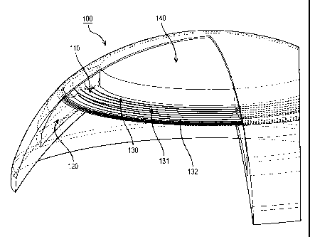
FIG. 1 illustrates a three dimensional section representation of an insert
formed of
stacked functional layers which is incorporated within an ophthalmic lens mold
part.
5
CA 02807027 2013-02-20
FIG. 2 illustrates two cross-sectional representations of inserts formed of
stacked
functional layers incorporated within two different shaped ophthalmic lenses.
FIG. 3 illustrates two cross-sectional representations of inserts formed of
stacked
functional layers incorporated within ophthalmic lenses with different
encapsulation
parameters.
FIG. 4 illustrates two cross-sectional representations of inserts formed of
stacked
functional layers with different layer thicknesses incorporated within
ophthalmic
lenses.
FIG. 5A illustrates a top-down view of a wafer with an arrangement of full
annular die.
FIG. 5B illustrates a top-down close up view of one full annular die with
center cutout.
DETAILED DESCRIPTION
The present invention relates to an active lens insert device formed through
the
stacking of multiple functionalized layers. Additionally various designs for a
wafer
including rings that may be used to make up functionalized layers in a
functional layer
insert, for incorporation into an ophthalmic lens are provided.
In the following sections detailed descriptions of embodiments of the present
invention will be given. The description provides embodiments only, and it is
understood that to those skilled in the art that variations, modifications and
alterations
may be apparent. It is therefore to be understood that said embodiments do not
limit
the scope of the underlying invention.
Glossary
In this description and claims directed to the presented invention, various
terms
may be used for which the following definitions will apply:
Active Lens Insert: as used herein refers to an electronic or
electromechanical
device with controls based upon logic circuits.
Arc-matched (or arc matching): as used herein refers to the design of a Ring
Segment which includes an identical External Radius and Internal Radius, such
that the
curvature of the External Arc matches the curvature of the Internal Arc. Arc
matching
is used to efficiently nest Ring Segments on a Wafer, maximizing wafer
utilization.
6
CA 02807027 2013-02-20
Dicing Street Width: as used herein refers to the width of a thin non-
functional
space between integrated circuits on a Wafer, where a saw or other device or
method
can safely cut the Wafer into individual Die without damaging the circuits.
Die: as used herein refers to a block of semiconducting material, on which a
given functional circuit is fabricated. Die are created on and cut from a
Wafer.
Energized: as used herein refers to the state of being able to supply
electrical
current to or to have electrical energy stored within.
Energy: as used herein refers to the capacity of a physical system to do work.
Many uses within herein may relate to the said capacity being able to perform
electrical
actions in doing work.
Energy Source: as used herein refers to device capable of supplying Energy or
placing a biomedical device in an Energized state.
External Arc: as used herein refers to the external or convex edge of a Ring
Segment, which is a portion of the circumference of the circle defined by the
External
Radius.
External Radius: as used herein refers to the radius of the circle that
defines the
external edge of a Full Ring or Ring Segment. The External Radius determines
the
curvature of the External Arc.
Full Ring: as used herein refers to one complete ring-shaped layer in a
Functionalized Layer Insert. A Full Ring may be comprised of multiple Ring
Segments or may be one Intact Ring.
Functionalized: as used herein refers to making a layer or device able to
perform
a function including for example, energization, activation, or control.
Functionalized Layer Insert: as used herein refers to an insert for an
ophthalmic
device formed from multiple functional layers which are stacked. The multiple
layers
may have unique functionality for each layer; or alternatively mixed
functionality but
in multiple layers. In some examples, the layers are rings.
Intact Ring: as used herein refers to one complete ring-shaped layer in a
Functionalized Layer Insert which is made of a single intact Die.
Internal Arc: as used herein refers to the internal or concave edge of a Ring
Segment. The Internal Arc may, be a single arc segment, the curvature of which
is
determined by the Internal Radius. The Internal Arc may be comprised of
multiple arc
segments of different curvatures, defined by different Internal Radii.
7
CA 02807027 2013-02-20
.4
%
Internal Radius: as used herein refers to the radius of the circle that
defines the
internal edge or a portion of the internal edge of a Full Ring or Ring
Segment. The
Internal Radius determines the curvature of the Internal Arc.
Lens: refers to any ophthalmic device that resides in or on the eye. These
5 devices can provide optical correction or may be cosmetic. For example,
the term lens
can refer to a contact lens, intraocular lens, overlay lens, ocular insert,
optical insert or
other similar device through which vision is corrected or modified, or through
which
eye physiology is cosmetically enhanced (e.g. iris color) without impeding
vision. The
preferred lenses are soft contact lenses made from silicone elastomers or
hydrogels,
10 which include but are not limited to silicone hydrogels, and
fluorohydrogels.
Mold: refers to a rigid or semi-rigid object that may be used to form lenses
from
uncured formulations. Some preferred molds include two mold parts forming a
front
curve mold part and a back curve mold part.
Power: as used herein refers to work done or energy transferred per unit of
time.
15 Ring Segment: as used herein refers to one Die which may be combined
with
other Die to construct a Full Ring. As used in this description, a Ring
Segment is
generally flat and is formed in an arcuate shape.
Stacked: as used herein means to place at least two component layers in
proximity to each other such that at least a portion of one surface of one of
the layers
20 contacts a first surface of a second layer. A film, whether for adhesion
or other
functions may reside between the two layers that are in contact with each
other through
said film.
Substrate insert: as used herein refers to a formable or rigid substrate
capable of
supporting an Energy Source within an ophthalmic lens. The Substrate insert
may also
25 support one or more components.
Wafer: as used herein refers to a thin slice of semiconductor material, such
as
silicon crystal, used in the fabrication of integrated circuits and other
microdevices.
The wafer serves as the substrate for microelectronic devices built in and
over the
wafer and undergoes many microfabrication process steps.
30 Apparatus
Referring now to Fig. 1, demonstrated as item 100 is a three dimensional
representation of an embodiment of the present invention of a fully formed
ophthalmic
8
CA 02807027 2013-02-20
lens using a stacked layer substrate insert formed as a functionalized layer
insert 110.
The representation shows a partial cut out from the ophthalmic lens to realize
the
different layers present inside the device. A body material 120 is shown in
cross
section of the encapsulating layers of the substrate insert. The body material
120 is
contained fully within and extends around the entire circumference of the
ophthalmic
lens. It may be clear to one skilled in the arts that the actual functionalize
layer insert
110 may comprise a full annular ring or other shapes that still may reside
within the
constraints of the size of a typical ophthalmic lens.
Layers 130, 131 and 132 illustrate three of numerous layers that may be found
in a functionalized layer insert 110. A single layer may include one or more
of: active
and passive components and portions with structural, electrical or physical
properties
conducive to a particular purpose.
A layer 130 may optionally include an energization source, such as, for
example, one or more of: a battery, a capacitor and a receiver within the
layer 130.
Item 131 then, in a non limiting exemplary sense, may comprise microcircuitry
in a
layer that detects actuation signals for an active lens insert 140. A power
regulation
layer 132, may be included that is capable of receiving power from external
sources,
charging the battery layer 130 and controlling the use of battery power from
layer 130
when the lens is not in a charging environment. The power regulation layer 132
may
also control signals to an exemplary active lens insert 140 in the center
annular cutout
of the functionalized layer insert 110.
In general, a functionalized layer insert 110 is embodied within an ophthalmic
lens via automation which places an energy source a desired location relative
to a mold
part used to fashion the lens.
The size, shape, and stacking structure of the die that may be used to form
layers such as 130, 131 and 132 in a functionalized layer insert 110 is
influenced by
several factors, as shown in Figs. 2, 3 and 4.
Fig. 2 illustrates the effect of lens shape on the design of a functionalized
layer
insert. The base curve, diameter, and thickness of an ophthalmic lens define a
maximum size and shape of an included functionalized layer insert. Fig. 2
shows, as
one example, the impact of different base curves. Item 200A depicts a cross
sectional
view of a portion of an ophthalmic lens 205A with more curvature than the
ophthalmic
lens 205B, depicted in item 200B, which is flatter. The flatter lens 205B can
9
CA 02807027 2013-02-20
, .
accommodate a functionalized layer insert 201B of greater width 202B, as
compared to
the narrower width 202A of a functionalized layer insert 201A that fits within
lens
205A having greater base curvature. It should be apparent that a lens of
smaller
diameter (203A indicates a lens diameter) would limit the width of a
functionalized
layer insert while a lens with larger diameter would accommodate a wider
functionalized layer insert. Likewise, a lens of less thickness (204A
indicates a lens
thickness) would limit the number of layers in a functionalized layer insert
as well as
the width of a functionalized layer insert, while a thicker lens might support
more
layers and layers of greater width.
Fig. 3 illustrates the effect of encapsulation parameters on the design of a
functionalized layer insert. Encapsulation parameters, such as, by way of non-
limiting
example, maintaining a minimum 100 micron thickness between the edge of a die
and
the outer edge of a lens, affect the size and shape of a functionalized layer
insert and
therefore the size and shape of individual layers. Item 300A depicts a cross-
sectional
view of a portion of an ophthalmic lens 305A with a functionalized layer
insert 301A
and encapsulation boundary 303A. The ophthalmic lens 305B depicted in item
300B
includes a functionalized layer insert 301B and a relatively wider
encapsulation
boundary 303B as compared to boundary 303A which is narrower. It can be seen
that
the wider encapsulation boundary 303B necessitates that the functionalized
layer insert
301B be narrower in width 302B as compared to the functionalized layer insert
301A
with width 302A.
Depicted in Fig. 4 is the effect of functional layer thickness on the design
of a
functionalized layer insert. Item 400A represents a cross-sectional view of a
portion of
an ophthalmic lens 405A with a functionalized layer insert 401A including
three layers
with material, such as, for example, insulating layers, between the functional
layers. A
functionalized layer insert may contain more or less than three layers. The
ophthalmic
lens 405B depicted in item 400B includes a functionalized layer insert 401B
with
relatively thicker layers 402B as compared to the layers 402A in the
functionalized
layer insert 401A which are thinner. The lens curvature in these two examples
allows
the width of the bottom layers 402A and 402B to remain the same. However, it
can be
seen that the increased height of the functionalized layer insert 401B as
compared to
401A, combined with the lens curvature, causes the top layer 402A to be
limited in
width. The thickness of each functional layer impacts other dimensions, such
as
CA 02807027 2013-02-20
functional layer width, that will fit within the required lens and
encapsulation
parameters. Thicker layers within the functionalized layer insert will be more
restricted in other dimensions, such as width, in order to remain within the
confines of
the lens geometry.
The example depicted includes a functionalized layer insert in the shape of a
ring, formed as an intact ring-shaped die.
Full Ring Layout
Referring now to Fig. 5A, depicted is a top-down view of an 8-inch wafer 501A
with a layout including full ring die 502A with center cutout 503A. The figure
shows
the area required for each full ring die 502A, but only illustrates an example
of the
center cutout 503A for one full ring die 502A. Full ring die 502A are
positioned
adjacent to one another, with at least a dicing street width separation
between rings.
The most efficient layout includes full ring die 502A arranged in concentric
circles
around the circumference of the wafer. In this design, significant areas
between the
individual full ring die 502A are not usable, as well as the center cutout
503A portion
of each ring. A layout including full ring die 501A results in inefficient
utilization of a
wafer, producing 255 full rings and utilizing only 25.9% of the wafer
material.
Referring now to Fig. 5B, a top-down close up view of a full ring die 502B is
depicted with center cutout 503B. When the center cutout 503B is removed, the
full
ring die 502B is defined by an outer perimeter 504B and an inner perimeter
505B. The
center cutout 503B is unusable after removal from each full ring die 502B
produced on
a wafer, and is therefore wasted material.
Conclusion
The description above and as further defined by the claims below, provides
various designs for rings that make up the functionalized layers in a
functional layer
insert, for incorporation into an ophthalmic lens.
11