Note: Descriptions are shown in the official language in which they were submitted.
CA 02807056 2013-01-29
WO 2011/112817 PCT/US2011/027915
PROTECTIVE ADHESIVE FILM., METHOD OF ADHERING PROTECTIVE
ADHESIVE FILM TO A DEVICE, ?-\.-ND DEVICE COIVIPRISING PRO 'f EC'TIVE
ADHESIVE FILM
RELATED APPLICATIONS
[0001) This application claims priority to U.S. Non-Provisional AppliCatiall
NO, 13/044,275, entitled,. "Protective Adhesive Film, Method of Adhering
'Protective
Adhesive Film to a Device and Device Comprising Protective Adhesive Filial,"
filed
on March 9, 201 I, which claims priority -to U.S. Provisional Application NO.
61/313,363, entitled "Method of Adhering, a Protective Adhesive Film to a
Device and
Device Comprising Protective .Adhesive Film," .filed on March 12, 2010;
Provisional Application Na. 61./316,185, entitled "Protective Adhesive Film,
Method
of Adhering Protective Adhesive Film to a Device and Device Comprising
Protective
Adhesive .Film," filed. on March 22, 2010; LI,S, Provisional Application No.
61/359,690, entitled "Micro-Matte Protective Film, 'Method of Adhering. Micro-
Matte
Protective Film to a .Device and Device Comprising Micro-Matte Protective
Film,"
filed on Ante 29, 2010; and U.S. Provisional Application No. 6I /44008,
entitled.
"Protective Adhesive Film, Niethod of Adhering Protective Adhesive Film to a
Device and 'De-vice Comprising Protective Adhesive Film," filed on February 8,
2011.
BACKGROUND
E0002) The present .invention relates generally to methods of applying
protective -films to electronic device surfaces and to devices comprising -
protective
100031 Protective films are used to cover and protect a variety of materials
and
devices from, for example, scratches or dents that may he imparted during
transport or
use of the device. Protective films may be .used to protect, .fOr example, the
surface of
digital electronic device components during manufacture, or may be adhered to
a
WO 2011/112817 CA 02807056 2013-01-29PCT/US2011/027915
completed device to protect it flOin damage during nottnal day-to-day use. A
variety
of protective .filins are known,, each having. properties that .may be
advantageous for
some uses and disadvantageous for other uses. One form of protective .film
used in
the. art is coated on one side with a layer of a dry pressure-sensitive
adhesive that has
sufficient tack .to form a secure contact .with the device while permitting
slight
repositioning of the film after adherence. Protective films are often
transparent, and
may permit .the use of touch-sensitive features of the electronic device
through die
100041 Typically, when a dry protective -film, particularly a protective film
having an adhesive layer, is applied to a surface, air is easily trapped
between a device
surface and -the film during application, causing the appearance a bubbles.
Bubbles
are undesirable for aesthetic reasons but also because their presence over an
optical
screen distorts images on a screen viewed by a device user. 'Prior methods of
eliminating trapped air bubbles beneath protective films utilize an aqueous
solution or
other solvent to temporarily reduce adherence between a film and a device,
permitting
trapped air to be forced out by mechanical pressure. Known methods, for
example,
include spraying a protective .film. (or de-vice surface) with water or
another liquid,
applying the wet film to the device surface to he protected (or ;Applying the
film to the
wet device .surface), and using pressure (e,g., with a squeegee) to smooth the
filin and
force out any trapped air bubbles. In doing so, the water or other liquid is
also forced
out frotn between the. film and the device surface, and collects at an edge of
the film,
100051 Thus, prior methods required introduction of a liquid to the outer
surface of a device, requiring a user to take additional steps to remove
liquid after a
-film is applied to a de-vice. A significant disadvantage to using a wet
solution to apply
a protective film -is potential introduction of liquid into an electronic
device, for
-2-
WO 2011/112817 CA 02807056 2013-01-29PCT/US2011/027915
example, through the apertures for the speaker or head set jack. la SOMC
cases, Liquid
entering an interior housing of a device may cause a device to fail, For this
reason,
device manufacturers commonly include nioisture sensitive indicators within
their
devices to help diagnose device failure. In some casesõ a manufacturer vi1l
void a
device's warranty vhere inspection of a device and its .moisture indicators
show
exposure to moisture.
[0006] Another drawback of many protective films is the high visibility of
fingerprints, smudges or other marks on the filmõ 'resulting, ìr example, from
handling of a device. In particular, visibility of 'fingerprints or other
marks on .films
covering. electronic device bodies or display screens is aesthetically and
functionally
undesirable. A visible residue over a display screen, for example., may
distort the
transmission of light .from the screen resulting in distortion of an image
viewed on the.
.screen. Matte surface treatments have been used to .address this problem, but
the
application of typical matte surfaces over an optical screen reduces optical
transmission.
SUMMARY
[00071 in one general aspect, a method of applying a protective film to a
device includes providing a protective film comprising an adhesive layer
covered by a
backing. The adhesive layer is disposed on a first major surface of the
protective
film. The .method further includes removing at least a portion of the backing
to
expose an adhesive area and contacting the exposed adhesive area to a surface
portion
of a portable electronic device. The method further includes applying a
pressure to a
second major stirface of the protective fihn to press the exposed adhesive
layer
against the surface portion of the portable, electronic device. The method may
be
performed without the application of any liquid to the device or the film
_3_
WO 2011/112817 CA 02807056 2013-01-29PCT/US2011/027915
100081 In some embodiments, the adhesive layer comprises a piessure-
sensitive adhesive. The .pressure-sensitive adhesive .may include a copolymer
comprising an acr,,,late polymer and a silicone macromer. 1.n some
embodiments, the.
method includes diffusing air bubbles through the protective film.
[0009] The method may include applying the pressure .with a smoothing
device. In some embodiments,. the pressure may be applied to an exposed
surface of a
cap .sheet, the cap sheet disposed on the second major surface of the
protective film.
In some embodiments., after applying the pressure to the exposed surface of
the cap
sheet, the method includes removing the cap sheet to expose the second major
surface
of the protective film, In some embodiments, after the pressure is applied to
the
second major surface of the protective film, the inethod includes
repositioning the
protective .film.
[00101 The contacting step may include holding the protective adhesive film
by at 10aSt one tab extending from the Iihn. n some eMbodiments, after holding
the
protective adhesive .filin by the at least one tab extending from the film,
the method
includes removing the at least one tab from the polyurethane sheet,
[00.1 .l iia another general aspect, an electronic device comprises a display
surface and a. protective film disposed on the display surface. An adhesive
layer is
disposed between and in contact with at least a. portion of a. first major
surface of the
pruiectïvcfii.ua and the display surface. The protective. film may adhere to
the device
without application o.f any liquid or solvent
1001.2.1 hi some embodiments., the electronic device further includes a bezel
that is aligned along each edge of the display and a housing having a
plurality of
corners and sides, wherein the display- surface may be disposed on the
housine. A
second protective film may be disposed on each corner of the housing, andlor a
third
-4-
WO 2011/112817 CA 02807056 2013-01-29PCT/US2011/027915
protective .film may he disposed on the bezelõA second adhesive layer may be.
disposed between and in contact with at least a portion of a. first major
surface of the
second protective film and each corner of the housing. A third adhesive layer
may be.
disposed between and in contact with at least a portion of a. first major
surface of the
third protective film and the bezel. In some embodiments, the second and third
protective films adhere to the device without application of any liquid or
solvent,
[0013] In some embodiments, the protective film comprises polyurethane. In
some embodiments, at least a portion of a second major surface o.fthe
protective filin
Inay include a micro-matte surface structure. In some eMbOdnneinS, no air
bubbles
are visible beneath the surface of the protective adhesive film. In some
embodiments,
the protective film is air permeable. `.1-he adhesive may include an aciylate
polymer
and a silicone macromer.
[001.41 In yet another aspect, a protective adhesive 'film includes a.
polyurethane sheet and an adhesive layer disposed on at least a portion of a
first major
surface of the polyurethane sheet. The adhesive layer includes a pressure-
sensitive
adhesive that comprises a copolymer comprising an acrylate polymer and a
silicone
.macromer. In some embodiments, the protective adhesive :film is configured to
adhere to a display of an electronic device without the application of any
liquid to the
adhesive layer or the device.
10151 The polyurethane Sheet may be between about 75 microns and about
400 microns in thickness. in some embodiments, the polyurethane sheet
comprises a
polycaprolactone-based aliphatic thermoplastic .urethane. I,n SOInO
embodiments., at
least a portion of a .second major surface of the polyurethane sheet comprises
a micro-
Inane surface structure, In some embodiments, the protective adhesive film
includes
-5-
WO 2011/112817 CA 02807056 2013-01-29PCT/US2011/027915
at least one tab extending from the polyurethane sheet. In some embodiments, a
cap
sheet is disposed on a second major surface of the 'polyurethane sheet.
100161 In some embodiments, the adhesive layer is between about 12 microns
and about 75 tnicrons in thickness. The adhesive may include a copolymer of
the
aerylate polymer and a .silicone macromer side Chin.
BRIEF DESCRIPTION OF THE DRA.W1NGS
[0017] FIG. I illustrates an exemplary adhesive film and a step for applying
an adhesive .film to an electronic device.
100181 FIG. 2 .iliustrates an exemplary additional step 11>r applying an.
adhesive film to an electronic device.
[0019] FIG. 3 illustrates an exemplary additional step for applying an.
adhesive film to an electronic device.
[0020j FIG. 4 illustrates an exemplary additional step for applying an
adhesive .film to an electronic device.
[0021.j FIG-. 5 illustrates an exemplary step for applying a protective
adhesive
film that includes a cap sheet layer to an electronic device.
[00221 FIG. 6 an exemplary additional step for applying a protective adhesive
film that includes a cap sheet layer to an electronic device.
[0023J FRI 7 illustrates an exemplary additional step for applying a.
protective adhesive film that includes a cap sheet layer to an electronic
device.
[00241 FIG. 8 illustrates an exemplary additional step for applying a
protective adhesive 'film that includes a. cap sheet layer to an electronic
device.
DETAILED DESCRIPTION
I0025] As used in the description below and in the appended claims, the.
singular forms "a," "an," and "the" include 'plural references unless the
context clearly
-6-
WO 2011/112817 CA 02807056 2013-01-29 PCT/US2011/027915
dictates otherwise. Unless defined otherwise, all technical and scientific
terMS used in.
this document have the same meanings as commonly understood by one of ordinary
skill in the art. As used in this document, the: term "comprising" means
"including,
but not :limited to." As used herein, the term "about," when referring to a
value,
means plus or minus 10% of the value.
100261 This disclosure is not- limited to the particular systems, devices and
methods described, as these may vary. Also, the terminology used in this
document is
only for the purpose of describing particular versions or embodiments, and it
is not
intend.ed to lirnit the :scope.
10271 Devices and methods are disclosed that avoid the need for an aqueous.
solution or other Iìqi.nd in applying a protective adhesive -film to an
electronic device
and removing trapped .air bubbles. As described herein, a protective film
.comprising
an adhesive layer (e.g., a pressure-sensitive adhesive layer) may be adhered
to 8.
device surface without the use of an aqueous :solution to remove trapped air
'bubbles.
Instead, trapped air bubbles are removed by applying pressnre across the film
surface
to mechanically eliminate large (e.g., greater than 2-3 min in diameter) air
'bubbles,
-while permitting smaller air bubbles to be eliminated over time. The adhesive
film
ma.y be disposed on a -first major surface of the protective adhesive film. As
used in
the document, the, term "major surface" refers to a planar surface of a sheet
or layer of
a film. In general, a sheet -will have two opposing major .surfaces.
[0028l In :some embodiments:, a protective íílna may comprise a -polyurethane
sheet, e.g., a polycaprolactone-based aliphatic thermoplastic -urethane sheet.
A first
major surface of a polyurethane sheet may be coated with one or :more layers
of a
pressure-sensitive adhesive, such as a copolymer comprising an acrylate
polymer and
a silicone macromer. In some enibodiments, the protective film is a
-7-
WO 2011/112817 CA 02807056 2013-01-29PCT/US2011/027915
polycaprolactone-based aliphatic thermoplastic urethane and comprises an
adhesive
layer consisting essentially of a. copolymer of an acrylate polymer and
silicone
macromer side chains. A micro-matte surface structure may be formed on at
least a
second .maior surface of the sheet, as described herein.. In another
embodiment., a
protective =film may comprise a polyurethane sheet, e.g., a polycaprolactone-
based
aliphatic thermoplastic urethane sheet. The sheet may be coated on one side
with a
micro-matte layer, as described herein.
100291 The protective adhesive film may comprise a polyurethane sheet, e.g..,
an aliphatic polyester -urethane-based sheet, e.g. a polycaprolactone based
aliphatic
thermoplastic urethane sheet, coated on all or part of a first major surface
(or
-backed") with an .adilesive layer, in some embodiments, the adhesive layer is
a
pressure-sensitive adhesive layer. The pressure-sensitive .adhesive layer (or
coating)
may be a copolymer comprising an acrylate polymer and a silicone macromer, Ln
some embodiments, an adhesive layer thickness may be about 10 to about
microns, about 12 to about 75 microns, about 25 to about 38 microns, about 30
micro.ns, or about 35 microns. The pressure-sensitive adhesive layer (or
coating) .may
comprise an acrylate-silicone copolymer based pressure-sensitive adhesive. The
adhesive layer ma.y comprise additional components, eg.,a tackifier or
plasticizer,
and may be a. self-healing, adhesive. The adhesive layer may be formed without
the
use of a cross-linker or photo-initiator. The adhesive layer may be prepared
using a
thermal cure process. In some embodiments, the adhesive layer is made of an
adhesive that does not immediately firmly secure, the, film to a device and
thus .allows
for slight repositionability of the film after .placement on tile device. For
example, the
adhesive layer may include an amount of silicone to permit repositionability.
in some.
embodiments, tin-polymerized silicone, tackifier, or other low molecular
weight.
-8-
WO 2011/112817 CA 02807056 2013-01-29
PCT/US2011/027915
components are included in the adhesive layer and migrate into the
polyurethane sheet
:and modify its characteristics, A polyurethane sheet comprising an adhesive
layer
may be made more flexible or more impact resistant by the interaction with one
or
more such components from an adhesive,
[0030] In some embodiments., the adhesive layer comprises a polyacrylate-
based pressure-sensitive adhesive layer, .having silicone macromer side chain
modifications of one or more acrylate ester groups, in some embodiments, the
adhesive layer may be pre-pared from or comprise acrylic acid, metbacrylic
acid.,
esters of acrylic acid comprising 4 to 21 carbon atoms, esters of methacrylic
acid
comprising 5 to 21 carbon atoms, acorlanaide, substituted. .acrylamides such
as N,N-
diniethyl acrylamide, styrene., substituted styrenes such as vinyl toluene,
aerylonitriie,
methacrylonitrile, vìnyl pyrrolidone, N-vinyl caprolactam, vinylidene
chloride,
vinyl esters of carboxylic acids, 2-(2-ethoxyethoxy)ethy1 acrylate, 2-
ethylhexyl
acrylate, butyl acrylaie. hydroxyethyl acrylate, hydroxypropyl acrylate, 2-
carboxyethyl acrylateõ ethoxyethyl acrylate, perfluorooctyl acrylate, isooetyl
acrylate,
divinylbenzeneõ vinylbenzyl chloride, vinyl acetate, glycidyi methacylate,
hydroethyl
acetate, .hydroxypropyl acetate, glacial acrylic acid, methyl acrylate, ethyl
aeryiate,
butyl acrylate, iso butyl acrylate or other acrylates, or combinations
thereof, in some
embodiments, the pressure-sensitive adhesive comprises acrylate and silicone
in other
polymer configurations as known in the art. Suitable pressure-sensitive
adhesives
may be manufactured by 3N4 Company of St, Paul, MN Or other manufacturing.
companies,
[00311 The protective film may have a thickness from about 75 .microns up to
about 400 microns. For example, the protective adhesive films used may have
thicknesses including about 75 microns, about 100 microns, about 1.50 microns,
about
-9-
WO 2011/112817 CA 02807056 2013-01-29 PCT/US2011/027915
.175 microns,. about 200 microns, about 250 microns, about 300 microns., ar
about 350
microns. fierent thicknesses may be used for different parts of a device
example, an electronic device use a. 150 micron, .film for the device's
optical
screen and a 300 Micron fihn for the device's body. Such .films may provide
scratch
resistance, impact resistance, or both, and may provide higher impa.ct
resistance to the
parts of the device that are most likely to need it, while preserving the
sensitivity
and/or clarity of portions of the device that are less likely to require
impact resistance.
100321 The protective adhesive film to be adhered to a device optical screen
may ..have a shore .hardness of between about 85A. and 99A, or between about
50D and.
75D to provide a strong filnsi with a .flat surface with minimal or no surface
distortion
(e.g.. "orange peel"). .1.:n .sorne embodiments, the shore hardness of the
protective
adhesive film is about 60D or about 93A. The protective adhesive film may
allow for
proper optical transmission and may provide a substantially .smooth surface so
that it
best mirrors the glass sm.-Ike on the device. In addition to providing, an
aesthetic
benefit, this allows for minimal or no reduction in sensitivity andlor
connectivity for
touch .screens.
100331 The device body- filMS may have a variety of surface types, including
anti-dare, glossy, or .matte, and may be optically transparent, transparent
with a inane
texture, translucent or opaque. The film may comprise UV absorbers. The films
may
be colored or uncolored. In some embodiments, the protective adhesive film may
comprise a surface having a micro-matte structure.. Surface treatments may
vary over
a single device, i.e,, a film covering 811 optical screen may have an anti-
glare surface.
while filtn co-vering a device body may have a niatte surface.. A portion of a
protective film to be adhered to the body of a device (portions not including
the
optical screen), the optical screen, or both may have a matte andfor ra micro-
matte
WO 2011/112817 CA 02807056 2013-01-29PCT/US2011/027915
'finish or layer \vhich rnay eliminate or reduce fingerprints and adds
additional "grip"
to the device. Suitable protective films may be manufactured by Argotec Inc,
of
Greenfield, MA, or other similar manufacturing companies. In some embodiments,
the adhesive coating or layer may be protected by a removable backing (e.g.,
prior to
adhering the protective film to a device) before die protective adhesive film
is adhered
to a device SUrthee.
[0034] A micro-matte surface stmcture is one that has a matte finish with an
average roughness,. Ra, between about OM um and. about 0.22 gm, or about 0.1.7
WTI,
or about 0.135 p.m. In some embodiments, a micro-matte surface structure has
an
average maximum. height, Ry, between about 0.50 p.m and about 1.20 1.1m, or
about
.1.1.1 um, or about 1,23 p.m, A. micro-matte surface structure may have an
average
depth, Rmax, between about 1.30 um and. about 1.50 um, or about 1.40 pin.
[00351 in some embodiments, a micro-matte protective film is prepared by
extrusion of a urethane resin onto a micro-matte textured casting sheet.
which, in some
embodiments, may be a 'PET multi-layer film, The urethane resin forms a. film
that,
when removed from the, casting sheet, retains a micro-matte surface texture on
one
side (e.g, a second major surface of the protective film) that mirrors the
texture of the
casting sheet. Thus, a film may be prepared by a single casting of urethane,
rather
than by addition of a micro-inatte layer to a 'smooth urethane .film.
Alternatively, a
micro-matte protective film may be prepared as a co-extrusion of at least two
layers.
Accordingly, a micro-matte protective fain may be prepared using .inultiple
.res.ins of
varying hardness such that its micro-matte structure may be harder and/or MOTe
durable as may be required for specific applications. Alternatively, a micro-
matte
layer may be formed on a polyurethane sheet, for example., by extruding a
resin onto a
urethane film and contacting the resin with a micro-matte casting sheet to
form a
WO 2011/112817 CA 02807056 2013-01-29
PCT/US2011/027915
micro-matte surface texture. The micro-matte protective Jilin may comprise a
pressure-sensitive adhesive layer or la.yers, which m.ay be the same or
similar to the
pressure-sensitive adhesive layer or layers described above n some
embodiments,
the .micro-tnalte textured casting sheet is the .same or different than the
cap sheet
described herein. The micro-matte structure irray cover all or part of a
second major
surface of a protective film.
[0036] In some embodiments, a polyurethane sheet coated with a pressure-
sensitive adhesive (e.g.õ to create a protective adhesive .film) may be cut
into
predetermined shapes designed to fit particular portions of digital electronic
devices
including, but not limited to, mobile telephones, personal digital assistants,
.eReaders,
computer notebooks, nethooks, tablets cameras., game consoles., iPods und
other TvIP3
players, navigation devices, and GPS devices. Such devices typically have a
display
.screen and a housing. l'he cut -filni pieces of the protective adhesive film
may be
applied to the screen andlor other portions of the digital device (such as an
edge, side.,
corner or other portion of the housing, andior the bezel) to protect it from
damage,
using methods described in this document. in some embodiments, the fitin may
be
applied to corners, edges andlor sides of the device to -provide a shock-
absorbing,
itnpact-resistant .skin for the device. The cut film pieces may be desi,..!ned
such that
they contain openings to correspond to various device components and thus do
not
block input or output ports, connections, jacks, or entry points for access to
internal
components of the device. The cut film may- be flexible, to permit its
application onto
curved surfaces smoothly without the appearance o.fgaps, wrinkles, or air
bubbles,
[00371 In :some embodiments, the protective adhesive .film includes a cap
sheet (e.g., a casting film andlor a casting sheet). The cap sheet be
disposed on a
second major surface of the protective flint The cap sheet .may be -formed out
of a.
WO 2011/112817 CA 02807056 2013-01-29PCT/US2011/027915
material(s) that is sufficiently rigid that the pressure applied by a
mechanical
smoothing device (e.g., a squeegee ) does not cause the cap sheet or the
.protective film
to deform (e.g., "orange peel"). Further, the cap sheet may withstand an
increased.
pressure from the mechanical s.moothini. device, which may result in reduced
air
bubbles between the protective film and an electronic device. Additioitally,
the cap
sheet may protect the second major surface of the protective film during
manufacture,
transport, andlor .the end-user installation processes. This may provide an
advantage
over secondary applicationfrelease tapes that include a cured liquid for top
coating
(e.g., a polyurethane andior an acrylic material). The secondary
applicationirelease
tapes include an adhesive that may roughen or distort the second major surface
of the
pressure adhesive layer, which may reduce the opt.ical clarity of the
protective film.
10081 ..che cap sheet may be formed out. of polyester. A polyester cap sheet
(ex., a laminating roll) that is about 2 mils thick may have sufficient
rigidity ancl.
flexibility to prevent the cap sheet andfor the protective film from.
deforming.
Additionally, polyester may withstand the extrusion temperature of the
protective film
(e.g, about 320-35(YF). The cap sheet may comprise polyester, polypropylene,
nylon, polyiande, and similar high-temperature .resistant (e.g., able to
resist the
temperature of the protective film extrusion, such as about 320-350F) andlor
high
melt point films e.g., a .melt point greater than the temperature of the
.protective film
extrusion, such as about 320-350"F). The cap sheet may be from about 0,92 mils
(i.e.,
about 24 microns) to about 10 mils thick (i.e., about 254 ailerons). :In some
embodiments, the cap sheet may be about 2 mils (i.e., about 24 .microns)
thick.. The.
cap sheet may be embossed, brushed, or flat, in some embodiments, a. micro-
matte
surface structure is defined in a cap sheet.
WO 2011/112817 CA 02807056 2013-01-29
PCT/US2011/027915
100391 Suitable materials for the cap sheet and protective fiìiì may include.
one or inore of .the following materials (or similar materials) manufactured
by-
Argotec, Inc, of Greenfield., MA (or other .polyurethane manufacturing
companies)!
ARG)THANE aromatic polyethersithermoplastic polyurethane (part numbers
17103, 17200, 18103, 18212, 182.14, 18215, 18233, 18235, 18242, 18247, 18248,
18305, 18411, .18422., 18433, 1.8450-FR, 18452-.FR3, ARGOTHANEtt aromatic
polyesters/thermoplastic .polyurethane (part numbers 19102, 1.9103, 1.9205,
1.9422,
1.9424, 19426, D7101, 273)3, 27370, 28304, 2..9100, 29102, 29213, 29222,
29285,
and/or 29300). ARGOTHA.N.Et aliphatic polyesters. (part numbers 3751 and/or
A.GKR), ARGOTHANEV aliphatic polycaprolactones/thermoplastic polyurethane
(part number 465.10) ARGOTHANEV Waterproof breathable -am/thermoplastic
polyurethane (part numbers TX 540 and/or Tx2)6o), ARGOFLEXO waterproof-
breathable films/thermoplastic polyurethane (part numbers Tx1300, TX1.500,
and/or
Tx2000), and/or A.R.GOTECirti film no, 49522.
[0040j in some embodiments, at least a portion of a surface of the cap sheet
(e.g., a casting .film andior a casting sheet) has a texture (e.g., brushed,
ribs, ridges,
grooves, .raised dots, etc). The textured surface of the cap sheet may be
disposed on
the second. major .surface of the protective film. The textured surface rnay
cause
micro air pockets to form between the textured .surface and the second major
surface
of the .protective ftl.m. The micro air pockets are small air pockets that
form in gaps
between the textured surface and the second major surface of the protective
film. The
micro air pockets may allow the cap sheet to he more easily removed frotn.
the.
pressure-sensitive adhesive layer .(e.g., by reducing, a seal caused by two
substantially -
smooth surfaces). In the alternative, the second .major surface of the
protective an
may include a textured .surface. However., this may decrease the optical
clarity of the
-
WO 2011/112817 CA 02807056 2013-01-29 PCT/US2011/027915
protective film and, therefore, may be less desirable to the end user. ln some
embodiments, the cap sheet has a texture that defines a micro-matte surface on
the
second major surface of the protective film,
[0041J A mechanical smoothing device may be. used to apply a pressure to an
exposed surface of the cap sheet. The cap sheet may allow .fkir the use of a
wider
and/or more rigid mechanical smoothing device during the installation process
as a
result of the rigidity of the cap sheet. For example, the mechanical smoothing
device
may have approximately the same width as the entire electronic device (e.g.,
eReader,
computer notebook.õ tablet., etc.) or a portion of the electronic device (such
as a display
screen) to which the protective adhesive layer is to be applied. Additionally,
the cap
sheet niay be sufficiently rigid. to withstand the. pressure applied by the
mechanical
smoothing device to minimize. resulting damage (e.g,. distortion) to the
protective
adhesive film.. The smoothing device may be formed from a variety a materials,
including a thick, heavy gauge paper (e.g., greater than about 50 mils thick,
between
about 50-150 mils thick, between about 50-90 mils thick, between about 50-80 -
mils
thick, 'between about 60-80 mils thick, or about 70 mils thick), polyvinyl
chloride
acetate (INCA), unplasticized polyvinyl chloride (uPVC)., silicone nthber,
ethylene
propylene dime monomer .(M-class) rubber (EPDM rubber), .andior other semi-
rigid
rubbers, andlor .rigid plastics, such as rigid polyethylene (e,g., HDPE, MDPE,
LDPE), polyvinyl chlorid.e (PVC), andior polypropylene. For example, the
smoothing
device may be fortned frorn silicone rubber andlor EPDM rubber that is about
60 to
90 Shore A durometer in hardness.
[00421 A wider mechanical smoothing device .may provide several
advantages. For example, a wider mechanical smoothing device only needs to be.
applied once (as it may be about the same width as a screen of an eReader.,
etc.),
-
WO 2011/112817 CA 02807056 2013-01-29PCT/US2011/027915
thereby decreasing Mstallat ion time. Additionally, a µvider mechanical
smoothing
device may minimize unintended skewing, repositioning andfor stretching of the
protective adhesive film that may occur as a result of multiple squeegee
applications
(e.g., in different directions Avid) respect to the screen of an eReader,
etc.). A wider
and harder mechanical smoothing device allows the user to apply an increased
downward force/pressure On the cap sheet, .resutting in an increased adherence
of the
protective adhesive film to the electronic device and/or reduced air bubbles
between
the protective adhesive film and the electronic device.
100431 In some embodiments, the protective film includes a body and at least
one tab that extends outwardly fronr the body, in some embodiments, the
protective
.film includes two tabs, .for example, on opposing sides of the protective
film.. The
tabs may be positioned in the middle of each opposing side, or in .any other
position
along the edee of the protective fihn. The tabs may function as grab handles
to allow
a user to :more accurately position the protective .adhesive film and cap
Sheet on the
electronic device and/or to reduce -fingerprints on the protective adhesive
film, In
some embodiments, the tabs include perforations, allowing the user to more
easily
reino-ve the tabs after installation,
100441 FIG, 1 illustrates an exemplary first .step for applying an adhesive
film
(e.a., a protective adhesive -film andlor a micro-matte protective film) to an
electronic
device. In this step, a portion of a backing layer 20 is -removed Roiri an
adhesive film
to expose an adhesive area 30. The adhesive area 30 is disposed on at least a
portion of a first .major surface 40 of the: protective adhesive .film 10.
Prior to
removing the backing layer 20, the adhesive .film 10 may be modified 'by
elating (e.g.,
by die .cutting, plotter cutting, or other methods) to create segments matched
in size
and shape: to chosen .surface areas on a .particular device to be protected,
-16-
WO 2011/112817 CA 02807056 2013-01-29PCT/US2011/027915
Alternatively, the adhesive =film 10 may be pre-cut to match a desired area on
an
electronic device.
It)) 451 Referring to FIG, 2, after the backing layer 20 is partially or lidly
removed, the adhesive area 30 may be positioned to contact and align with an
exposed
surface portion 50 of an electronic device 60 (e.g., a display surface). In
some
embodiments, the exposed surface portion 50 may be a .small, large, or an
entire.
portion of an exposed surface 70 of the electronic device 60, In .sorne
embodiments,
:the adhesive film 10 andlor the adhesive area 30 are aligned to the
:electronic device
60 (e.g., aligned to the surthce portion 50, e.g., an edge of the exposed
surface 70).
For example, openings 75 in the adhesive film 10 may be aligned to
corresponding
components 65 (e.g., input andior output ports, buttons, etc.) of the
electronic device
60. In some embodiments, prior to contacting the adhesive film. 1.0 to the
electronic
device 60, at least a portion of the exposed surface 70 of the electronic
device may be
cleaned, for example, by rubbing or polishing, the at least a. portion of
exposed surface
70 with a dry tissue or towelette.
100461 The film 10 (e.g.., a protective. adhesive film arid/or a micro-matte
protective film) .may be applied to the electronic device 60 "as is." There is
no need
to apply any liquid or other additive to any portion of the exposed surface.
70 or the
adhesive area. 30 at any time during the .process.
100471 As illustrated in Fla 3, after the film 10 is aligned to the device 60,
the backing layer 20 is completely removed from the first major .sarthce 40 of
the film
10, and the remaining adhesive area 30 of the .film 10 is aligned. to contact
the device
60.
I00481 Referring to FIG, 4, a mechanical smoothing device 100 (e.g., a
squeegee, a device having a resilient edge, or a hand) .may be used to apply a
pressure
-l'7-
WO 2011/112817 CA 02807056 2013-01-29
PCT/US2011/027915
to the second major surface 90 of the -Min 10. The pressure may cause the
adhesive
area 30 to press against the exposed surface portion 50 of the electronic
device 20. In
some embodiments, the mechanical smoothing device 100 applies the pressureli-
om
central area 105 to an. edge 110 of the second major surface 90 continuing in
different
radial directions from the central area 105 across the .second major surface
90. In.
some embodiments:, the mechanical smoothing device 1.00 applies the pressure
starting at or near a trapped air pocket or an air bubble and continues to an
edge .1.1Ø
Any haze or re.maining, trapped air bubbles, if less than about 2-3 mm in
diameter,
may be left to diffuse out. through the protective adhesive film 10 (e.g.õ an
air-
permeable an), generally disappearing within 2.4 hours.
[0049j In .some embodiments, the method may include repositioning the. film.
(e.g., a protective adhesive film andlor a micro-matte protective film) alter
it has
been ad.hered to the exposed surface portion 50 of the device 20. For
example., the
method may- include lifting a portion of the fil.m.10 away from the exposed
surface
portion 50 of the device 20 and reapplying (e.g., re-contacting) the portion
to the
exposed surface portion 50 of the device 20, which -may be helpful in
repositioning
andSor re-aligning the .film 10 andior in removing air bubbles. In some-
embodiments,
additional mechanical smoothing (e.g., by hand or with a mechanical device)
inay be
used to ensure that the film 10 is adhered to the edges II0 of the device 20,
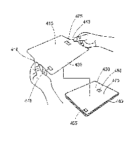
100501 FIGS. 5-8 illustrate an alternative -procedure that may be used for
larger electronic devices, such as tablets., notebooks, and notebooks. In this
embodiment, the protective adhesive film includes a cap sheet layer (e.g., a
casting
andlor a casting sheet). Referring to FIG.. 5, a portion of a backing layer
420 is
removed .from an adhesive film 410 to expose an adhesive area 430. In some
embodiments, the adhesive film 410 is a micro-matte protective adhesive film..
The
-1.8-
WO 2011/112817 CA 02807056 2013-01-29PCT/US2011/027915
adhesive area 430 is disposed on at least a portion of a .first major surface
440 of the
protective adhesive film 410. A cap sheet 510 is disposed on a second .major
surface
of the ..protective adhesive film 410. Prior to removing the backing layer
420, the film.
410, together with the cap sheet 5111 as one piece of separately .from the cap
sheet 510,
may be shaped by cutting (e.g., by die cutting., plotter cuttini4, or other
methods) to
create segments., with a cap sheet 5.10 layered on the adhesive film 41.0,
matched in
size and shape to chosen surface areas on a particular dev.ice to be
protected.
Alternatively, the protective adhesive film 410 and cap sheet 510 may- be pre-
cut to
match a desired area on an electronic device.
100511 After the adhesive is exposed, FIG, .6 illustrates that the adhesive
area
430 may be contacted to an exposed surface portion 450 of an electronic device
460
(e.g., a display .surface). In some embodiments, the exposed surface -portion
450 may
be any portion (yf exposed surface 470 including the entire exposed surface
47Ø In
some embodiments, the adhesive film 410 .andlor the .adhesive area 430 ma.y be
positioned to contact and align with an exposed surface portion 450 of the
electronic
device 460, For example, openings 475 in the adhesive film 411) may be aligned
to
corresponding components 465 (e.g., input and/or output ports, buttons, etc.)
of the
electronic device 460. In some embodiments, at least one optional tab 415
extends
from the adhesive film 410. A user may hold the at least one optional tab 415
while
positioning, contacting, andlor ahuining the adhesive area 430 to the exposed
surface
portion 450 of .the electronic device 460. In some embodiments, prior to
contacting
the adhesive film 410 to the electronic device 460, at least a portion of
exposed
surface 470 of .the electronic device may be cleaned, for example, by rubbing
or
polishine, the at least a portion of exposed surface 470 with a dry tissue or
towelette.
-19-
WO 2011/112817 CA 02807056 2013-01-29PCT/US2011/027915
la some embodiments, no liquid or other additive is applied. to the adhesive
film 411.0õ
the. adhesive area 430, andfor the electronic device .460..
I00521 Referring to FIG. 7, a mechanical smoothing,. device 500 (e.g., a
squeegee, oversized squeegee, a de-vice having a resilient edge, or a hand)
'may be
used to apply a pressure. to the cap sheet 510 disposed on a second .major
surface 490
of the íIn 41Ø The pressure may causes the adhesive area 430 to press
against the
exposed surface portion 450 of the electronic device 460 as depicted in. HO.
6). The
mechanical smoothing device 500 .may be applied starting at an edge 515 of the
electronic device 420 and proceeding across the width 520 of the electronic
device
420. An optional sec.ond mechanical smoothing step may be applied in the
opposite
direction of the first mechanical smoothing:, step. After pressure is applied
with the
mechanical smoothing device 500, the cap sheet 5.10 is removed (e.g., peeled
off) to
expose the second major surface 490 of the film 410, as illustrated in FIG. 8,
Any
haze or remaining trapped air bubbles, if less than about 2-3 min in
diameter., may be
left to diffuse out through the protective adhesive film 410 (e.g., an air-
permeable
ftlm), generally disappearing 1:vithin 24 hours. For example, air bubbles may
diffuse
into theill..rst major surface 440 of the film 410 and out the second major
surface 490
of the film 410. In some embodiments:, after the mechanical smoothing step,
the
optional hold. tabs 415 may be removed from the film 410 by pulling along
optional
perforations (riot shown) or by cutting off the hold tabs 415.
[0053) The method improves the adherence of the film to the surface of the
device, and provides a higher quality (e,g., less damaged, more transparent,
andior
more accurately placed) protective Mtn. The method further reduces the number
of
remaiuing trapped air bubbles. The method further reduces the installation
.time of
applying a protective film to an electronic .device.