Note: Descriptions are shown in the official language in which they were submitted.
WO 2012/058554 CA 02808314 2013-02-13PCT/US2011/058310
UNIVERSAL NETWORK INTERFACE DEVICE BASE MODULE
CROSS-REFERENCE TO RELATED APPLICATIONS
[01] This application is based upon and claims the benefit of priority from
United
States Provisional Application Nos. 61/407,578 filed October 28, 2010,
61/411,489 filed
November 9, 2010 and 61/542,578 filed October 3, 2011 in the United States
Patent and
Trademark Office, the disclosures of which are incorporated herein in its
entirety by
reference.
BACKGROUND
1. Field
[02] The invention is related to a universal network interface device base
module
which can easily installed.
2. Related Art
[03] AT&T's u-Verse and Verizon's FiOS installations require significant
work by
installation crews to reconfigure the home wiring in order to provide service.
One
installation crew will need to connect a drop to the customer residence, and
install an optical
network terminal (ONT) for fiber-based services or install filters in a
network interface
device (NID) for very high bit rate digital subscriber line (VDSL)-based
services. A second
installation crew will then need to work inside the customer residence
establishing a high data
rate pathway to the modem/gateway and reconfigure existing home cabling to
provision
service from the modem/gateway to the point-of-use. Although this methodology
ultimately
provide high quality service to the customer, it is labor-intensive and
expensive for the
service provider.
[04] Additionally, this technical approach is service provider dependent.
If a
customer makes the decision to switch service, the home cabling will need to
be configured
1
WO 2012/058554 CA 02808314 2013-02-13 PCT/US2011/058310
from a new home network topology. This "rewiring" is even more time consuming
and even
more expensive for the service provider.
[05] Therefore, there is a need for an universal modular modem gateway
that may
meet some of the following objectives: 1. Provide a common base platform for
installer; 2.
provide a common form factor for the access module (primary service
provider/customer
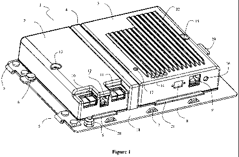
premise interface/media conversion); 3. provide a common form factor for the
modem
module; 4. provide a centralized point from which to distribute signals into
the customer
residence; and 5. provide a clear/simple methodology for technology/platform
upgrades.
[06] Wireless telephony demand continues to increase in the United
States and
abroad. With the introduction new higher bandwidth wireless protocols, such
as, 3G and 4G,
and corresponding introduction of feature rich smart phones, wireless service
providers are
under continual market pressure to increase wireless coverage and bandwidth.
[07] The current method to increase wireless coverage is to add new cell
towers
and the corresponding backbone to support the increased wireless demand.
Although this
approach replicates the existing wireless infrastructure, this approach is
capital intensive and
slow to implement.
SUMMARY
[08] Exemplary implementations of the present invention address at least the
above
problems and/or disadvantages and other disadvantages not described above.
Also, the
present invention is not required to overcome the disadvantages described
above, and an
exemplary implementation of the present invention may not overcome any of the
problems
listed above.
[09] A first embodiment of a universal network interface device base module
includes a universal network interface device base module with an access
module; a modem
2
WO 2012/058554 CA 02808314 2013-02-13 PCT/US2011/058310
module electrically connected to the access module; a dividing structure
placed between the
access module and the modem module; and a base plate; wherein the access
module, modem
module and dividing structure are mounted on the base plate.
[10] The embodiment of a universal network interface device base module may
include a cable connecting said access module to said modem module.
[11] The embodiment of a universal network interface device base module may
include a dividing structure with an opening through which the cable passes.
[12] The embodiment of a universal network interface device base module may
include a dividing structure with a first detent on a first surface facing the
access module and
a second detent on a surface facing the modem module; the access module having
a first
recess on a surface facing the first surface of the dividing structure, such
that the first detent
fits into the access module first recess when the access module is mounted on
the base plate;
and the modem module has a first recess on a surface facing the second surface
of the
dividing structure, such that the second detent fits into the modem module
first recess when
the modem module is mounted on the base plate.
[13] The embodiment of a universal network interface device base module may
include a base plate with a plurality of flanges that abut surfaces of the
access module and
modem module.
[14] The embodiment of a universal network interface device base module may
include a base plate with at least one hinge assembly that can be used to
mount the network
interface device in an enclosure.
[15] The embodiment of a universal network interface device base module may
include an access module that is a one-line xDSL module.
[16] The embodiment of a universal network interface device base module may
include an access module that is a two-line xDSL module.
3
WO 2012/058554 CA 02808314 2013-02-13 PCT/US2011/058310
[17] The embodiment of a universal network interface device base module may
include an access module that is a GPON module.
[18] The embodiment of a universal network interface device base module may
include a modem module that is a wireless modem module.
[19] The embodiment of a universal network interface device base module may
include a dividing structure that has a T-shape.
BRIEF DESCRIPTION OF THE DRAWINGS
[20] Figure 1 shows an isometric view of an embodiment of a uNID base module.
[21] Figure 2 shows a plan view of an embodiment of a uNID base module.
[22] Figure 3 shows a side view of an embodiment of a uNID base module.
[23] Figure 4 shows a transparent view of an embodiment of a uNID base module.
[24] Figure 5 shows a transparent isometric view of an embodiment of a uNID
base
module.
[25] Figure 6 shows an isometric view of an embodiment of a uNID access
module.
[26] Figure 7 shows a schematic of an embodiment of a one line uNID access
module.
[27] Figure 8 shows a schematic of an embodiment of a two line uNID access
module.
[28] Figure 9 shows a schematic of an embodiment of a gigabit-capable passive
optical network (GPON) uNID access module.
[29] Figures 10a and 10b show top and bottom isometric view of an embodiment
of
a uNID Modem Module.
[30] Figure 11 shows a schematic of an embodiment of an uNID modem module.
[31] Figure 12 shows an isometric view of an embodiment of a uNID modem
module on uNID base plate.
4
WO 2012/058554 CA 02808314 2013-02-13 PCT/US2011/058310
[32] Figure 13 shows a side isometric view of an embodiment of a uNID modem
module on uNID base plate.
[33] Figure 14 shows an embodiment of uNID base module attached to a NID base.
[34] Figure 15 shows a plan view of an embodiment of a uNID base module
installed on hinge plate assembly in a NID.
[35] Figure 16 shows an isometric view of an embodiment of a uNID base module
installed on hinge plate assembly in a NID.
[36] Figure 17 shows an isometric view of an embodiment of a uNID base module
on hinge plate assembly.
[37] Figure 18 shows an isometric view of an embodiment of a uNID base module
on open hinge plate assembly.
[38] Figure 19 shows a bottom view of an embodiment of a uNID access module.
[39] Figure 20 shown a side view of an embodiment of an access module.
[40] Figure 21 shows an end view of an embodiment of an access module.
[41] Figure 22 is a system diagram of a typical FTTN / xDSL network.
[42] Figure 23 is a functional diagram of an embodiment of a wireless uNID
base
module.
[43] Figure 24 is a plan view of an embodiment of a wireless uNID base module.
[44] Figure 25 is an isometric view of an embodiment of a wireless uNID base
module.
[45] Figure 26 is an isometric view of an embodiment of a wireless uNID base
module.
[46] Figure 27 is a cross-sectional view of an embodiment of a wireless uNID
base
module.
[47] Figure 28 is an isometric view of an embodiment of a wireless access
module.
5
WO 2012/058554 CA 02808314 2013-02-13 PCT/US2011/058310
[48] Figures 29a, 29b and 29c are top, side, and bottom views of an embodiment
of
a wireless access module for a wireless uNID base module.
[49] Figures 30 shows an isometric view of an alternate embodiment of a uNID
base module.
[50] Figure 31 shows a transparent isometric view of an alternate embodiment
of a
uNID base module.
DETAILED DESCRIPTION
[51] The following detailed description is provided to assist the reader in
gaining a
comprehensive understanding of the methods, apparatuses and/or systems
described herein.
Various changes, modifications, and equivalents of the systems, apparatuses
and/or methods
described herein will suggest themselves to those of ordinary skill in the
art. Descriptions of
well-known functions and structures are omitted to enhance clarity and
conciseness.
[52] Hereinafter, the exemplary embodiments will be described with reference
to
accompanying drawings. If the components are the same in different drawings,
the same
item numbers are used to the extent possible for ease of reference.
[53] Figure 1 shows an isometric view of an embodiment of a universal NID
(uNID) base module 1. Figure 2 shows a plan view of an embodiment of a uNID
base
module. Figure 3 shows a side view of an embodiment of a uNID base module. The
uNID
based module 1 includes three sub-components: a uNID access module 2; a uNID
modem
module 3; and a uNID base plate 18, which includes a dividing structure 4. The
uNID access
module 2 and uNID modem module 3 and dividing structure 4 can be field
attached and
removed from the uNID base plate 18. There are several uNID access module
variants,
including, but not limited to: a one-line xDSL (whenever xDSL is referred to
in the
specification, it could include any one of ADSL, VDSL, VDSL2, or other type of
DSL)
6
WO 2012/058554 CA 02808314 2013-02-13PCT/US2011/058310
access module; a two-line xDSL access module; and a GPON access module. Figure
1 shows
the xDSL variant of access module. There are several uNID modem module
variants,
including, but not limited to: a one-line xDSL modem module; a two-line xDSL
modem
module; and a GPON modem module.
[54] A threaded ground stud 6 is mounted to the uNID base plate 18. The uNID
access module 2 printed circuit board 119 (PCB) (all variants) and uNID modem
module 3
PCB 120 are grounded to the uNID base plate 18 when attached / installed. The
uNID base
module 1 is designed to be installed in a customer premise on an inside wall
(controlled
environment) or on a mounting bracket in a NID that is installed either in a
customer premise
interior (controlled environment) or customer premise exterior (outside plant
environment).
[55] The access module 2 can have several inputs, such as two IDC connectors
10,
11 (one which is connected to a premise and one which is connected to a
telephone
company), an RJ-31 input 12 (which can be used for an alarm). Alternatively,
an RJ-45 may
be used in place of an RJ-31 to install residential alarms. The access module
2 has a
mounting hole 13, through which a screw 69 can be inserted to attach the
access module 2 to
the uNID base plate 18.
[56] The modem module 3 can have an input, such as a RJ-45 input (which is
connected to a premise) 9. It may also have modem status lights 14 and a power
connection
(if power-over-Ethernet is not available) 16. The modem module 3 can also have
a cutout 8
for an SC connector for a GPON modem. The modem module 3 can also have a power
jack
16, such as for 12 vDC. The modem module 3 can have fins 22, which help cool
the modem
module 3. The modem module 3 has a mounting hole 15, through which a screw 74
can be
inserted to attach the modem module 3 to the uNID base plate 18. The modem
module 3 has
an access hole 17 for a tool to be used to disengage the retention clip on the
mating plug 60
for the RJ-45 jack 30.
7
WO 2012/058554 CA 02808314 2013-02-13 PCT/US2011/058310
[57] The uNID base plate 18 includes a pair of hinge assemblies 5, which allow
the
uNID base plate 18 to be mounted and swung in an enclosure. uNID base plate 18
may
include a keeper/retention bracket 6, which is temporarily removed or loosened
and rotated
approximately 90 degrees counter clockwise in order for the uNID base plate 18
to be
mounted on hinges in an enclosure and re-attached/rotated after the uNID base
plate 18 is
mounted in the enclosure. The keeper/retention bracket 6 prevents accidental
removal of the
uNID base plate 18. Without the keeper/retention bracket 6, uNID base plate 18
could easily
become dislodged and slip off the enclosure hinges when uNID base plate 18 is
swung by the
technician in the field, thereby causing damage to the underlying components
below. The
uNID base plate 18 cannot be installed or removed with keeper/retention
bracket 6 in place.
[58] uNID base plate 18 includes several lance type tie down features 7 that
can be
used for wire/fiber management devices. uNID base plate 18 includes flanges
20, 21 and 24,
which help keep the access module 2 and modem module 3 in place. Flange 24
also provides
additional thermal mass to the plate to help sink heat from the modem module
3. uNID base
plate 18 includes a flange/handle 19, which allows the technician to more
easily swing the
uNID base plate 18 when it is in an enclosure. uNID base plate 18 includes a
retention bolt
23 which is used to attached the uNID base plate 18 to an enclosure so that it
cannot swing.
[59] Figure 4 shows a transparent view of an embodiment of a uNID base module.
Figure 5 shows a transparent isometric view of an embodiment of a uNID base
module. The
uNID access module 2 (all variants) and the uNID modem module 3 (all variants)
are
connected with a cable, such as a CAT 7 cable 26. This cable is housed
internally within the
uNID base module 1. Each end of cable 26 has a RJ-45 connector 60, which can
be inserted
into the RJ-45 interconnects 29 and 30. The uNID access module 2 and uNID
modem
module 3 have holes 28 and 27, which can be used to mount the printed circuit
boards 191,
120 in the respective modules to the uNID base plate 18 with bolts/studs 32
and 32, for
8
WO 2012/058554 CA 02808314 2013-02-13 PCT/US2011/058310
example. Figure 5 shows that the dividing structure 4 has an opening 31,
through which
cable 26 extends. Dividing structure 4 can be made of plastic or any other
suitable material,
such as aluminum casting.
[60] While the embodiment shown in figures 4 and 5 show a cable 26 for
connecting the two modules, the two modules could also be electrically
connected by any
commonly know board to board connectors. If a board to board connectors are
used, the use
of the dividing structure would be optional.
[61] Figure 6 shows an isometric view of an embodiment of a uNID access module
2. There are three uNID access module variants: one-line xDSL access module;
two-line
xDSL access module; and GPON access module. The two-line xDSL access module
variant
is shown. The side of uNID access module 2 contains two detents 34 and 35.
Detents 34 and
35 line up with keys/locators/protrusions 73, as shown in figure 13. It is the
combination of
these detents 34, 35 and the flanges 20, 24 on uNID base plate 18 that help
locate the uNID
access module 2 in the correct position so that when the module has been slid
along the
flange and butts against dividing structure 4, the mounting screw 69 is
properly aligned and
ready for securing the modules to the tapped hole in the uNID base plate 18.
Since the
tapped holes in the swing frame plate are underneath the modules it is
difficult to know where
the hole is when attempting the start the screw into the hole as this is a
"blind type" mount
and the method discussed above helps eliminates any guess work as to screw
hole location.
[62] Figure 7 shows a schematic of some of the features of an embodiment of a
one
line uNID access module. They include IDC connector 37 (from the telephone
office); RJ-31
input 38 (alarm); Power-Over-Ethernet (not shown); RJ-45 interconnect 42 (CAT
7 cable to
modem module); IDC connector 39 (to premise). Other components include: POTS /
xDSL
Splitter 41 (POTS (DC to 4 kHz)) and xDSL (25 kHz to 8.5 MHz) ¨ other xDSL
band plans
possible); switchable voice module (SVM), which controls voice switching
between POTS
9
WO 2012/058554 CA 02808314 2013-02-13PCT/US2011/058310
and VoIP, and half-ringer (HR) 40. Other possible options include: switch to
place SVM in-
line or bypass SVM; and SVM status LEDs. Multiple variants are possible due to
number of
VDSL band plans.
[63] Figure 8 shows a schematic of some of the features of an embodiment of a
two
line uNID access module. They include IDC connector 43 for lines 1 and 2 (from
the
telephone office); RJ-31 input 38 (alarm); power-over-Ethernet (not shown); RJ-
45
interconnect 42 (CAT 7 cable to modem module); IDC connector 44 for lines 1
and 2 (to
premise (bi-directional)). Other components include: POTS / xDSL Splitter 41
(POTS (DC
to 4 kHz) and xDSL (25 kHz to 8.5 MHz)) ¨ other xDSL band plans possible);
switchable
voice module (SVM), which controls voice switching between POTS and VoIP, and
half-
ringer (HR) 40; POTS / xDSL Splitter 46 (POTS (DC to 4 kHz) and xDSL (25 kHz
to 8.5
MHz)) ¨ other xDSL band plans possible); switchable voice module (SVM), which
controls
voice switching between POTS and VoIP, and half-ringer (HR) 45; Other possible
options
include: switch to place SVM in-line or bypass SVM; and SVM status LEDs.
Multiple
variants are possible due to number of xDSL band plans.
[64] Figure 9 shows a schematic of some of the features of an embodiment of a
gigabit-capable passive optical network (GPON) uNID access module. They
include SCAPC
bulkhead 47 (single-fiber single mode input)( other connectors could be used
(SCUPC,
LCAPC, LCUPC, etc.); power-over-Internet (not shown); RJ-45 interconnect 52
(CAT 7
cable to modem module). Other components include: WDM 48 (1310/1550 shown with
1550
downstream and 1310 upstream, 1310/1490+1550 (tri-band WDM possible));
transmitter
laser 53 and controller/modulator 56 (upstream transmitter); receiver
photodiode 49 and
controller/demodulator 50 (downstream receiver); input/output (I/O) Bus 51
(memory buffer
not shown); microprocessor/CPU 55 (overall controller). Other design options
include
10
WO 2012/058554 CA 02808314 2013-02-13PCT/US2011/058310
GPON status lights. Multiple variants are possible due to number of PON
variants (B-PON,
GE-PON, etc.).
[65] Figures 10a and 10b show top and bottom isometric view of an embodiment
of
a uNID modem module 3. uNID modem module shown is cast aluminum. Other
materials
may be used as needed based on modem heat generation. A grid pattern 103 is
formed into
the bottom of the uNID modem module 3 to facilitate heat transfer to the uNID
base plate 18.
In addition an interconnect cable pocket 57 is shown. The side of uNID modem
module 3
contains two detents 58 and 59. Detents 58 and 59 line up with
keys/locators/protrusions
similar to keys/locators/protrusions 73 that are on the opposite side of
dividing structure 4, as
shown in figure 13. It is the combination of these detents 58, 59 and the
flanges 21, 24 on
uNID base plate 18 that help locate the uNID access module 3 in the correct
position so that
when the module has been slid along the flange and butts against dividing
structure 4, the
mounting screw 74 is properly aligned and ready for securing the modules to
the tapped hole
in the uNID base plate 18. Since the tapped holes in the swing frame plate are
underneath the
modules it is difficult to know where the hole is when attempting the start
the screw into the
hole as this is a "blind type" mount and the method discussed above helps
eliminates any
guess work as to screw hole location.
[66] Figure 11 shows a schematic of some of the features of an embodiment of a
uNID modem module 3. They include a power-over-Ethernet or power jack 117; CPU
113
with memory 111 (such as flash and RAM); GigE/Phy Bus 115; a power regulating
filter
116; a POTSNoIP relay and control 112; broadband access termination element
114, which
can support ADSL/ADSL 2+, VDSLNDSL2+, SHDSL bonded, and GPON; a RJ-45
interconnect 110 (for connection to the uNID access module 2); and RJ-45
connector 118 (to
premise).
11
WO 2012/058554 CA 02808314 2013-02-13PCT/US2011/058310
[67] Figure 12 shows an isometric view of an embodiment of a uNID Modem
Module on uNID base plate 18.
[68] Figure 13 shows a side isometric view of an embodiment of a uNID modem
module on uNID base plate 18.
[69] Figure 14 shows an embodiment of uNID base module attached to a NID base
61. The uNID base plate hinges 5 are attached to hinges 62 on the NID base 61.
A typical
NID base 61 will have several openings 63 and 64 through which cables can be
attached to
the uNID access module and uNID modem module. A typical NID base 61 may also
have
gas protectors 65 provide lightning surge protection.
[70] Figure 15 shows a plan view of an embodiment of a uNID base module
installed on hinge plate assembly in a NID 61 with a cover 66.
[71] Figure 16 shows an isometric view of an embodiment of a uNID base module
installed on hinge plate assembly in a NID.
[72] Figure 17 shows an isometric view of an embodiment of a uNID base module
on hinge plate assembly.
[73] Figure 18 shows an isometric view of an embodiment of a uNID base module
on open hinge plate assembly. The uNID base plate 18 defines two interior
compartments.
The upper compartment is the area above the uNID base plate 18. The lower
compartment
67 is the area below the hinge plate assembly and a surface of the NID. This
lower
compartment can serve as a storage area where a secondary module, such as a
satellite TV
interconnect Box, can be installed, or other components can be stored.
[74] Figure 19 shows a bottom view of an embodiment of a uNID access module 2.
Screws/bolts 32 are used to attach a printed circuit board 119 to the access
module housing.
These screws/bolts 32 mechanically and electrically (ground) join the uNID
access module
lid, printed circuit board 119, and uNID base plate 18. It also shows the bolt
69 that is used
12
WO 2012/058554 CA 02808314 2013-02-13PCT/US2011/058310
to attached the uNID access module 2 to the uNID plate 18. Depression 70 is a
location for a
product identification label.
[75] Figure 20 shown a side view of an embodiment of a uNID access module 2.
It
shows standoffs 71 and 72 which keep the printed circuit board 119 in place.
[76] Figure 21 shows an end view of an embodiment of a uNID access module 2.
[77] Figure 22 is a system diagram of a typical FTTN / xDSL network. An
Ethernet service switch 75 (such as an Alcatel-Lucent 7450) is installed in a
central office
and connected to a fiber optic backbone F 1 cable. The Ethernet service switch
75 transmits
voice, data/internet, and video content downstream to the ISM FTTN system 76
(such as the
Alcatel-Lucent 7330), and receives voice and data/internet service content
upstream from the
ISM FTTN System. The ISM FTTN system 76 is connected to the service area
interface 78
(SAI) by a copper F2 trunk. The ISM FTTN system 76 transmits voice,
data/internet, and
voice content in an xDSL format to and receives voice, and data/internet
content in a DSL
format from specific F2 copper lines at a service area interface cabinet.
Power is also
supplied to the service area interface 78 by a 190 VDC power supply 77.
[78] A number of copper F2 twisted pair lines are assigned a specific
universal
modem/gateway 84. At least one, but typically two, twisted pair lines are
designed to carry
both voice, data, and video content in an xDSL and DC power. The DC power is
used to
power the universal modem/gateway 84. At least one, but possibly two, twisted
pair lines are
designed to carry DC power to the wireless radio 79 connected to the universal
modem/gateway 84. This DC power is provided by a modem with the ISM FTTN
system but
could be provided by a separate unit.
[79] The universal modem/gateway 84 performs the following functions. It
provide a demarcation point between the landline telephony network and the
wireless
network. It separates DC power from xDSL signal in access module, and provides
front end
13
WO 2012/058554 CA 02808314 2013-02-13PCT/US2011/058310
filtering of bidirectional DSL signal to and from the modem. Power and xDSL
information is
provided to the modem module 80 via an internal interconnect cable. It also
provides a
means to combine modem Ethernet input/output and addition power lines to the
wireless
radio 79 using a single cable. A example of a wireless radio 79 is the Alcatel-
Lucent
Metrocast 9364. It also provides a means to install ancillary equipment near
the wireless
radio 79. The universal modem/gateway also includes gas protectors 84 to
provide lightning
surge protection to the access module 80 and modem module 81. A power/Ethernet
cross-
connect block 82 combines modem input/output cable and additional power lines
into a
single cable.
[80] Figure 23 is a functional diagram of an embodiment of a wireless uNID
base
module. The uNID base module includes the following. A uNID access module 85.
A two
line uNID access module 85 is shown with the input coming through IDC
connector 89. A
one-line version could be implemented based on carrier need. The uNID access
module 85
separates DC power from xDSL signal for both lines (93). The uNID access
module 85
provides front-end filtering of the xDSL signal (91, 92). The uNID access
module 85
provides a single output through a RJ-45 connector 94 to the uNID modem module
86 with
up to two xDSL lines and up to two DC power lines.
[81] Gas protectors 87 provide lightning surge protection to the uNID access
module 85 and uNID modem module 86.
[82] uNID modem module 86 provides communication to/from the ISM FTTN
system and to/from wireless radio, from RJ-45 connector 90. The uNID modem
module
includes a power supply/power regulator 96; CPU 98 with memory 97 (such as
flash and
RAM); GigE/Phy Bus 99; a broadband access termination element 100, which can
support
ADSL/ADSL 2+, VDSL/VDSL2+, SHDSL bonded, and GPON; a RJ-45 interconnect 95
(for
connection to the uNID access module 85).
14
WO 2012/058554 CA 02808314 2013-02-13PCT/US2011/058310
[83] The power/Ethernet cross-connect block 88 combines modem input/output
cable and additional power lines into a single cable.
[84] Figure 24 to 26 show views of an embodiment of a wireless uNID base
module 101 in a NID. uNID access module 102 and uNID modem module 3 are
installed on
a uNID base plate 18. The uNID base plate 18 is attached to the NID by hinges
as discussed
above. Gas Protectors 65 are installed at the bottom center of the NID for
easy connection to
ground wires and the uNID access module 102. A power/Ethernet cross-connect
block 88 is
installed in the lower right-hand corner of the NID.
[85] Typical cable routing configuration is as follows: Input copper cables
enter
the NID in one or both of the left-hand entry ports. This cable is routed
clockwise around the
box. The pairs carrying the xDSL signal and DC power are connected to the gas
Protectors.
A ground wire is connected to the stud 6 on the uNID base plate 18 that both
gas protectors
are connected to.
[86] A twisted pair jumper is connected from the gas protector posts to the
uNID
access module 102 input IDCs. An interconnect cable connects uNID access
module 102 and
uNID modem module 3.
[87] The modem input/output is routed clockwise and connects to the
power/Ethernet cross-connect block. The input cable pairs carrying dc power
only are routed
clockwise around the NID and connected to the power/Ethernet cross-connect
block.
The radio Ethernet cable enters the NID in the lower right-hand corner. This
cable is
routed counter-clockwise around the NID and is connected to the Power/Ethernet
Cross-
Connect Block.
[88] Figure 27 is a cross-sectional view of an embodiment of a wireless uNID
base
module in a NID.
15
WO 2012/058554 CA 02808314 2013-02-13PCT/US2011/058310
[89] Figure 28 is an isometric view of an embodiment of a wireless uNID access
module 102. It is similar to uNID access module 2. However, it has only one
IDC
connectors 104.
[90] Figures 29a, 29b and 29c are top, side, and bottom views of an embodiment
of
a uNID wireless access module.
[91] Figures 30 shows an isometric view of an alternate embodiment of a uNID
base module. It has a T-shaped dividing structure 109 in place of dividing
structure 4.
[92] Figure 31 shows a transparent isometric view of an alternate embodiment
of a
uNID base module.
[93] Advantages and benefits of the invention include the following:
= Common base plate, access module, and modem module Form Factor ¨ this
minimizes manufacturing design variation and reduces cost.
= Modularity.
= Modules can be easily replaced / changed out by service provider
installation
technicians. This provides an easy means for service providers to replace
defective modules
or replace installed modules with new or upgrade modules.
= Centralized home network management point. System provides for installers
to provision service from one point.
= Technology supports copper and fiber based solutions by using different
uNID
access modules and a common uNID modem module.
= When a uNID base module is installed in a NID, the mechanical design
allows
for co-installation of other technologies. For example, a satellite TV
junction box can be
installed in the NID. This option is necessary in rural areas that many have
high speed
internet service but insufficient bandwidth to provide video service.
= Common architecture for network planners.
16
WO 2012/058554 CA 02808314 2013-02-13PCT/US2011/058310
= Modular access modules ¨ one or two line Variants.
= Base platform can be used in landline or wireless applications.
= Low-cost means to use a landline FTTN network as backbone for wireless
service.
[94] Although a few exemplary embodiments of the present invention have been
shown and described, it would be appreciated by those skilled in the art that
changes may be
made in this embodiment without departing from the principles and spirit of
the invention,
the scope of which is defined in the claims and their equivalents.
17