Note: Descriptions are shown in the official language in which they were submitted.
CA 02809592 2013-03-15
DC-AC INVERTER WITH SOFT SWITCHING
Field
This invention relates to DC/AC inverters with soft switching.
Background
Power switches in many DC/AC inverter designs are hard switched, which
generates
EMI noise and losses in the inverter. A low switching frequency may be used to
increase the
inverter efficiency, however, this imposes a compromise in the size of the
inverter components.
Electricity produced by power generators such as photovoltaic (PV)
installations is
becoming increasingly promising as a source of renewable energy. Maximizing
efficiency of
such systems is critical to their widespread utility. One route to improving
efficiency of such
systems is through improving inverter design, and much attention has been
focused on
implementation of micro-inverters; that is, inverters associated with
individual power generators
such as individual PV panels. Conventional approaches to improving efficiency,
such as use of a
low switching frequency, may not be suitable for micro-inverter applications.
Summary
Provided is a DC-AC inverter, comprising: at least one voltage source inverter
circuit or
at least one current source inverter circuit having a DC input and an AC
output including a first
component at a fundamental frequency and a ripple component at a frequency
higher than the
fundamental frequency; wherein the ripple component is of a sufficient
magnitude that the
voltage source inverter circuit output current reverses polarity and allows
the at least one inverter
circuit to operate with zero voltage switching; or wherein the ripple
component is of a sufficient
magnitude that the current source inverter circuit output voltage reverses
polarity and allows the
at least one inverter circuit to operate with zero current switching.
- 1 -
CA 02809592 2013-03-15
One embodiment further comprises a cancellation circuit that substantially
maintains the
ripple component at the inverter circuit output and substantially prevents the
ripple component
from being delivered to a load. The cancellation circuit may comprise a n-
order filter, wherein n
is 2 or more. In one embodiment the cancellation circuit comprises a 3rd-order
filter.
In one embodiment the DC-AC inverter is a voltage source inverter, and the
cancellation
circuit comprises one or more additional voltage source inverter circuits,
each voltage source
inverter circuit providing an AC output including a first component at a
fundamental frequency
and a ripple component at a frequency higher than the fundamental frequency;
wherein outputs
of each voltage source inverter circuit are connected in parallel.
In another embodiment the DC-AC is a current source inverter, and the
cancellation
circuit comprises one or more additional current source inverter circuits,
each current source
inverter circuit providing an AC output including a first component at a
fundamental frequency
and a ripple component at a frequency higher than the fundamental frequency;
wherein outputs
of each current source inverter circuit are connected in parallel or series.
In these embodiments, soft switching may be provided by variable dead time
control of
switches in the at least one voltage source inverter circuit or in the at
least one current source
inverter circuit.
In certain embodiments, outputs of the voltage source inverter circuits or
current source
inverter circuits may be phase shifted by an amount selected to substantially
prevent the ripple
component from being delivered to the load.
In these embodiments, the DC input is provided by a renewable energy source.
The DC
input may be provided by a photovoltaic source. The load may be a power
distribution grid.
Also provided is a photovoltaic module comprising a DC-AC inverter as
described
herein.
Also provided is a power generation system, comprising: a DC-AC inverter as
described
herein, wherein the load is a power distribution grid; and a power generator
that provides the DC
to the inverter circuit.
Also provided is a DC-AC inverter method, comprising: operating at least one
voltage
source inverter circuit or at least one current source inverter circuit such
that an AC output
- 2 -
CA 02809592 2013-03-15
includes a first component at a fundamental frequency and a ripple component
at a frequency
higher than the fundamental frequency; wherein the ripple component is of a
sufficient
magnitude that (i) the voltage source inverter circuit output current reverses
polarity; or (ii) the
current source inverter circuit output voltage reverses polarity; and using
the ripple component to
operate the at least one voltage source inverter circuit with zero voltage
switching; or using the
ripple component to operate the at least one current source inverter circuit
with zero current
switching.
The method may further comprise substantially maintaining the ripple component
at the
inverter circuit output and substantially preventing the ripple component from
being delivered to
a load. The method may further comprise using a n-order filter, wherein n is 2
or more. The
method may further comprise using a 3rd-order filter.
In an embodiment wherein the DC-AC inverter is a voltage source inverter, the
method
may further comprise providing one or more additional voltage source inverter
circuits; operating
each voltage source inverter circuit such that an AC output includes a first
component at a
fundamental frequency and a ripple component at a frequency higher than the
fundamental
frequency; and connecting outputs of each voltage source inverter circuit
together in parallel.
In an embodiment wherein the DC-AC inverter is a current source inverter, the
method
may further comprise providing one or more additional current source inverter
circuits; operating
each current source inverter circuit such that an AC output includes a first
component at a
fundamental frequency and a ripple component at a frequency higher than the
fundamental
frequency; and connecting outputs of each current source inverter circuit
together in parallel or
series.
The method may further comprise using variable dead time control to implement
soh
switching of switches in the at least one voltage source inverter circuit or
in the at least one
current source inverter circuit.
The method may include phase shifting outputs of the voltage source inverter
circuits or
the current source inverter circuits by an amount selected to substantially
prevent the ripple
component from being delivered to the load.
- 3 -
CA 02809592 2013-03-15
The method may comprise connecting a DC input of the DC-AC inverter to a
renewable
energy source, such as a photovoltaic source.
The method may comprise connecting an output of the DC-AC inverter to a power
distribution grid.
Brief Description of the Drawings
For a greater understanding of the invention and to show how it may be carried
into
effect, embodiments are described below, by way of example, with reference to
the
accompanying drawings, wherein:
Figure 1 is a schematic diagram of a conventional full-bridge inverter;
Figure 2A is a simplified schematic diagram of an embodiment of a single phase
inverter
with a 3rd order output filter, wherein the application is a grid-connected PV
panel;
Figure 2B is a simplified diagram of an embodiment of a single phase inverter
with a
higher order output filter, wherein the application is a grid-connected PV
panel;
Figure 3A is a block diagram of a multiple phase voltage source inverter
according to one
embodiment wherein the application is a grid-connected PV system;
Figure 3B is a block diagram of a multiple phase current source inverter
according to one
embodiment wherein the application is a grid-connected PV system;
Figure 4 is a plot showing the effect of output inductance L on switching
ripple in a full-
bridge inverter module, wherein L = 10 mH (top), L = 5 mH (2nd from top), L =
2 mH (3rd from
top), and L = 1 mH (bottom);
Figure 5 is a generalized plot showing zero voltage switching at turn on of a
power
switch of an inverter module;
Figure 6 is a plot showing simulation results of output current ripple for a
single inverter
(igrid_o) and for a phase staggered multiple phase inverter including five
inverter modules,
wherein i grid is the output current when i LI-5 are the output inductor
currents of parallel inverter
modules 1-5, respectively;
- 4 -
CA 02809592 2016-11-01
Figure 7 is a plot showing simulation results of output current ripple for a
single inverter
_grid(0)) and for a phase staggered multiple phase inverter including four
inverter modules,
wherein igrid is the output current when IL] - 1L4 are the output inductor
currents of parallel
inverter modules 1-4, respectively;
Figure 8 is a plot showing simulation results of output current ripple for a
single inverter
(i_grid(o) and for a phase staggered multiple phase inverter including four
inverter modules,
wherein (grid is the output current when IL] - iLs are the output inductor
currents of parallel
inverter modules 1-5, respectively;
Figure 9A is a plot showing operation waveforms of a soft-switched inverter,
according
to one embodiment;
Figures 9B-9H are diagrams showing different states of an inverter circuit
during soft
switching, according to one embodiment;
Figure 10 is a plot showing a dead time generation technique for the leading
edge of the
gate signals for the switches of a leg of a full bridge inverter module,
according to one
embodiment;
Figure 11 is a block diagram of a current control loop according to one
embodiment;
Figure 12 is a plot of simulation results using the control loop of Figure 10
showing the
effect of the feed forward branch in the control loop structure;
Figure 13 is a plot showing simulation results for a multiple phase inverter
with n = 10
full-bridge inverter modules, according to one embodiment, wherein ZVS at
switch turn on is
shown for the switches Si, S2, S3, S4 (from top to bottom);
Figures 14A-14D arc plots showing experimental results for a multiple phase
inverter
embodiment with n = 10 full-bridge inverter modules, for a fixed dead time of
100 ns (Figure
14A) and for variable dead times of 170 ns, 250 ns, and 700 ns (Figures 14B-
14D, respectively);
and
Figure 15 is a plot comparing efficiency of a multiple phase inverter
embodiment under
fixed and variable dead time control.
- 5 -
CA 02809592 2013-03-15
Detailed Description of Embodiments
The circuits and methods provided herein include single phase and multiple
phase
DC/AC inverters in which soft switching is implemented. By implementing soft
switching, i.e.,
zero voltage switching or zero current switching, switching losses are
minimized and efficiency
is improved. Adaptive variable dead-time is used to provide soft switching
under all operating
conditions. Since soft switching as described is based on control algorithms,
no auxiliary circuits
are required for implementation, and hence there is substantially no increase
in cost, component
count, or size associated with implementation.
Embodiments are described herein primarily with respect to full-bridge
inverter topology.
However, implementation in other inverter topologies is contemplated herein,
and those of
ordinary skill in the art will readily understand how to implement the
described embodiments in
other inverter topologies. Further, embodiments are described herein primarily
with respect to
voltage source inverter topologies. However, implementation in current source
inverter
topologies is contemplated herein. Those of ordinary skill in the art will
readily understand how
to implement the described embodiments in current source inverter topologies.
An exemplary full-bridge inverter circuit is shown in Figure 1, and includes a
DC source
Vd, switches Sl-S4, each shown with their body diodes Dl-D4 and drain-source
capacitors Cl-
C4, output inductor L, and load, in this example a power distribution grid.
Inverter circuit and method embodiments provide a large current ripple at the
inverter
output, such that the inverter output current changes its polarity, thereby
enabling the inverter to
operate with soft switching. However, because of the large current ripple at
the inverter output,
the embodiments include passive or active features that reduce or
substantially eliminate ripple
in the current supplied to the load. For example, where the load is a power
distribution grid, the
passive or active features that reduce or substantially eliminate ripple
ensure that the current is
suitable for delivery to the grid, for example, by satisfying standards for
limits for harmonics and
total harmonic distortion (THD) of current supplied to the grid. Passive
features that reduce or
substantially eliminate ripple in the current supplied to the load include an
output filter, as
provided in single phase inverter embodiments. Active features that reduce or
substantially
eliminate ripple in the current supplied to the load include connecting a
number (n) of inverter
modules together in a parallel arrangement, in multiple phase inverter
embodiments.
- 6 -
CA 02809592 2013-03-15
Examples of single phase inverter embodiments are shown in Figures 2A and 2B.
In
these embodiments, a power generator 2, for example a photovoltaic (PV)
generator, produces a
current Ipv that is fed to a DC/AC circuit 4. As described above, the output
current Iirn, of the
DC/AC circuit 4 includes a large current ripple, such that the output inverter
current changes its
polarity, thereby enabling the inverter to operate with zero voltage
switching. The embodiment
of Figure 2A includes a 31" order output filter LI, C, L2, whereas the
embodiment of Figure 2B
includes a higher order output filter 6. The output filters passively reduce
or substantially
eliminate ripple in the current /grid supplied to the load, in this case a
power distribution grid.
Referring to Figure 2A, L1 is selected so that the current 1",õ has enough
ripple for the
worst case scenario, i.e., operation at full output power with sufficient
ripple to ensure that the
current changes polarity. Full power is worst case because the peak of the
fundamental
component of the output current can be too large so that the current with the
ripple does not
reach zero and does not change its polarity. That is, if the peak magnitude of
the current (i.e., the
peak of the sine wave) is too large, the peak to peak ripple at that instant
may not cross zero and
hence there will be no change in polarity. This approach may be used for any
other output filter
design, as shown generally in Figure 2B, provided that the polarity of kõ,
changes every
switching cycle for all operating conditions. This ensures zero voltage
switching in the inverter
circuit. The resulting ripple in the inverter output current Ifm, is higher
than that provided by
conventional designs. This ripple, which may be at one or more harmonic of the
grid frequency,
is reduced or substantially eliminated by appropriate selection of output
filter elements, e.g., C
and L2 in the embodiment of Figure 2A, or elements in a higher order filter as
in Figure 2B,
according to methods well-known in the art. Inductor L1 is selected such that
the output current
ripple level is maintained at the desired value to guarantee soft switching.
Embodiments of generalized multiple phase voltage source and current source
inverters
are shown in Figures 3A and 3B, respectively, as applied to a PV systems. In
the embodiment of
Figure 3A, n parallel-connected voltage source inverter module outputs supply
power to the
utility grid, whereas in the embodiment of Figure 3B, n parallel-connected
current source
inverter module outputs supply power to the utility grid. In another
embodiment, a multiple
phase current source inverter includes n series-connected cun-ent source
inverters. In Figures 3A
and 3B, PV1, PV2, and PVn are the PV panels, and INV I , INV2, and INVn are
the inverter
modules.
- 7 -
CA 02809592 2013-03-15
In the embodiment of Figure 3A, there are two output inductors for each
inverter module,
designated 1,11, and L2õ where n indicates the inverter module to which the
inductors belong. In
some embodiments other configurations of output filter elements may be used.
For example,
there may be only a single output inductor for each inverter module. In other
embodiments of
Figures 3A and 3B, an additional output filter, for example, a higher order
output filter, may be
connected to the combined output of the n inverter modules. See, for example,
Figure 3B.
Referring to the embodiment of Figure 3A, each inverter module includes
features as
described in respect of the embodiments of Figure 2A or 2B; that is, the
output currents kn,/,
of the inverter modules include a large current ripple, such that each
inverter output current
changes polarity, thereby enabling each inverter INV1, 1NV2, INVn to operate
with zero voltage
switching. Similarly, the inverter modules of the embodiment of Figure 3B
include features such
that each inverter module operates with soft switching.
In multiple phase embodiments, the minimum number of inverter modules may be
as few
as two, and the maximum may be determined as a function of the required output
power.
Although there is no theoretical limit on the maximum number of inverter
modules that may be
employed, a practical limit, based on cost or on the need to synchronize the
modules, may be 20
or 30 modules. As used herein, the term "inverter module" refers to a single
inverter circuit,
such as a single full-bridge or a single half-bridge inverter. Multiple phase
embodiments may
also be referred to herein as "interleaved" embodiments.
In multiple phase embodiments, the size of the output filter may be reduced,
relative to
conventional designs, without increasing the switching frequency. Interleaving
improves the
quality (e.g., reduces output current harmonics and THD) of the current fed to
the load. This is
of particular relevance in applications where the inverter output is connected
to the utility grid.
Such applications may include, for example, inverters used in power generation
applications,
such as with photovoltaic (PV), wind turbine, fuel cell, and the like, also
referred to as
distributed generation systems. However, whereas inverters as described herein
may be well-
suited to such applications, they are not limited thereto and may be used in
any application
wherein DC/AC conversion is required.
Thus, as described above, enhanced inverter perfoiniance, including improved
efficiency,
may be obtained by applying soft switching and adaptive variable dead-time
control to a single
- 8 -
CA 02809592 2013-03-15
inverter module or to a number n of inverter modules, wherein the outputs of
the n inverter
modules are connected to a load.
Principle of Operation
The inverter, or the inverter modules of a multiple phase inverter, may be
controlled by a
pulse width modulation (PWM) strategy, such as, e.g., unipolar pulse width
modulation
(UPWM), bipolar pulse width modulation, or selective harmonic cancellation,
using modulating
signals. In a multiple phase inverter, control includes carrier signals phase-
shifted by 0 = 7t/n.
The modulating signals for each inverter module may be substantially
identical.
Each inverter switch (e.g., MOSFET) is operated such that the switching ripple
in the
inductor current is large enough to cause the polarity of the inductor current
to reverse. As a
result, the body diode of the switch conducts the reverse current and produces
a diode voltage
drop (e.g., 0.7 V). Accordingly, the switch turns on at substantially zero
voltage. The effect of
output inductance L on the switching ripple in the switch current is shown in
Figure 4 for four
values of L. At a particular value of the output inductance (e.g., 1 mH in
Figure 4), the ripple is
large enough to cross 0 V and to create a soft switching condition at switch
turn on, as shown in
Figure 5. As a result of soft switching at switch turn-on, switching losses
are minimized.
In accordance with multiphase embodiments described herein, since the outputs
of the
inverter modules are connected together in parallel, the total output current
is the sum of the
currents of the individual modules. For best results, the number n of inverter
modules is selected
to ensure soft switching at substantially every switching period of the
inverter module switches,
including the zero crossings of the current (at line frequency, e.g., 50 Hz or
60 Hz). The ripple
content and the harmonic cancellation in the current fed to the load (e.g.,
the grid) by the n
inverter modules are regulated by controlling the phase shifts 0 between
carrier signals delivered
to each inverter module from a controller. An advantage of such embodiments is
that parallel or
series connection of the inverter module outputs to construct the total output
current allows the
size of the inverter output filter to be reduced. For example, the size of the
output filter may be
reduced to one-tenth of the size required by inverters based on conventional
techniques.
- 9 -
CA 02809592 2016-11-01
By controlling phase-shifts 0 between carrier signals, the n inverter modules
generate n
non-repetitive output current patterns that, upon addition through connection
of the inverter
module outputs, produce a high-quality current waveform. This results from the
effective
switching frequency being n times higher than the actual frequency of
switching and harmonic
cancellation, due to the phase-shift in the carrier signals of the inverter
modules. To realize a
total output power P using n inverter modules and an effective switching
frequency offsõ,,,g; the
contribution of each inverter will be P/n and the actual switching frequency
will be f;,,õ = fmeff n.
The ripple in the sum of the output currents of the n inverter modules is
reduced by a
factor of n. For example, comparison of the inductor current waveform of one
module and that
of the sum of the inductor currents of five modules is shown in Figure 6.
Here, i grid _O represents
the output (e.g., grid) current when no interleaving is implemented, and /grid
is the current fed to
the grid when iL7..5 arc the output inductor currents of parallel inverter
modules 1-5, respectively.
Simulation results for four parallel inverters and for five parallel inverters
are shown zoomed-in
in Figures 7 and 8, respectively, to verify the selection of phase shift angle
0 for even and odd
numbers of parallel inverter modules.
To further reduce switching losses, soft switching at switch turn off may be
implemented.
For example, a snubber capacitor may be used to further reduce switching
losses by providing
substantially zero voltage at turn off. In the presence of the snubber
capacitor, the switch current
decreases with a constant di/dt and the rise of voltage to the input DC
voltage Vd is slowed
down. With a fixed dead time, the switch may not achieve zero voltage
switching under some
conditions because the current might not be great enough to discharge the
snubber capacitor.
From a reliability viewpoint, a long dead time assures that overlapping of the
upper and lower
switch gate drive signals in a leg of the bridge (i.e., in the case of a full-
bridge inverter) will not
occur; however, during the dead-time, the current must continue to flow
through the body diode
of a lower switch of a leg of the bridge (i.e., S2 or S3 in Figure 1) when it
is turned off. Since
this switch has a higher voltage drop, this situation results in higher power
dissipation compared
to the resistive power dissipation when the switch is on.
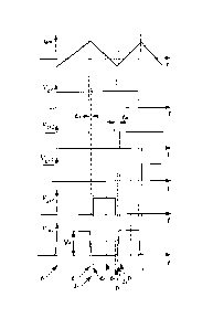
Operation of the inverter is further described with reference to Figures 9A
and 9B-9H.
The inverter operation in steady state can be divided into two modes depending
upon the polarity
of the output voltage Vim', i.e., Vinv>0 or V,nv<0. The stages of operation
for the mode Vinv>0 are
- 10-
CA 02809592 2016-11-01
explained below. Equivalent circuits for the circuit operation are illustrated
in Figures 9B-9H
and the corresponding waveforms are shown in Figure 9A.
Interval 1: In this stage, Si, Sz are on and S3, 54 are off. The inductor
current increases
linearly from a negative value to a peak positive value for to<t<ti (the peak-
to-peak value is
dependent upon the inductance L value). Voltage across the capacitor C2 is 0
while the voltage
across the capacitor C4 is Vd.
Interval 2: 52 turns off when the inductor current is a maximum positive
value. At this
time, the capacitor C2 charges while C4 discharges until the diode D4 is
turned on.
Interval 3: In this interval from t2<t<t3, the output inductor current
circulates in a loop
through the freewheeling diode D4 and Si while 52 remains off. This
contributes to zero voltage
switching of Sa.
Interval 4: In this stage (t3<t<t5), switch S4 turns on with ZVS, and the
inductor current
decreases linearly to its maximum negative value. Since both the upper
switches are on, the
output inverter voltage as well as the input current is zero.
Interval 5: 54 turns off. Capacitor C4 charges from zero to Va which gives ZVS
at turn
off of S4 and C2 discharges to zero up to the point that D2 is turned on while
inductor current
changes its direction.
Interval 6: This is again a freewheeling state, the body diode D2 freewheels
the inductor
current.
Interval 7: 52 turns on under zero voltage. Similar to Interval 1, Switches Si
and Sz are
now on.
For Vinv< 0, similar operation is followed with the difference that S3 and S4
are on instead
of Si and 52. It is seen that the switches turn on under zero voltage
naturally with this mode of
conduction.
As shown in Figure 9A, the dead time tdi and to are different and they depend
on the
current igrid at the time of switching. When the current is lower the dead
time should be larger to
provide enough time for the capacitors to charge and discharge.
Accordingly, embodiments described herein include variable dead time control
to avoid
the above-mentioned potential negative effects of a fixed dead time, and to
avoid losing soft
switching in the event that the snubber capacitor fails to discharge
completely. In such
- 11 -
CA 02809592 2013-03-15
embodiments the dead time between the two switches in the same inverter module
leg is
controlled at different values during an AC cycle. Unlike a DC/DC converter,
the turn off
current in the switch of a DC/AC inverter varies over the AC cycle. The dead
time required to
charge the snubber capacitor to the input DC voltage Vd may be calculated by
Equation 1. The
current G,õ_off is the peak value of the grid current at each peak (i.e., each
switching cycle),
which may be obtained by sampling the current at that peak instant, or by
estimation or
calculation. Selection of snubber capacitance is based on the worst case value
of switch turn off
current i turn-off for a fixed dead time.
20 snub bevIrd
tdeadtitrae= g
bturra¨of f
(1)
Total capacitance, 2Cõbber, is the sum of the snubber capacitance in the same
full bridge
inverter module leg. In embodiments where a more accurate calculation is
required, switch (e.g.,
MOSFET) output capacitances may also be calculated and added to the total
capacitance. Since
the peak of the current may not be practical or cost effective to measure, the
current may be
calculated and estimated to implement the variable dead time. The dead band
(i.e., the time
period that both switches in the same inverter leg are off), as calculated by
Equation 1, is inserted
prior to the leading edge of the PrWM pulses by changing the reference signal
by a value A. This
is illustrated in Figure 10 where sine_ref' = sine ref + A and sine ref'
sine_ref¨ A.
The dead band may be detelinined or estimated using other methods. For
example, an
estimation technique using a look-up table may be employed for rapid
calculation of a precise
dead band value. Use of a look-up table facilitates implementation of one or
more function, or
one or more equation, as may be required, to estimate or calculate the dead
band required for any
value of output current from zero to maximum. Values determined using a
function, or equation,
such as, e.g., Equation 1, may be stored in the look-up table, or values may
be estimated by other
functions or one or more piece-wise linear functions.
Controller
A current control loop block diagram according to one embodiment is shown in
Figure
11. This embodiment is shown with respect to a grid-connected application,
although other
- 12 -
CA 02809592 2013-03-15
applications are contemplated herein. The model employs a state feedback gain
K2 and a transfer
function for the PR controller. In state feedback, the value of the state
vector is fed back to the
input of the system. K2 is a constant that is external to the system, and
therefore can be modified
to adjust the locations of the poles of the system. Assuming the switching
frequency is high
enough to neglect the inverter dynamics, the PWM inverter, for simplicity of
analysis, has been
represented by a gain Kpwin. To mitigate the effect of any instantaneous
disturbance from the
grid voltage, feed-forward control of the utility grid is applied. The
addition of the feed-forward
passage in this embodiment is done through a reciprocal of the system inverter
bridge gain, that
is, 1/Kpwrn.
Simulation results presented in Figure 12 show the effect of introducing the
feed forward
branch in the control loop structure.
The invention is further described by way of the following non-limiting
examples.
Examples
A photovoltaic inverter system having n = 10 full bridge inverter modules with
their
outputs connected in parallel, was modeled and simulated in PSIM version 9
(Powersim Inc.,
Woburn, MA). This number of inverter modules was selected to ensure ZVS at
every switching
period, including the zero crossings of the current (at a line frequency of 60
Hz). The simulation
results in Figure 13 confirm zero voltage switching at turn on of switches Si,
S3 (leading leg)
and S2, S4 (lagging leg) of the full bridge.
A photovoltaic inverter system having n = 10 full bridge inverter modules with
their
outputs connected in parallel was built in order to validate perfolmance of
the phase-staggered
inverter and compare the performance with that of the existing soft-switched
inverters.
Evaluation of the micro-inverter was carried out using the Verilog hardware
description language
(VHDL) for FPGAs. An Altera Cyclone IV FPGA (Altera Corporation, San Jose, CA)
was used
for the evaluation. The waveforms for full power are shown for a fixed dead
time of 100 ns
(Figure 14A) and for variable dead times of 170 ns, 250 ns, and 700 ns
(Figures 14B-14D,
-13-
CA 02809592 2013-03-15
respectively). The figures show the inverter output voltage and the grid
current. From Figure
14A it can be seen that with the fixed dead time ZVS was not achieved at all
points over the ac
cycle, even with an optimized value of the fixed dead time. The results for
variable dead time
control were captured at various points over the ac cycle. From Figures 14B-
14D it can be seen
that ZVS was obtained for different dead time values. A plot comparing
efficiency of the
inverter with fixed and variable dead time control is shown in Figure 15. It
can be seen that
variable dead time control improved efficiency over the measured range of 30%
to 90% of full
load.
The contents of all references, pending patent applications, and published
patents cited
throughout this application are hereby expressly incorporated by reference.
Equivalents
Those skilled in the art will recognize or be able to ascertain variants of
the embodiments
described herein. Such variants are within the scope of the invention and are
covered by the
appended claims.
- 14 -