Note: Descriptions are shown in the official language in which they were submitted.
WO 2012/031011 CA 02809668 2013-02-26PCT/US2011/050047
HIGH-DENSITY BIOCHEMICAL ARRAY CHIPS
PRIORITY CLAIM; CROSS-REFERENCES TO RELATED APPLICATIONS
[0001] This application claims priority and benefit under 35 U.S.C. 119(e)
from U.S.
Provisional Patent Application No. 61/378,844, filed on August 31, 2010 and
entitled
"HIGH-DENSITY BIOCHEMICAL ARRAY CHIPS", the entire contents of which is hereby
incorporated by reference as if fully set forth herein; this application also
claims priority and
benefit under 35 U.S.C. 119(e) from U.S. Provisional Patent Application No.
61/378,848,
filed on August 31,2010 and entitled "HIGH-DENSITY BIOCHEMICAL ARRAY CHIPS
WITH SYNCHRONOUS TRACKS", the entire contents of which is hereby incorporated
by
reference as if fully set forth herein.
STATEMENT AS TO RIGHTS TO INVENTIONS MADE UNDER
FEDERALLY SPONSORED RESEARCH AND DEVELOPMENT
[0002] NOT APPLICABLE
REFERENCE TO A "SEQUENCE LISTING," A TABLE, OR A COMPUTER
PROGRAM LISTING APPENDIX SUBMITTED ON A COMPACT DISK
[0003] NOT APPLICABLE
BACKGROUND
[0004] This description relates to chemical array chips, particularly
biochemical arrays,
used for chemical analysis by optical techniques.
[0005] Array chips, such as those used in chemical and biochemical assays,
allow large
numbers of biochemical experiments to be performed in parallel. For example, a
biochemical
array chip may be part of a system for processing biochemical experiments in
parallel. Array
chips have solid, planar substrates made from silicon or glass wafers, or
other materials.
Biomolecules, reagents, fluorescent markers and other chemical compounds are
applied to
array chips in regular patterns.
[0006] Biochemical experiments may be performed on array chips by washing
reagents
over them according to precise protocols that specify chemical compounds and
mixtures to be
1
CA 02809668 2013-02-26
WO 2012/031011 PCT/US2011/050047
used, temperature, incubation time, and other parameters appropriate to a
particular type of
experiment.
[0007] In some operational contexts, biochemical experiments may be used along
with
fluorescence imaging to identify DNA bases ¨ A, C, G, or T ¨ by designing
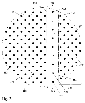
biochemical
reactions such that a different colored dye (for example, red, green, blue, or
yellow)
corresponds to each one. For example, a fluorescence microscope or other
suitable optical
system may be used to take images of the biochemical experiments disposed
and/or
conducted on an array chip. The colors observed indicate the DNA bases at that
particular
experiment step. Extracting data from an array chip with such DNA experiments
thus
depends on recording the color of fluorescence emitted by many millions or
even billions of
biochemical experiments that may be present on the chip.
[0008] However, obtaining useful data from a fluorescence image of a dense
biochemical
array chip is complicated by competing interests of spatial resolution,
accuracy, and speed.
Images must be obtained at high enough magnification for individual
experiments to be
clearly resolved. At the same time images must cover a large enough field of
view for
experiments to be correctly identified. Finally, for large scale studies,
imaging and image
processing must take place quickly enough to provide for sufficient throughput
and to make
sequencing operations commercially feasible.
SUMMARY
[0009] Described herein are principles for, and various embodiments of, high-
density array
chips that address the competing interests involved in imaging and image
processing of
biochemical experiments disposed on the chips. For example, the high-density
array chips
described herein address the problem of how to achieve a very high density of
biochemical
experiments on the chips while at the same time allowing for rapid extraction
of data from
images of the chips. Further, the high-density array chips described herein
also address the
problem of how to provide for real-time alignment between an array chip and an
imaging
instrument that is used to take the images of biochemical experiments disposed
on the chip
during operation. As illustrated in the various embodiments and principles
described herein,
these problems are addressed by encoding information on an array chip in the
foini of one or
2
CA 02809668 2013-02-26
WO 2012/031011 PCT/US2011/050047
more track regions that have different pitch and/or different density than
other regions of the
chip.
[0010] For example, the high-density array chips described herein provide for
track regions
that occupy a small percentage of the total area of the chips, while the rest
of the chips' area
is occupied by regions having a different and/or more dense array grid.
Information encoded
as one or more track regions of an array chip is used in operation to reduce
the time necessary
to align an imaging instrument (e.g., such as a fluorescence microscope
camera) with the
chip, while at the same time providing for real-time adjustment of such
alignment. The real-
time alignment of the imaging instrument is achieved by continuously
monitoring for
alignment errors based on information extracted from the images of the track
region(s) on the
array chip, and then correcting the alignment based on the alignment errors as
the imaging
instrument moves across the array chip and takes images of the biochemical
experiments
disposed thereon.
[0011] According to the principles and embodiments described herein, an array
chip
design, suitable for biochemical assays, is provided where the chip includes a
field region
arranged with attachment sites according to a first pitch and at least one
track region having a
one-dimensional spot pattern arranged according to a second pitch that is less
dense and is a
non-integer multiple of the first pitch so that so one-dimensional Moire
averaging can be
applied in the track region, thereby to attain alignment of the chip to the
optical
instrumentation with a higher density of attachment sites.
[0012] In an example embodiment, a chip for assays comprises: a substrate
comprising a
field region and a track region; experiment sites disposed in a first
patterned array in the field
region, the first patterned array being defined by a first pitch; and
alignment sites disposed in
a second patterned array in the track region, the second patterned array being
defined by a
second pitch along a single dimension. The second pitch differs from the first
pitch by a non-
integer multiple in order to permit Moire averaging-based alignment.
[0013] In one aspect of this embodiment, the field region has a density of one
object space
pixel per one experiment site. In another aspect, the field region has a
density of two object
space pixels per one experiment site, where the experiment sites in the field
region are
arranged in a checkerboard pattern. In yet another aspect, the field region
has a density of
four object space pixels per one experiment site.
[0014] In one aspect, the alignment sites in the track region are operative to
support
biochemical experiments. In another aspect, selected ones of the alignment
sites are deleted
3
CA 02809668 2013-02-26
WO 2012/031011 PCT/US2011/050047
in accordance with a preselected pattern. In yet another aspect, selected ones
of the
alignment sites are deleted in accordance with a pseudo-random pattern.
[0015] In one aspect, the experiment sites in the field region and the
alignment sites in the
track region are both configured to support biochemical experiments. In one
aspect, the
experiment sites in the field region and the alignment sites in the track
region are configured
to support attachment of DNA nanoballs.
[0016] In one aspect, the areas of the substrate of the array chip that are
different than the
experiment sites (in the field region) and the alignment sites (in the track
region) are
chemically treated to inhibit binding of target nucleic acids.
[0017] In one aspect the single dimension, along which the track region is
disposed, is a
horizontal dimension. In another aspect the single dimension is a vertical
dimension.
[0018] In one aspect, the track region is separated from the field region by a
site-free band.
In another aspect, the size of the track region is one of: three times the
size of an object space
pixel, and five times the size of an object space pixel.
[0019] In one aspect, the substrate of the array chip further comprises a
horizontal track
region that is disposed substantially perpendicular to the vertical track
region, where the
horizontal track region comprises track sites disposed according to the second
patterned array
along a second dimension that is substantially perpendicular to the single
dimension, along
which the track region is disposed.
[0020] In an example embodiment, a method comprises: an imaging instrument
taking an
image of a chip on which target nucleic acids have been disposed, where the
chip comprises:
a substrate comprising a field region and a track region, experiment sites
disposed in a first
patterned array that is defined by a first pitch and that is disposed in the
field region, and
alignment sites disposed in a second patterned array that is defined by a
second pitch along a
single dimension and that is disposed in the track region, where the second
pitch differs from
the first pitch by a non-integer multiple and the target nucleic acids are
attached to the
experiment sites and the alignment sites; a correlation logic determining a
correction
alignment tern' for the single dimension by using, at least in part, Moire
averaging based on
signals recorded in the image that are emitted from the target nucleic acids
attached to the
alignment sites in the track region; and automatically aligning the chip with
the imaging
instrument along the single dimension based on the correction alignment terni.
4
WO 2012/031011 CA 02809668 2013-02-26 PCT/US2011/050047
[0021] In one aspect of this embodiment, the substrate of the chip further
comprises a
horizontal track region that is disposed substantially perpendicular to the
vertical track
region, where the horizontal track region comprises track sites disposed
according to the
second patterned array along a second dimension that is substantially
perpendicular to the
single dimension. In this aspect, the method further comprises: the
correlation logic
determining a second correction alignment term for the second dimension by
using, at least in
part, Moire averaging based on signals recorded in the image that are emitted
from the target
nucleic acids attached to the track sites in the second track region; and
automatically aligning
the chip with the imaging instrument along the second dimension based on the
second
correction alignment term.
[0022] In one aspect of this embodiment, the step of the correlation logic
determining the
correction alignment term for the single dimension further comprises: as part
of the
correction alignment tem', determining a track pitch misalignment error based
at least in part
on: the signals recorded in the image that are emitted from the target nucleic
acids attached to
the alignment sites in the track region, and information representing a
pattern of deletion sites
in the at least one track region.
[0023] In one aspect, the target nucleic acids attached to the chip comprise
DNA nanoballs.
In another aspect, a subset of the alignment sites in the track region are
selectively deleted to
form a pattern of deletions, and step of the correlation logic determining the
correction
alignment term further comprises computing the correction alignment term based
at least in
part on an ordered data set that represents the pattern of deletions.
[0024] The invention can be better understood by reference to the following
detailed
description in connection with the accompanying drawings.
BRIEF DESCRIPTION OF THE DRAWINGS
[0025] Fig. 1 is a top plan view of a portion of a high-density biochemical
array chip with
an inset illustrating an example pattern for field regions and track regions
(size not to scale).
[0026] Fig. 2 is a top plan view with an inset of one field of an example high-
density
biochemical array chip showing details of a field region and one track region
(size not to
scale).
[0027] Fig. 3 is a top plan view of part of a subfield of one field region and
one track
region of an example high-density biochemical array chip illustrating one
embodiment of a
5
CA 02809668 2013-02-26
WO 2012/031011 PCT/US2011/050047
layout pattern of attachment sites relative to an overlay of pixels showing
relative scale and
position in accordance with the invention.
[0028] Fig. 4 is a top plan view of part of a subfield of one field region and
one track
region of an example high-density biochemical array chip illustrating another
embodiment of
a layout pattern of attachment sites relative to an overlay of object space
pixels showing
relative scale and position.
[0029] Fig. 5 is detail of a portion of Fig. 4 for illustrating that the
period of the field region
and the track region are non-integer multiples of one another.
[0030] Fig. 6 is a diagram for illustrating one-dimensional "Moire averaging"
techniques.
[0031] Fig. 7 is a diagram for illustrating offset determination using
deletion patterns.
DETAILED DESCRIPTION
[0032] In the following description, for the purposes of explanation, numerous
specific
details are set forth in order to provide a thorough understanding of the
present invention. It
will be apparent, however, to the skilled in the art, that the present
invention may be practiced
without all or some of these specific details.
Selected Definitions
[0033] "Array chip" (or simply "chip") refers to a solid phase support (e.g.,
such as a
substrate) having a surface, preferably but not exclusively a planar or
substantially planar
surface, that carries an array of sites to which nucleic acids or
macromolecules can attach to
form a biochemical assay. When attached to a site, the nucleic acids or
macromolecules may
be covalently bound to the solid support of the array chip, or may be non-
covalently bound.
Typically, the identities of the attached nucleic acids or macromolecules are
not discernable,
at least initially, from their site locations but may be determined by a
particular operation on
the array, such as by sequencing, hybridizing decoding probes, or the like.
See, e.g., US Pat.
Nos. 6,396,995; 6,544,732; 6,401,267; and 7,070,927; WO publications WO
2006/073504
and 2005/082098; and US Pub Nos. 2007/0207482 and 2007/0087362.
[0034] "Fluorophores" are any molecules comprising or consisting of a
functional group
that absorbs energy within a specific absorption spectrum and re-emits energy
(e.g., such as
light) at a different (but equally specific) emission spectrum. Preferred
fluorophores for use
as markers include, but are not limited to, fluorescein, cascade blue,
hexachloro-fluorescein,
tetrachloro-fluorescein, TAMRA, ROX, FAM, Cy3, Cy3.5, Cy5, Cy5.5, Texas Red,
Eosin,
6
CA 02809668 2013-02-26
WO 2012/031011 PCT/US2011/050047
the DyLight Fluor family available from Thermo Fisher Scientific of Waltham,
Massachusetts, and the Alexa Fluor family from Molecular Probes of Eugene,
Oregon.
[0035] "Image space" refers to the area covered by the set of pixels in a
camera, and
"image space pixel" refers to a camera pixel.
[0036] "Logic" refers to a set of instructions which, when executed by one or
more
processors, are operable to perform one or more functionalities and/or return
data in the form
of one or more results. In various embodiments and implementations, any such
logic may be
implemented as one or more software components that are executable by one or
more
processors, as one or more hardware components such as Application-Specific
Integrated
Circuits (ASICs) and/or Field-Programmable Gate Arrays (FPGAs), or as any
combination of
one or more software components and one or more hardware components. The
software
component(s) of any particular logic may be implemented, without limitation,
as a standalone
or client-server software application, as one or more software modules, as one
or more
libraries of functions, and as one or more static and/or dynamically-linked
libraries.
[0037] "Macromolecule" used in relation to a nucleic acid means a nucleic acid
having a
measurable three dimensional structure, including linear nucleic acid
molecules with
comprising secondary structures (e.g., amplicons), branched nucleic acid
molecules, and
multiple separate copies of individual sequences with interacting structural
elements, e.g.,
complementary sequences, palindromes, or other sequence inserts that cause
three-
dimensional structural elements in the nucleic acid.
[0038] "Nucleic acid", "oligonucleotide", "polynucleotide", "oligo" or
grammatical
equivalents used herein refers generally to at least two nucleotides
covalently linked together.
A nucleic acid generally will contain phosphodiester bonds, although in some
cases nucleic
acid analogs may be included that have alternative backbones such as
phosphoramidite,
phosphorodithioate, or methylphophoroamidite linkages; or peptide nucleic acid
backbones
and linkages. Other analog nucleic acids include those with bicyclic
structures including
locked nucleic acids, positive backbones, non-ionic backbones, and non-ribose
backbones.
Modifications of the ribose-phosphate backbone may be done to increase the
stability of the
molecules; for example, PNA:DNA hybrids can exhibit higher stability in some
environments.
[0039] "Object space" refers to the area of an object such as an array chip,
and thus "object
space pixel" refers to a unit of area on an object such as an array chip. The
size of object
space pixels is typically determined by the size of the image space pixels
(i.e., camera pixels)
7
WO 2012/031011 CA 02809668 2013-02-26PCT/US2011/050047
and the magnification that is applied when the camera is used to take images
of the object
space. The magnification is the ratio of the size of an image space pixel
(i.e., a camera pixel)
to the actual size of the object space area that corresponds to the image
space pixel as
observed by the camera. For example, a magnification of 16X allows a camera
using 8 p,m
pixels to observe 500 nm object space pixels. In various embodiments, the size
of an object
space pixel may be between 200-1000 nm in width and 200-1000 nm length; in a
preferred
aspect the size of an object space pixel may be 320 nm by 320 nm, more
preferably 600 nm
by 600 nm, even more preferably 500 nm by 500 nm. In some embodiments, the
size of an
object space pixel is selected to be substantially the same as, or slightly
bigger, than the size
of a site on an array chip, so that only a single discrete site will fit into
an object space pixel.
This ensures that, in operation, the intensity of the energy (e.g., light)
emitted from a site on
the array chip can be recorded by a single camera pixel.
[0040] "Pitch" (also referred to as "period") refers to a uniform distance
that defines a
pattern such as, for example, an array. The pitch of an array chip, or a
region thereof, refers
to the uniform distance between the centers of any two adjacent sites disposed
in an array
grid on the chip, thereby defining the array of the chip, or the region
thereof. The pitch of a
camera refers to the uniform distance between the centers of any two adjacent
camera pixels
and defines the pixel array of the camera.
[0041] "Sequence determination" in reference to a target nucleic acid means
determination
of information relating to the sequence of nucleotides in the target nucleic
acid. Such
information may include the identification or determination of partial as well
as full sequence
information of the target nucleic acid. The sequence information may be
determined with
varying degrees of statistical reliability or confidence. In one aspect, the
term includes the
determination of the identity and ordering of a plurality of contiguous
nucleotides in a target
nucleic acid starting from different nucleotides in the target nucleic acid.
[0042] "Site" (also referred to as "spot") refers to a spatially defined area
on an array chip
that does not overlap with other sites on the chip; that is, the sites on an
array chip are
spatially discrete and may be arranged in a particular pattern. On an array
chip, a site is
typically configured to have dimensions (e.g., length, width, and possibly
depth or height)
that are suitable for the attachment of nucleic acids or macromolecule(s).
Examples of sites
include, but are not limited to, depressions, raised areas, micro-wells,
beads, and the like.
[0043] "Target nucleic acid" means a nucleic acid (or a macromolecule thereof)
from a
gene, a regulatory element, genomic DNA (including, but not limited to, human
DNA),
8
CA 02809668 2013-02-26
WO 2012/031011 PCT/US2011/050047
cDNA, RNAs including mRNAs, rRNAs, siRNAs, miRNAs and the like, and fragments
thereof A target nucleic acid may be a nucleic acid from a sample, or a
secondary nucleic
acid such as a product of an amplification reaction.
Array Chip Imaging
[0044] Image-based techniques identify individual biochemical experiments on
an array
chip by the positions of the sites on which the experiments are disposed on
the chip. For
example, the intensity of the energy (e.g., such as light) emitted from the
sites is recorded as
an image, and the image is then processed to determine the positions of the
sites on the chip.
A biochemical experiment may be identified by the coordinates of its site on
the chip in a
two-dimensional (e.g., X-Y), planar coordinate system, for instance. An image
of an array
chip typically includes a large enough area such that locations of the
experiments' sites may
be measured and/or computed with respect to the coordinate system in use. Some
prior
approaches use conventional alignment marks (e.g., such as cross etchings) for
this purpose;
however, drawbacks of such marks include difficulty of observing them with
fluorescence
microscopes, incompatibility of materials, and wasted chip area. In contrast,
the high-density
array chips described herein use the biochemical experiments themselves
(arranged in
specific patterns), and the energy emitted therefrom, to aid identification.
[0045] In various operational contexts, images of the biochemical experiments
disposed on
an array chip may be obtained with an imaging instrument that includes a
camera attached to
a fluorescence microscope. The magnification of the microscope determines how
many
biochemical experiment sites can be "seen" by a camera pixel at the one time;
equivalently,
the magnification determines the ratio of the size of a camera pixel (in image
space) to the
size of a chip area (in object space) that is observed and corresponds to the
camera pixel. For
example, a magnification of 16X allows a camera using 8 pm pixels to record
signals from
500 nm chip areas (e.g., object space pixels). Thus, the rate at which data
may be extracted
from an array chip depends, in part, on how many camera pixels correspond to
each spot on
the chip (presuming that the size of a spot is smaller than the size of an
object space pixel).
For example, a one-megapixel camera operating at twenty camera pixels per spot
can image
50,000 spots. If the same camera is operated with two (or even one) camera
pixel per spot,
the number of spots per image is ten (or twenty) times greater. While low
pixel-to-spot ratios
(e.g., such as 1:1, 2:1, and 4:1) are very desirable since they greatly
increase imaging
throughput, they also impose very demanding requirements on the alignment of
the camera
pixels with the array chip spots during operation.
9
CA 02809668 2013-02-26
WO 2012/031011 PCT/US2011/050047
[0046] According to the principles and embodiments described herein, carefully
designed
spatial patterns of sites for biochemical experiments on an array chip aid the
accuracy and
speed of data acquisition via fluorescence imaging. The specific layout
principles described
hereinafter enable rapid imaging of very high density biochemical arrays and
thus improve
the throughput of large scale imaging systems such as genome sequencing
systems. Further,
the described novel chip designs aid accuracy of chip alignment and
identification while
maximizing the area of the chip that can be used for biochemical experiment
sites.
[0047] As described herein, precise alignment correcting for fractional
offsets is achieved
by correcting for errors in sub-pixel X-Y alignment by use of Moire averaging.
In Moire
averaging, magnification is intentionally set so that the period of the object
space pixels
corresponding to the pixels of the imaging element (e.g., a camera) is a non-
integer multiple
of the period that defines the sites in a track region of the chip. Accurate
pixel-level
alignment is achieved by providing for pre-defined and pseudo-randomly
disposed sets of
sites (herein referred to as deletion or reserved sites), on which biochemical
materials are
prevented from attachment to the chip substrate so that the deletion sites of
the array can be
used in a pattern matching scheme as registration markers for absolute
location identification.
Additional techniques for initial registration and subsequent correction of
scale, rotation, and
X-Y offsets for high-density array chips are described in: (1) U.S. Patent
Application Serial
No. 13/092,618, filed on April 22, 2011 and entitled "METHOD AND SYSTEM FOR
ACCURATE REGISTRATION OF ARRAY FOR DNA SEQUENCING", the entire
contents of which is hereby incorporated by reference for all purposes as if
fully set forth
herein; and (2) U.S. Patent Application Serial No. 12/912,641, filed on
October 26, 2010 and
entitled "METHOD AND SYSTEM FOR IMAGING HIGH DENSITY BIOCHEMICAL
ARRAYS WITH SUB-PIXEL ALIGNMENT", the entire contents of which is hereby
incorporated by reference for all purposes as if fully set forth herein.
High-Density Array Chips with Track Regions
[0048] Turning now to Fig. 1, a high-density biochemical array chip according
to one
embodiment is shown. Chip 100 is based on a solid, planar substrate and is
conveniently
dimensioned in several centimeters in length and width. Typical chip
dimensions may be 2.5
cm by 7.5 cm by 0.1 cm, for example. Smaller chips (e.g. less than about 0.5
cm on a side)
are possible but may be less convenient to handle in some operational
contexts, and it may be
difficult to maintain required flatness for larger chips (e.g., more than
about 10 cm on a side).
In some embodiments, chips designed according to the principles described
herein may
support more than one billion biochemical exneriments. For example, in cPAL
sequencing
10
CA 02809668 2013-02-26
WO 2012/031011 PCT/US2011/050047
with DNA nanoballs (which is described in a separate section hereafter), each
experiment is
carried out within a circular area approximately 300 nm in diameter. In other
embodiments,
biochemical experiments may be carried out on chip sites that are between 30-
1000 nm in
diameter (or length and width), or even 200-500 nm in diameter (or length and
width).
[0049] To break the imaging problem into manageable chunks, array chips are
divided into
micron-to-millimeter sized fields; e.g. field 105. In one embodiment, a
typical field may be
500 pm by 500 iim; thus a typical chip is divided into hundreds or thousands
of fields. In
other embodiments, a field may be of sizes that are between 320-1600 pm by 320-
1600 um,
600 pm by 600 um, or even 1.6 mm by 700 um.
[0050] Fig. 2 is a diagram of one field 205 of a high-density biochemical
array chip. The
field is divided into subfields (e.g. 210, 212, 214) separated by track
regions that are aligned
substantially along a horizontal X dimension (e.g. track region 220) and by
track regions that
are aligned substantially perpendicular to the X dimension regions along a
vertical Y
dimension (e.g., track regions 224, 226). A magnified view 230 shows spots in
two subfields
separated by track region 226. The chips of Figs. 1 and 2 do not include any
marks or
features used for alignment other than track regions that separate the
subfields. Properties of
the track regions, principles by which they are laid out, and their
relationship to the subfields
are discussed in detail below.
[0051] Fig. 3 is a diagram of part of a subfield of one field of a high-
density biochemical
array chip according to an example embodiment. The circular area 330
represents the same
magnified view of a field as view 230 in Fig. 2. In this view, for
illustration purposes only,
track region 326 is bounded by heavy dashed lines 380 and 381; in practice
however, such
dashed lines are not present on the array chip itself.
[0052] In the embodiment illustrated in Fig. 3, the width of vertical track
region 326 is set
to equal the length of 3 object space pixels, which correspond to camera (or
image space)
pixels according to the applicable magnification. In this embodiment, the
height of a
horizontal track region may be the same as the width of track region 326. In
some
embodiments, the width of a vertical track region (and similarly, the height
of a horizontal
track region) may be equal to 5 object space pixels in the array grid of the
adjacent non-track
regions. As illustrated in Fig. 3, a site-free band separates track region 326
from each of the
adjacent regions 340 and 345. In operation, these site-free bands prevent the
light signals,
emitted from the experiments disposed on the more densely populated regions
340 and 345,
from interfering with the signals emitted from the experiments disposed on the
sites of track
11
CA 02809668 2013-02-26
WO 2012/031011 PCT/US2011/050047
region 326. In other embodiments, the track region does not need to be
separated from the
field regions with site-free bands; rather, in these embodiments a correlator
logic may be used
to correctly process the signals recorded in an image of the track region even
if the track
region is embedded into a field region without a separation site-free band.
For example, the
correlator logic may be configured to distinguish between the "on-pitch"
signals from the
field region and the different, "off-pitch" signals of the track region by
relying on the
property that "on-pitch" signals tend to get easily canceled out by averaging
to zero.
[0053] In the embodiment of Fig. 3, regions 340 and 345 are parts of adjacent
subfields on
either side of track region 326. Fluorescent spots (e.g. 351, 352, and 353)
appear in the
subfields; fluorescent spots (e.g. 360, 362) are also seen in the track region
326. In this
embodiment, there is no difference in the biochemical experiments disposed on
subfield spots
and track region spots, or in the fluorescent markers that are used to tag the
experiments.
Open circles (e.g. 361) represent the intentional absence of a spot, e.g., a
deletion spot. Such
deletion spots are conveniently made by deleting corresponding features on a
photolithography mask used to pattern the sites on an array chip. According to
the principles
described herein, the deletion spots preferably account for more than 5% of
the available spot
locations in the track region but less than 15%. The spots in the track region
may be
attachment sites for biochemical or fluorescent molecules, the same or similar
to sites in the
field region. The deletion spots may be the absence of attachment sites, or
they may be
attachment sites that have been subsequently chemically treated to inhibit or
prevent binding
with biochemical or fluorescent molecules.
[0054] For illustration purposes only, light dashed lines (e.g. 370, 371) in
Fig. 3 indicate
the boundaries between the object space pixels that correspond to the
boundaries of the
physical pixels (e.g., the image space pixels) in a camera that is used to
image the chip at a
specific magnification. Thus, while Fig. 3 is drawn at a resolution much finer
than a
camera's pixel period, an image of region 330 taken with a camera having
pixels bounded by
the light dashed lines in the figure could not resolve spatial features finer
than the pixel
period. Despite this limitation, the layout of spots in the track region
permits alignment of
spots to pixels with sub-pixel resolution as described below.
[0055] The layout of spots on the chip shown in Fig. 3 (and therefore the
layout of the
biochemical experiments on the chip in operation) provides for a two-to-one
ratio of object
space pixels to array spots in regions 340 and 345 that are part of subfields
on the array chip.
That is, the area in regions 340 and 345 is configured at a density of two
object space pixels
per one array spot. To the extent that track regions take up only a few
percent of the total area
12
WO 2012/031011 CA 02809668 2013-02-26 PCT/US2011/050047
of a field, the two-to-one pixel to spot ratio holds approximately for an
entire chip. Higher
density layouts are possible, however, as further described below.
[0056] For example, Fig. 3 illustrates an array chip in which the spots in the
subfield
regions are disposed on an array in a checkerboard pattern. An array with a
checkerboard
pattern has a spot pitch of:
4-2 * the array pitch,
and it is the diagonal distance between the centers of any two adjacent spots.
For example,
for an array with an object space pitch of 500 nm, the spot pitch defining a
checkerboard
pattern would be:
* 500 = 707 nm.
Viewed in another way, in an array with spots arranged in a checkerboard
pattern, the spots in
each adjacent row are offset by +1 column.
[0057] In fluorescent imaging, using a checkerboard pattern on an array chip
helps because
light from a chip spot may typically bleed horizontally or vertically across
to adjacent spots
but not to corner spots. Thus, disposing the spots of an array chip in a
checkerboard pattern
allows for the very high density of two object space pixels (and, therefore
two camera pixels)
per one spot while at the same time minimizing the crosstalk from signal
bleeding within the
electronics of the imaging instrument.
[0058] Fig. 4 is a diagram of part of a subfield of one field of a high-
density biochemical
array chip according to an example embodiment. Fig. 4 is similar to Fig. 3
except that in Fig.
4, the object space pixel (and, therefore, the camera pixel) to array spot
ratio is one-to-one in
the subfields. Circular area 430 represents the same magnified view of a field
as view 230 in
Fig. 2 and view 330 in Fig. 3. In this view, for illustration purposes only,
track region 426 is
bounded by heavy dashed lines; in practice however, such dashed lines are not
present on the
array chip itself.
[0059] In the embodiment illustrated in Fig. 4, the width of vertical track
region 426 is set
to equal the length of 3 array (or object space) pixels, which correspond to
camera (or image
space) pixels according to the applied magnification. In this embodiment, the
height of a
horizontal track region on the array chip may be the same as the width of
track region 426. In
other embodiments, the width of a vertical track region (and similarly, the
height of a
horizontal track region) may be equal to 5 object space pixels in the array
grid of the adjacent
13
CA 02809668 2013-02-26
WO 2012/031011 PCT/US2011/050047
non-track regions. As illustrated in Fig. 4, a site-free band separates track
region 426 from
each of the adjacent regions 440 and 445. In operation, these site-free bands
prevent the light
signals, emitted from the experiments disposed on the more densely populated
regions 440
and 445, from interfering with the signals emitted from the experiments
disposed on the sites
of track region 326. In other embodiments, the track region does not need to
be separated
from the field regions with site-free bands; rather, in these embodiments a
correlator logic
may be used to correctly process the signals recorded in an image of the track
region even if
the track region is embedded into a field region without a separation site-
free band. For
example, the correlator logic may be configured to distinguish between the "on-
pitch" signals
from the field region and the different, "off-pitch" signals of the track
region by relying on
the property that "on-pitch" signals tend to get easily canceled out by
averaging to zero.
[0060] Regions 440 and 445 are parts of adjacent subfields on either side of
track region
426. Fluorescent spots (shown as black dots) appear in the subfields and in
the track region.
There is no difference in the biochemical experiments represented by subfield
spots and track
spots, or the fluorescent markers used to see them. Open circles (e.g. 461)
represent the
intentional absence of a spot (e.g., a deletion spot). Such deletion spots may
be conveniently
made by deleting corresponding features on a photolithography mask used to
pattern the sites
on an array chip.
[0061] The layout of spots shown in Fig. 4 (and therefore the layout of the
biochemical
experiments on the chip in operation) provides for a one-to-one ratio of
object space pixels to
array spots in regions 440 and 445 that are part of subfields on the array
chip. That is, the
area in regions 440 and 445 is configured at a density of one object space
pixel (and,
therefore, one camera pixel) per one array spot. This layout leads to a very
large amount of
information contained in each field image. For example, in the embodiment
illustrated in Fig.
4, approximately 5% of the chip area is used for track regions and the
remaining 95% percent
of the chip area is used at maximum density of one object space pixel (and,
therefore, one
camera pixel) per one array spot.
[0062] In other embodiments according to the principles described herein, the
sites in the
non-track regions of an array chip may be disposed in a layout that provides a
density of 4
object space pixels (and, therefore, 4 camera pixels) per one site. Even
though such 4:1
pixels-per-site density is lower than the site densities illustrated in Fig. 3
and Fig. 4, it is still
a very high density when compared with the densities of conventional array
chips; at the time
of filing of the present application, commercially available biochemical array
chips have
densities in the range of 10:1 to 25:1 pixels-Der-site density.
14
CA 02809668 2013-02-26
WO 2012/031011
PCT/US2011/050047
[0063] The design of the high-density array chips described herein leaves
little room for
imaging error because misalignment of camera pixels and array spots of as
little as one
quarter (0.25) pixel period can lead to unacceptable data acquisition errors.
To address this,
described below are techniques for designing array chips with track regions
that provide for
alignment within a desired tolerance, as well as techniques for using Moire
averaging in
correcting alignment errors.
Determination of the Parameters for the Track Region Structure
[0064] According to the principles and embodiments described herein, the
layout of the
sites in a track region (also referred to as "track sites") is determined in
accordance with the
desired tolerance for aligning the camera pixels with the sites on the array
chip. To
determine how many track sites are necessary to achieve a particular sub-pixel
alignment
tolerance (and therefore the pitch of the track region), the following
calculations may be used.
[0065] As an example, suppose that an alignment tolerance measurement error of
5 nm is
desired for a perfectly pre-aligned system and Moire averaging is to be used
for aligning the
camera pixels with the sites on an array chip. The measurement error of any
site in the track
to the array may be as large as 0.5 pixels, and thus the averaged error for
an individual
object space pixel i is approximately 0.25 pixels, e.g.,
errorki I 0.25 the size of an object space pixels.
For the purposes of Moire averaging, the averaged alignment error is the
difference between
the average of the sum of all alignment errors and the correct alignment
value, that is
N
_E err or ¨ correctõ uõ *¨ * the size
of an object space pixel (1)
where N is the number of measurements (e.g., number of track sites emitting
signals) and
"correct value" is the actual (but unknown) alignment error. For example, if
the desired
accuracy is 1740th of an object space pixel, then the desired N is about 100.
[0066] In an array chip with 8 track regions each having 8 sub-regions that
each has 59
track sites, there are a total of
8* 8 * 59 = 3776
track sites. Since in DNA sequencing a target nucleic acid will generate a
signal a quarter of
the time on average (e.g., a target nucleic acid will produce a signal for
either A, T, C, or G),
only about quarter of the track sites can be expected to emit a signal. That
is, it can be15
CA 02809668 2013-02-26
WO 2012/031011
PCT/US2011/050047
expected that approximately 944 sites (e.g., 3776/4)will emit a signal during
operation.
According to equation (1) above, with N = 944 the theoretical averaged
alignment error can
be expressed as
1
the size of an object space pixel
4 44
Thus, for an object space pixel of 500 nm, the theoretical averaged alignment
error is
1
* 500 4.O7 nm
V944
Practical observations for array chips with 500 nm object space pixels have
confirmed that
the practical measured error for 59 track sites per track sub-region is about
5 nm, which is
close to the theoretical value.
[0068] The above calculations indicate that a certain number of track sites
arranged in a
track region along a single dimension (e.g., such as a horizontal X dimension
or a vertical Y
dimension) allow for using Moire averaging to calculate the X-Y alignment
errors and to
align the camera pixels with the array chip sites to within a desired
tolerance. (It is noted that
in one embodiment, a tolerance of 5 nm is sufficient for taking accurate
signal intensity
measurements in DNA sequencing.) In addition, the above calculations indicate
that a very
low alignment tolerance (e.g., such as 5 nm) can be achieved by losing only
about 5% of the
array chip area to track regions, which is very useful in implementations
(such as high
throughout DNA sequencing) where high density of array spots is necessary for
efficient
operation.
Alignment Correction by Using Moire Averaging
[0067] The track regions of the high-density array chips described herein
(e.g., as
illustrated in Fig. 3 and Fig. 4) are designed such that an imaging system can
use them for
several simultaneous operations: (1) alignment of fields with sub-pixel
precision; and (2)
absolute location of spots in a pixel coordinate system. Principles underlying
the first of
these operations, alignment of fields with sub-pixel precision, are discussed
in connection
with Figs. 5 and 6.
[0068] Fig. 5 is a diagram illustrating relationships between periods of
subfield spots and
alignment track spots in a high-density biochemical array chip. Fig. 5 shows a
small section
of a subfield 505 and an adjacent track 510 in a field of a chip having a two-
to-one camera
pixel to array spot ratio in which the spots are arranged in a checkerboard
pattern. (The entire
16
CA 02809668 2013-02-26
WO 2012/031011 PCT/US2011/050047
discussion of Fig. 5 would be unchanged, however, if the pixel to spot ratio
were one-to-one.)
Light dashed lines (e.g. 515, 520) show the boundaries between object space
pixels that
correspond to the boundaries of the physical pixels (e.g., the image space
pixels) in a camera
that is used to image the chip at a specific magnification, while heavy dashed
line 530 marks
the boundary between subfield region 505 and track region 510. (It is noted
that the light
dashed lines 515, 520 and the heavy dashed lines 530 are included in Fig. 5
for illustration
purposes only; in practice, such dashed lines are not present on the array
chip itself.)
[0069] Field spots (e.g. 540, 541, and 542) in subfield 505 are repeated in
the X and Y
dimensions with a period 4, where XF is the period for field spots. Track
spots (e.g. 550,
551, and 552) in track region 510 are repeated in the Y dimension with a
period XT, where XT
is the period for spots in the track region. (Deleted spots, drawn as open
circles (e.g. 560),
are included when measuring the track spot repetition period.) By the design
of the array
chip, there is an intentional, non-integer-multiple mismatch between X.F and
kr; i.e. kr n XF
where n is an integer. The mismatch may be easily seen in Fig. 5 as some track
spots lie near
the middle of an object space pixel (e.g. track spot 552) while others lie
near pixel boundaries
(e.g. track spot 550).
[0070] When the period of field spots is the same as, or an integer multiple
of, the object
space pixel period that corresponds (under the applied magnification) to the
pixel period in a
camera used to image a chip, the careful choice of a non-integer-multiple
ratio between the
period of field spots and the period of track spots increases the ability to
accurately align a
camera with the spots on the chip during operation. The increased accuracy is
obtained
because the diversity of track spot locations within the object space pixels
may be averaged
to calculate an average track spot position. If the track spots' period were
the same as that of
JP
the camera pixels, errors of as much as V2 (where 4, the object space pixel
period, is
equal to or an integer sub-multiple of )F) could result. This one-dimensional
Moire averaging
alignment technique is illustrated in Fig. 6.
[0071] A track spot period, XT, that is not an integer multiple of the object
space pixel
period, 4, is shown in a conceptual, one-dimensional example of imaging track
spots in Fig.
6. In Fig. 6, a line of track spots including spots 600, 605, etc., has a
period or pitch between
spots, of XT. A line of object space pixels (which, subject to the applied
magnification,
correspond 1:1 with camera pixels), including pixels 620, 625, 630, etc., has
a period of kp.
For illustration purposes, in the example of Fig. 6, 8XT = 94 (equivalently,
kr = 1.125Xp).
17
CA 02809668 2013-02-26
WO 2012/031011 PCT/US2011/050047
When the track spots are observed with the line of pixels (as shown at 640
where the pixels
are labeled "1" through "9"), the track spot and object pixel are aligned
every ninth pixel.
The relative positions of the track spots and pixels sweep through each other
in the
intervening pixels. Inset 650 is a magnified view of object space pixels "1"
through "9"
superposed upon each other. The track spots are spread evenly across the
superposed pixel.
The difference in track spot pitch and pixel period leads to the track spots
sampling the length
of the pixel in equal steps. The average of all the track spot locations in
superposition 650
leads to an estimate of the best fit track spot location in pixel coordinates
with an error that is
reduced by a factor of al where N is the number of pixels between repeats; N =
9 in this
example. In practice, in one embodiment an array chip is configured with N =
59 track spots
that are evenly spread over 125 object space pixels, thereby yielding a track
spot pitch of kr =
125
Xp, or kr = 2.1194. In another embodiment, an array chip is configured with N
= 67
track spots that are evenly spread over 125 object space pixels, thereby
yielding a track spot
125
pitch of XT = 67 4), or XT = 1.866X.
[0072] Thus, the location of the track spots may be determined with sub-pixel
precision
using Moire averaging, as described below.
[0073] The operation for determining the absolute location of spots in a pixel
coordinate
system can be performed based on the infoimation encoded in the layout of
spots in the track
region as follows. If the position of the track spots is known, the position
of field spots may
be calculated based on the known layout of subfield and track spots on a chip.
The position
of track spots may still be subject to offset errors of integer numbers of
track spot periods,
however. That is, during operation the camera pixels may be aligned with the
object space
pixels with sub-pixel precision, as described above, but there may still be
misalignment by
one or more pixels such that a particular camera pixel is aligned with the
wrong object space
pixel. Such "modulo one" track spot pitch ambiguities may be resolved through
the use of
deleted track spots, such as deleted spot 560 in Fig. 5.
[0074] The absolute location of track spots (and therefore field spots that
are fixed relative
to the track spots when the array chip is manufactured) may be determined by
analysis of
track spot deletion patterns as illustrated in Fig. 7. In Fig. 7, track 705
has both regular
illuminated spots (e.g. 706) and deleted spots (e.g. 707), corresponding to
active and deleted
attachment sites, respectively, on a chip. For illustration purposes, masks
710, 715 and 720
are shown as aids to conceptualization of cross correlating a known deletion
pattern with an
18
CA 02809668 2013-02-26
WO 2012/031011
PCT/US2011/050047
image of track spots. Masks 710 and 715 are misaligned (by plus or minus one
spot) while
mask 720 is aligned with the deletion pattern. When misaligned mask 710 or 715
is
superposed with track 705, light is transmitted through transparent openings
such as 712. On
the other hand, when mask 720 (which is correctly aligned with the deletion
pattern of track
705) is superposed with track 705, very little light passes through its
transparent openings as
they line up with deleted spot locations. Graph 725 shows transmitted light
versus offset
during cross correlation of a mask pattern with an image of a track encoded
with a deletion
pattern. The intensity of transmitted light drops sharply when the mask and
track are at the
proper offset with respect to one another. This correlation property of masks
with deleted
spots is used in practice by a correlation logic that is configured to take as
input an ordered
data set representing the intensities recorded from the track spots and an
ordered data set
representing the mask of deleted spots (which is known and fixed relative to
the object-space
pixel coordinate system), and to generate as output an alignment error term
that specifies the
offset of the track spots (in whole pixels) from their correct location in the
pixel coordinate
system.
[0075] If the deletion pattern for a track region is pseudo random, then the
pattern has a
wide spatial range; e.g., only one peak will appear in a cross correlation of
the pattern and an
image of the track region. If the deletion pattern is periodic, or partly so,
more than one peak
may appear in a cross correlation. Thus, pseudo-random deletion patterns are
robust when
the position of a track region must be identified with no a priori
information. On the other
hand, initial rough alignment may be good enough that deletion patterns are
not required to
be strictly pseudo random.
Example Method of Using Moire Averaging for Alignment Correction
100761 In operation, when target nucleic acids are disposed on an array chip,
Moire
averaging can be used to calculate the correction alignment term and to apply
this term
during the process of initial chip registration (e.g., when the chip is
affixed in a sequencing
machine stage prior to imaging) and during the process of continuously taking
images of the
chip (e.g., in a feed control that continuously corrects the alignment of the
imaging
instrument during imaging). The correction alignment term, ET for a single
dimension (such
as an X dimension or a Y dimension), is expressed as follows
ET = * ed 61;9 (2)
19
CA 02809668 2013-02-26
WO 2012/031011 PCT/US2011/050047
where ET is the correction alignment term for the specific single dimension,
XT is the pitch of
sites in the track region along the single dimension, ed is the track pitch
(whole-pixel)
misalignment error that is an integer value indicating whole pixels, and 6gv
is the sub-pixel
error determined by using Moire averaging. The size of the sub-pixel error,
es'P , is less than
the size (length or width) of an object space pixel as expressed by the
following inequality:
AT AT
¨ < e < ¨
2 sP 2
where kr is the pitch of sites in the track region along a single dimension
(e.g., the X
dimension or the Y dimension). Since in practice correction alignment may be
needed both in
the X dimension and the Y dimension, a first correction alignment term is
computed for the X
dimension based on information from a horizontal track region on the chip, and
a second
correction alignment term is computed for the Y dimension based on information
from a
vertical track region on the chip. The two correction alignment terms are then
both applied in
order to achieve the desired alignment between the camera pixels and the spots
on the array
chip.
[0077] In an example embodiment, a method for aligning an array chip comprises
several
steps. In the first step, an image of the sites in a track region (on which
target nucleic acids
have been disposed) is taken, and the signal intensities recorded in the image
are converted
into an ordered data set. For example, the camera in an imaging instrument may
snap one or
more images of a track region disposed along a single dimension, and an image
processing
logic may generate an ordered data set (referred to herein as "track site data
set") that
represents (e.g., as a linear profile) the intensities and positions of
signals emitted from the
track sites.
[0078] In the next step, the track site data set is correlated to an ordered
data set (referred to
herein as "expected data set") representing (e.g., as a linear profile) the
known/expected
positions of track sites that are defined by the site pitch of the track
region. Using Moire
averaging, the correlation returns the sub-pixel error for the particular
dimension along which
the track region is disposed. For example, a correlation logic may obtain the
sub-pixel error
based on multiplying the track site data set and the expected data set. In
another example,
correlation logic takes as input the track site data set and the expected data
set, and then
associates (discretizes) each signal recorded in the track site data set to
one discrete member
of the track site data set. To perform Moire averaging, the correlation logic
shifts the
expected data set with respect to the track site data set by I track pitch
(¨ 2 pixels) object
20
CA 02809668 2013-02-26
WO 2012/031011 PCT/US2011/050047
space pixels in sub-pixel increments. For each shift, the correlation logic
computes: (a) the
X2 error for each member of the track site data set representing a recorded
signal based on
the distance of that member to the closest member in the expected data set
that represents an
expected track site; and (b) the sum of the squares of all the X 2 errors
computed for that shift.
The correlation logic then determines the sub-pixel error based on the
smallest computed
squared-error sum from all shifts. This type of Moire averaging determines the
sub-pixel
error for the entire track region along the single dimension and, therefore,
also determines the
sub-pixel error for the field regions of the chip, which are fixed relative to
the track region
when the chip is manufactured. The Moire averaging mechanism effectively
averages the
error terms, err Or, of all track sites that have emitted a signal without
actually knowing or
determining the exact offset of each individual track site from the center of
some object space
pixel. The operations in this step may be performed separately for the X
dimension (on a
track site data set representing a track region in the horizontal X dimension)
and for the Y
dimension (on a track site data set representing a track region in the
vertical Y dimension) to
determine the sub-pixel error for the X dimension and the sub-pixel error for
the Y
dimension, respectively.
[0079] In the next step, the track site data set is correlated to ordered data
sets representing
(e.g., as linear profiles) one or more patterns of deletion spots in the track
regions (referred
herein as the deletion data sets). The correlation returns the track pitch
misalignment error
for the particular dimension along which the track region is disposed. For
example, a
correlation logic may take as input the track site data set and the deletion
data sets. The
correlation logic then compares the track site data set and the deletion data
sets to determine
that one deletion data set which most closely matches to the track site data
set. The
correlation logic then computes the track pitch misalignment error as the
offset, in whole
pixels, between the track site data set and the matching deletion data set.
The operations in
this step may be performed separately for the X dimension (on a track site
data set
representing a track region in the horizontal X dimension) and for the Y
dimension (on a
track site data set representing a track region in the vertical Y dimension)
to determine the
track pitch alignment error for the X dimension and the track pitch alignment
error for the Y
dimension, respectively.
[0080] In the next step, equation (2) above is used to determine the
correction alignment
term for the dimension along which the track region is disposed based on the
pitch of the sites
in the track region (which is known), the sub-pixel error computed for the
track region, and
the track pitch alignment error computed for the track region. For example, a
correction logic
21
CA 02809668 2013-02-26
WO 2012/031011 PCT/US2011/050047
may use equation (2) and the computed sub-pixel error and track pitch
alignment error to
calculate the correction alignment telin for the track region. The operations
in this step may
be performed separately for the X dimension (for a track region along the
horizontal X
dimension) and for the Y dimension (for a track region along the vertical Y
dimension) to
determine correction alignment telin for the X dimension and the correction
alignment term
for the Y dimension, respectively.
[0081] In the final step, the camera pixels and the array grid of the array
chip may be
aligned by the amount of the correction alignment terms for the X dimension
and the Y
dimension. For example, a lateral offset system in the imaging instrument may
adjust a galvo
to shift the position of images in the camera based on the correction
alignment term for the X
dimension. A time-delay integration (TDI) offset system in the imaging
instrument may
adjust the pulse timing of the camera based on the correction alignment term
for the Y
dimension. In this manner, the camera pixels and the array grid of the chip
may be aligned
with each other within the tolerance for which the layout of the track regions
in the chip has
been designed as described heretofore.
[0082] The principles of designing the layout of track sites and the Moire
averaging-based
alignment described herein may be used in various methods at various stages in
the
examination of biochemical experiments disposed on an array chip. For example,
in some
embodiments, the Moire averaging alignment based on track region information
as described
herein may be used to align an array chip during the process of initial chip
registration when
the chip is affixed in a sequencing machine stage prior to imaging.
[0083] In other embodiments, the Moire averaging alignment based on track
region
information as described herein may be used in a feed-forward control loop
during the
process of continuously taking images of the chip, where the alignment of the
imaging
instrument is corrected after taking each scan of the chip. For example, since
scanning two
adjacent columns of a chip results in negligible error offsets (e.g., 10-20 nm
or less), the X
and Y correction alignment terms can be accumulated across scans without
losing significant
alignment accuracy. Thus, after scanning a column and calculating its X and Y
correction
alignment terms, a feed-forward logic may add these two terms to the
corresponding
correction alignment terms that have been accumulated for the previously-
scanned columns.
In this manner, the correction alignment tern's for the X and Y dimensions for
a currently
scanned chip column are used to adjust the imaging instrument before the next
chip column is
scanned, thereby achieving a feed-forward alignment.
22
CA 02809668 2013-02-26
WO 2012/031011 PCT/US2011/050047
[0084] In summary, the layout of a high-density biochemical array chip affects
the rate of
biochemical experimental data that may be extracted from the chip. A high
density of
experiments may be achieved by matching the imaged repetition period of
experiments to the
pixel period (or a small integer multiple of the pixel period) of a camera.
Data acquisition
speed depends on alignment, absolute location, and identification of features
in experimental
images obtained, for example, by fluorescence microscopy. A chip layout with
asynchronous
tracks enables alignment within a desired tolerance. Moire averaging may be
used with
asynchronous tracks to determine sub-pixel alignment, while track deletion
patterns facilitate
resolution of modulo one errors that may be used for precise track pitch
alignment. For the
purposes of Moire averaging, the correction alignment terms in the X and Y
dimensions are
obtained from information reflecting a deliberately misalignment, during
manufacture,
between the sites in a track region with the grid on which the sites in a
regular field region lie.
A prime number (e.g., such as 59 or 67) is used to define such deliberate
misalignment
determine the alignment in order to achieve the necessary accuracy within a
desired
tolerance.
[0085] In an operational context of DNA sequencing, an example embodiment of
an array
chip with track regions as described herein allows a sequencing machine to
extract the
location of a snapped image with respect to the array chip at least as fast as
the machine is
taking the images. For example, in a sequencing machine comprising two cameras
that are
taking images of an array chip at a rate of 30 frames per second (fps) each,
1000 images
come through the machine every 15 seconds. By using array chips with track
regions as
described herein, the sequencing machine (or a component thereof) can
determine the X-Y
location of each image with respect to the chip within 15 milliseconds or
less. Specifically,
by using array chips with track regions as described herein, in one
implementation a
sequencing machine was able to determine the X-Y location of images at a rate
of 10
milliseconds with an accuracy of 5 nm.
Array Chip Construction
[0086] In some embodiments, array chips are constructed by disposing one or
more
layers (e.g., such as a reflective layer and/or a fluorescence enhancement
layer) on a
substrate. For example, the substrate of an array chip may itself be composed
of a reflective
material (e.g., such as a metal or a Bragg reflector), or it may be a base of
substantially any
coatable material that provides a solid support on which a fluorescent
reflective layer can be
disposed. The fluorescent reflective layer of the substrate may be made up of
a thin,
transparent, dielectric layer or a stack of thin, transparent, dielectric
layers, where such
23
CA 02809668 2013-02-26
WO 2012/031011 PCT/US2011/050047
dielectric materials include, but are not limited to, Si02, Ti02, Ta205, Hf02,
Zr02, MgO,
Si3N4, MgF2 and YF3.
[0087] In some embodiments, the sites on an array chip (e.g., such as sites in
track
regions and sites in field regions) may be defined by depressions or raised
areas in the
fluorescence reflective layer of the chip substrate. In such embodiments, the
array chip sites
may be between 30-1000nm in width and/or length, and in a preferred aspect the
sites may be
200-500nm in width and/or length, even more preferably approximately 300nm in
width
and/or length. In another specific aspect, the array chip sites may be
separated by a distance
of between 0.2pm and 10p,m. Target nucleic acids (e.g., such as nucleic acid
macromolecules) can be placed on the array chip sites to form an assay. The
target nucleic
acids are ideally disposed within each discrete site in a manner that provides
very high
density and discrete analysis of the individual nucleic acid constructs
contained therein. In
specific aspects, each site of an array chip is configured to accept a single
macromolecule
and, when macromolecules are disposed on the chip, a single macromolecule
attaches in each
site. In some embodiments the distance between the target nucleic acid
molecules, which
have attached to the sites on an array chip, provides discrete analysis (e.g.,
such as sequence
deteunination) for at least 30% of the nucleic acid constructs, preferably at
least 50% of the
nucleic acid constructs, more preferably at least 70% of the nucleic acid
constructs, and even
more preferably at least 90% of the nucleic acid constructs in the target
nucleic acid
molecules.
[0088] The substrate layer(s) of the array chips described herein can be
constructed using
various multi-layer coating technologies. The optimization of the multilayer
coating design
can be done by applying one or more now-known or later-developed techniques.
For
example, a substrate base may be coated by any one of the following methods:
thermal and/or
electron beam vapor deposition, replication, transfer, film deposition, by
processes of the
CVD type (e.g., like LPCVD, PECVD etc.) or of the PVD type such as sputtering
(e.g., like
DC magnetron sputtering). Ion-assisted deposition processes can be used as
well as the sol-
gel process. Substrate layers may be optionally transferred onto the substrate
base by
bonding or molecular adhesion.
[0089] In embodiments where depressions or raised areas in a fluorescence
layer of an
array chip substrate are desirable, multi-layer deposition on a reflective
substrate base (or on
a reflective layer thereof) may be used to produce the desired structures. For
example, a
multilayer dielectric fluorescence layer can be designed using a layer of a
material with a
higher refractive index e.g., Si3N4 (having a refractive index of n = 2.0),
disposed on a
24
CA 02809668 2013-02-26
WO 2012/031011 PCT/US2011/050047
dielectric material with a lower optical refractive index such as Si02 (n =
1.48). Other coating
materials, including multilayer coatings comprising more than two materials,
can be used as
well. In some embodiments, various structures may be constructed in the
fluorescence layer
in order to improve the detection of the fluorescence signals emitted from the
material
dispensed thereon; examples of such enhancement structures are described in
U.S. Patent
Application Serial No. 12/261,447 filed on October 30, 2008, the entire
content of which is
hereby incorporated by reference is fully set forth herein.
[0090] Etching can be provided by multiple available techniques, such as the
damascene
technique, whereby openings are selectively etched into a dielectric layer.
Generally, a
photoresist material is layered onto the dielectric layer and a pattern of
openings is outlined in
the photoresist layer using lithographic techniques. An anisotropic etch is
then used to form
the openings in the dielectric layer. The photoresist material is then
removed. Where multiple
layers and depths are desired, such a process requires the use of more than
one mask layer
with varying resistances to the anisotropic etch processes.
Use of Array Chips with Track Regions in Biochemical Assays
[0091] The principles and embodiments described herein provide for improved
array
chips that may be used as part of an overall system for biological assays. In
preferred aspects,
the array chips described herein may be used for polynucleotide analysis
including, but not
limited to, expression and transcriptome analysis using nucleic acid
microarrays, PCR and
other polynucleotide amplification reactions, SNP analysis, proteome analysis,
and the like,
and particularly nucleic acid sequence determination. The following patent
applications
provide additional information on various assays that may be used in
conjunction with the
array chips described herein: U.S. Patent Application Serial Nos. 11/451,691
filed on June
13, 2006, 11/679,124 filed on February 24, 2007, 12/325,922 filed on December
1, 2008, and
in various systems such as those described in U.S. Patent Application Serial
No. 12/261,548
filed on October 30, 2008; the entire contents of the applications referred to
in this paragraph
are hereby incorporated by reference as if fully set forth herein.
[0092] In some embodiments, the array chips described herein may be adapted so
as to be
suitable for use in performing replication and/or amplification (e.g., circle
dependent
replication, circle dependent amplification, or polymerase chain reaction
amplification) on
samples attached to chips' substrates, e.g. by using capture oligos.
[0093] In certain embodiments, for example those envisaged for use with PCR or
other
reactions in which tightly controlled temperature regulation is required, the
array chips
25
WO 2012/031011 CA 02809668 2013-02-26 PCT/US2011/050047
described herein may be equipped with temperature control means to allow for
rapid heating
and cooling of the sample and PCR mix (e.g., thermal cycling). Typically, an
array chip will
be provided with an electrical heating element or a Peltier device. An array
chip may also be
adapted (e.g., by provision of cooling means) to provide for improved air
cooling.
Temperature control in the range 3 -105 C is sufficient for most applications.
Sequence Deteunination
[0094] The array chips with track regions described herein may be used for a
variety of
biochemical analyses. One example of such analysis is sequence determination
of target
nucleic acids of unknown sequence. In various embodiments, a variety of
sequencing
methodologies may be used to determine a sequence of the target nucleic acid
macromolecules using the array chips described herein, including but not
limited to
hybridization methods as disclosed in US Patent Nos. 6,864,052; 6,309,824; and
6,401,267;
sequencing-by-synthesis methods as disclosed in US Patent Nos. 6,210,891;
6,828,100,
6,833,246; 6,911,345; Margulies, et al. (2005), Nature 437:376-380 and
Ronaghi, et al.
(1996), Anal. Biochem. 242:84-89; and ligation-based methods as disclosed in
US Patent No.
6,306,597; Shendure et al. (2005) Science 309:1728-1739; to which reference is
made for
their teachings.
[0095] In some embodiments, the array chips described herein may be used for
DNA
sequencing of complete human genomes. Commercial viability of human genome
sequencing services depends in part on the ability to sequence DNA rapidly and
accurately.
Thus, biochemical array chips can be used for DNA sequencing, can support
large numbers
of parallel DNA experiments, and can facilitate rapid and accurate genomic
data acquisition.
In DNA sequencing, biochemical experiments are performed on array chips by
washing
reagents over them according to precise protocols that specify chemical
compounds and
mixtures to be used, concentration, temperature, incubation time, and other
parameters
appropriate to a particular type of experiment.
[0096] One example of DNA sequencing of human genomes is the high-accuracy,
combinatorial probe-anchor ligation (cPAL) sequencing that is commercially
developed by
Complete Genomics, Inc. of Mountain View, California. The cPAL sequencing
technique
relies on independently assaying each base from self-assembling DNA nanoballs
(also
referred to herein as "DNBs") that are loaded into patterned array chips. The
first step in
cPAL sequencing is loading a biochemical array chip with a random assortment
of DNBs. A
DNB is a macromolecule concatemer that contains multiple copies, linked in a
series, of the
26
CA 02809668 2013-02-26
WO 2012/031011 PCT/US2011/050047
same sequence of adapters and DNA fragments; the production of such
concatemers is
described, for example, in U.S. Patent Application Serial No. 11/451,691,
which was filed on
June 13, 2006 by Radoje Dananac et al., the entire content of which is hereby
incorporated
by reference is fully set forth herein. A set of DNBs contains DNA fragments
that can
collectively span an entire human genome, but when the DNBs are first attached
to the sites
on an array chip (including sites in track regions and sites in field regions)
there is no control
over where any particular DNB goes. On the other hand, once the DNBs have
attached to the
chip sites, they stay there for all subsequent liquid processing steps and
don't move from one
site to another. In subsequent processing steps various reagents and buffers
are washed over
the DNBs on the array chip, and fluorescent signals from the DNBs are recorded
with a
fluorescence imaging instrument.
[0097] More specifically, the cPAL sequencing technique comprises cycling of
the
following steps. First, an anchor is hybridized to a first adaptor in the DNBs
(typically
immediately at the 5' or 3' end of one of the adaptors). Enzymatic ligation
reactions are then
performed with the anchor to a fully degenerate probe population of, e.g., 8-
mer probes that
are labeled, e.g., with fluorescent dyes. Probes may have a length, e.g.,
about 6-20 bases, or,
preferably, about 7-12 bases. At any given cycle, the population of 8-mer
probes that is used
is structured such that the identity of one or more of its positions is
correlated with the
identity of the fluorophore attached to that 8-mer probe. For example, when 7-
mer
sequencing probes are employed, a set of fluorophore-labeled probes for
identifying a base
immediately adjacent to an interspersed adaptor may have the following
structure: NINNNNNAp, 3'-F2-
Gp, 3'-F3-NNNNNNCp, and 3'-F4- Tp (where "p"
is a phosphate available for ligation). In yet another example, a set of
fluorophore-labeled 7-
mer probes for identifying a base three bases into a target nucleic acid from
an interspersed
adaptor may have the following structure: 3'-Fl-NNNNANNp, 3'-F2-NNNNGNNp, 3'-
F3-
NNNNCNNp, and 3'-F4-NNNNTNNp. To the extent that the ligase discriminates for
complementarity at that queried position, the fluorescent signal provides the
identity of that
base.
[0098] After performing the ligation and four-color imaging, the anchor 8-mer
probe
complexes are stripped and a new cycle is begun. With T4 DNA ligase, accurate
sequence
information can be obtained as far as six bases or more from the ligation
junction, allowing
access to at least 12 base-pairs (bp) per adaptor (six bases from both the 5'
and 3' ends), for a
total of 48 bp per 4-adaptor DNB, 60 bp per 5-adaptor DNB and so on.
27
CA 02809668 2013-02-26
WO 2012/031011
PCT/US2011/050047
[0099] Depending on which position a given cycle is aiming to
interrogate, the 8-mer
probes are structured differently. Specifically, a single position within each
8-mer probe is
correlated with the identity of the fluorophore with which it is labeled.
Additionally, the
fluorophore molecule is attached to the opposite end of the 8-mer probe
relative to the end
targeted to the ligation junction. For example, an anchor may be hybridized
such that its 3'
end is adjacent to the target nucleic acid. To query a position five bases
into the target nucleic
acid, a population of degenerate 8-mer probes may be used, where the probes
correlate with
the fifth nucleic acid from the 5' end of the 8-mer probe, which is the end of
the 8-mer probe
that will ligate to the anchor. The 8-mer probes are individually labeled with
one of four
fluorophores, where a fluorophore of Cy5 is correlated with A, Cy3 is
correlated with G,
Texas Red is correlated with C, and FITC is correlated with T. (While this
example describes
use of four fluorophores to query a single base per cycle, it should be
recognized that eight or
sixteen fluorophores or more may be used per cycle, increasing the number of
bases that can
be identified during any one cycle.)
[0100] Many different variations of cPAL or other sequencing-by-
ligation approaches
may be selected depending on various factors such as the volume of sequencing
desired, the
type of labels employed, the number of different adaptors used within each
library construct,
the number of bases being queried per cycle, how the DNBs are attached to the
sites on the
surface of the array chip, the desired speed of sequencing operations, signal
detection
approaches, and the like.
[0101] The degenerate (e.g., 8-mer) probes can be labeled in a
variety of ways, including
the direct or indirect attachment of radioactive moieties, fluorescent
moieties, colorimetric
moieties, chemiluminescent moieties, fluorophores, and the like. Many
comprehensive
reviews of methodologies for labeling DNA and constructing DNA adaptors
provide
guidance applicable to constructing oligonucleotide probes of the present
invention. Such
reviews include Kricka (2002), Ann. Clin. Biochem., 39: 114-129, and Haugland
(2006);
Handbook of Fluorescent Probes and Research Chemicals, 10th Ed.
(Invitrogen/Molecular
Probes, Inc., Eugene); Keller and Manak (1993), DNA Probes, 2nd Ed. (Stockton
Press, New
York, 1993); and Eckstein (1991), Ed., Oligonucleotides and Analogues: A
Practical
Approach (IRL Press, Oxford); and the like.
[0102] Imaging acquisition may be performed by methods known
in the art, such as use
of the commercial imaging package Metamorph. Data extraction may be performed
by logic
including a series of binaries written in, e.g., C/C++, and base-calling and
read-mapping may
be performed by a series of Matlab and Perl scripts. As described above, for
each base in a28
CA 02809668 2013-02-26
WO 2012/031011 PCT/US2011/050047
target nucleic acid to be queried (for example, for 12 bases, reading 6 bases
in from both the
5' and 3' ends of each target nucleic acid portion of each DNB), a
hybridization reaction, a
ligation reaction, imaging, and a primer stripping reaction is performed. To
determine the
identity of each DNB attached in a site on an array chip at a given position,
after performing
the biological sequencing reactions, each field of view ("frame") is imaged
with four
different wavelengths corresponding to the four fluorescent, e.g., 8-mers
used. During the
process of imaging, as described herein Moire averaging based on the
information encoded as
the sites in the track regions of the array chip may be used to align the
camera pixels of the
imagining instrument with the sites on the array chip. The images from each
cycle may be
saved in a cycle directory, where the number of images is four times the
number of frames
(for example, if a four-fluorophore technique is employed). Cycle image data
may then be
saved into a directory structure organized for downstream processing.
[0103] Data extraction typically requires two types of image data: bright
field images to
demarcate the positions of all DNBs in the array chip; and sets of
fluorescence images
acquired during each sequencing cycle. The data extraction software identifies
all objects
with the bright field images, then for each such object, computes an average
fluorescence
value for each sequencing cycle. For any given cycle, there are four
datapoints,
corresponding to the four images taken at different wavelengths to query
whether that base is
an A, G, C or T. These raw base-calls are consolidated, yielding a
discontinuous, mate-
paired sequencing read for each DNB. Each such mate-paired read includes two
arms each
representing a sequence of about 35 bp, where the two arms have been extracted
from the two
ends of a DNA fragment that may have been 200-500 bp in length; thus, the two
arms of a
mate-paired read may be separated by about 200-300 bp apart with respect to
the underlying
DNA fragment. The extracted sequencing reads may then be matched against a
reference
genome by using various techniques and algorithms that can be perfoimed by one
or more
computer systems.
[0104] While the present invention is satisfied by embodiments in many
different forms, as
described in detail in connection with preferred embodiments of the invention,
it is
understood that the present disclosure is to be considered as exemplary of the
principles of
the invention and is not intended to limit the invention to the specific
embodiments illustrated
and described herein. Numerous variations may be made by persons skilled in
the art without
departure from the spirit of the invention. The scope of the invention will be
measured by the
claims and their equivalents that issue from the present application. The
abstract and the title
are not to be construed as limiting the scope of the present invention, as
their purpose is to
29
WO 2012/031011 CA 02809668 2013-02-26 PCT/US2011/050047
enable the appropriate authorities, as well as the general public, to quickly
determine the
general nature of the invention. In the claims that follow, unless the term
"means" is used,
none of the features or elements recited therein should be construed as means-
plus-function
limitations pursuant to 35 U.S.C. 112, 6.
30