Note: Descriptions are shown in the official language in which they were submitted.
WO 2012/033752 CA 02810693 2013-03-06PCT/US2011/050533
INSTALLATION AND SEALING OF A BATTERY ON A THIN GLASS
WAFER TO SUPPLY POWER TO AN INTRAOCULAR IMPLANT
CROSS-REFERENCE TO RELATED PATENT APPLICATIONS
100011 This application claims the benefit of U.S. Provisional Application
number
61/380,342, filed September 7, 2010 and entitled "Installation and Sealing of
a Battery on a
Thin Glass Wafer to Supply Power to an Intraocular Implant" which is
incorporated herein by
reference in its entirety.
BACKGROUND OF THE INVENTION
[0002] The present invention relates generally to implantable ophthalmic
devices to assist
in vision correction. Standard tools for correction of various vision defects
such as
presbyopia include reading glasses, multifocal ophthalmic lenses, and contact
lenses fit to
provide monovision. Some vision correction techniques involve implanting a
form of lens
into the eye itself. For example, Pseudophakia is the replacement of the
crystalline lens of
the eye with an intra-ocular lense (IOT), usually following surgical removal
of the crystalline
lens during cataract surgery. In a pseudophakic individual, the absence of the
crystalline lens
causes a complete loss of accommodation that results in an inability to focus
on either near or
intermediate distance objects.
[0003] Conventional IOLs are monofocal, spherical lenses that provide focused
retinal
images for far objects (e.g., objects over two meters away). Generally, the
focal length (or
optical power) of a spherical IOL is chosen based on viewing a far object that
subtends a
small angle (e.g., about seven degrees) at the fovea. Unfortunately, because
monofocal IOLs
-1-
WO 2012/033752 CA 02810693 2013-03-06PCT/US2011/050533
have a fixed focal length, they are not capable of mimicking or replacing the
eye's natural
accommodation response. Ophthalmic devices with electro-active elements, such
as liquid
crystal cells, can be used to provide variable optical power as a substitute
for the
accommodation of an damaged or removed crystalline lens. For example, electro-
active
elements can be used as shutters that provide dynamically variable optical
power as disclosed
in U.S. Patent No. 7,926,940 to Blum et at., which is incorporated herein by
reference in its
entirety. IOLs with electro-active elements and other electronic components
must be well
sealed to prevent potentially foreign substances, such as the liquid crystal
materials used in
the electro-active elements, from leaking into the eye and surrounding tissue.
[0004] Furthermore, cavities of the IOL that contain electrical components
must be
properly sealed such that no bodily fluid from the ocular region will be able
to interfere with
the functionality of the electrical components. Additionally, the system and
methods of
sealing electrical components of the IOL must be durable over a long period of
time. To
date, IOLs with electro-active elements and other electronic components have
been made by
potting or encapsulating the components in a shell of epoxy, polyurethane, or
another suitable
type of curable compound. However, potting compounds do not always adhere well
to the
biocompatible metals used for electrical connections in IOLs. Potting
compounds may also
degrade over an IOL's expected lifetime, which can be twenty years or more.
SUMMARY OF THE DISCLOSED EMBODIMENTS
[0005] According to one exemplary embodiment, a system for electrically and
mechanically connecting components of an implantable ophthalmic device to
provide a bio-
compatible sealing to prevent the ingress of fluid and the egress of battery
fluids is disclosed.
The system includes at least one battery with a surface comprising electrical
contact
-2-
WO 2012/033752 CA 02810693 2013-03-06PCT/US2011/050533
portions, a housing for the at least one battery, a first wafer bonded to the
housing such that
the housing and the first wafer form a sealed surface around the battery, and
an electronic
circuit electrically connected to the electrical contact portions of the
battery.
[0006] According to another exemplary embodiment, a system for electrically
and
mechanically connecting components of an implantable ophthalmic device to
provide a bio-
compatible sealing to prevent the ingress of fluid and the egress of battery
fluids is disclosed.
The system includes at least one battery with a surface comprising electrical
contact portions,
a first wafer having a first cavity the at least one battery is inserted into
and a second wafer
bonded to the first wafer using a laser fusion bonding process such that the
first wafer and the
second wafer form a sealed cavity around the battery. The system also includes
an electrical
circuit that is directly connected to the electrical contact portions of the
battery wherein the
electrical circuit is inserted into a gap in a third wafer and an inductive
coil inserted into a
second cavity of the first wafer wherein the inductive coil is placed on a
surface of the third
wafer.
[0007] According to yet another exemplary embodiment, a method of
manufacturing an
implantable ophthalmic device to prevent the ingress of fluid into a cavity of
the device is
disclosed. The includes the steps of placing at least one battery with a
surface comprising
electrical contact portions into a housing, bonding the housing with a first
wafer such that the
housing and the first wafer form a hermetically sealed cavity around the
battery and placing
the first wafer in a position such that an integrated circuit is electrically
connected to the
electrical contact portions of the battery.
-3-
WO 2012/033752 CA 02810693 2013-03-06PCT/US2011/050533
BRIEF DESCRIPTION OF THE DRAWINGS
[0008] The accompanying drawings, which are incorporated in and constitute a
part of this
specification, illustrate embodiments of the invention and together with the
description serve
to explain principles of the invention.
FIG. 1 is an exploded view of a hermetically sealed electronics assembly to be
used
in an implantable ophthalmic device according to one embodiment;
FIG. 2 is a side perspective view of an implantable ophthalmic device
depicting feedthrough
lines interconnecting power sources and an integrated circuit according to one
embodiment;
FIG. 3 is a top perspective view of the implantable ophthalmic device
depicting the position
of the power sources according to one embodiment;
FIG. 4 is a side perspective view of one of the power sources used in the
implantable
ophthalmic device according to one embodiment;
FIG. 5 is a side perspective view of a battery, an intermediate layer, and a
first wafer
according as well as a top perspective view of the intermediate layer
according to one
embodiment;
FIG. 6 is a side perspective view of a battery, an intermediate layer, and a
first wafer
according as well as a top perspective view of the intermediate layer
according to another
embodiment;
FIG. 7 is a side perspective view of a battery, an intermediate layer, and a
first wafer
according as well as a top perspective view of the intermediate layer
according to another
embodiment;
-4-
WO 2012/033752 CA 02810693 2013-03-06PCT/US2011/050533
FIG. 8 is a side perspective view of a battery, an intermediate layer, and a
first wafer
according as well as a top perspective view of the intermediate layer
according to another
embodiment;
FIG. 9 is a side perspective view of a battery, an intermediate layer, and a
first wafer
according as well as a top perspective view of the intermediate layer
according to another
embodiment;
FIG. 10 is a side perspective view of a battery and a first wafer according to
another
embodiment;
FIG. 11 A is a side perspective view of a battery and a first wafer according
to another
embodiment;
FIG. 11 B is a side perspective view of a battery and a first wafer according
to another
embodiment;
FIG. 12A is a side perspective view of a battery and a first wafer according
to another
embodiment;
FIG. 12B is a side perspective view of a battery and a first wafer according
to another
embodiment;
FIG. 13 is a side perspective view of a battery and a first wafer according to
another
embodiment;
FIG. 14A is a side perspective view of a battery and a first wafer according
to another
embodiment;
FIG. 14B is a side perspective view of a battery and a first wafer according
to another
embodiment;
FIG. 15 is a side perspective view of a battery and a first wafer according to
another
embodiment; -5-
WO 2012/033752 CA 02810693 2013-03-06PCT/US2011/050533
FIG. 16 is a side perspective view of a battery and a first wafer according to
another
embodiment;
FIG. 17 is a side perspective view of a battery, an integrated circuit
electronically coupled to
the first battery, and a first wafer according to one embodiment;
FIG. 18 is a side perspective view of a battery, an integrated circuit
electronically coupled to
the first battery, a first wafer, according to another embodiment;
FIG. 19 is a side perspective view of a battery, an integrated circuit
electronically coupled to
the first battery, a first wafer, according to another embodiment; and
FIG. 20 is a side perspective view of a battery and a first wafer according to
one embodiment.
DETAILED DESCRIPTION OF THE PREFERRED EMBODIMENTS
[0009] Implantable ophthalmic devices, such as intraocular lenses are
typically implanted
in the eye to serve as permanent or quasi-permanent correction for
pseudophakia, aphakia,
and other conditions affecting a patient's vision. Illustrative implantable
ophthalmic devices
may be inserted or implanted in the anterior chamber or posterior chamber of
the eye or
within any anatomical structure of the eye. Because they are inserted or
implanted into the
eye itself, they should not leak or leach foreign materials, such as liquid
crystal material or
electrolytes used in batteries, into the eye or surrounding tissue. Otherwise,
they could cause
damage to the eye and/or tissue surrounding the eye.
[0010] Embodiments of the technology disclosed herein include an implantable
ophthalmic
device with a hermetically sealed feedthrough and a hermetically sealed cavity
containing
electronic devices such as a power source and a method for making such an
implantable
ophthalmic device. An illustrative implantable ophthalmic device is shown in
FIG. 1 and
FIG. 2 and includes a first wafer depicted in FIG. 1 as element 128 and in
FIG. 2 as element
-6-
WO 2012/033752 CA 02810693 2013-03-06PCT/US2011/050533
222. The first wafer may be made of a glass material according to one
embodiment.
According to one specific embodiment, the first wafer is made of borosilicate
glass, such as
Borofloat 33, fused silica, and/ or high index glasses such as high index
glass types such as
S-TIM22 or N-SF5, for example. The first wafer 128 may have multiple
feedthrough
apertures or channels 126 from a first side of the first wafer through to the
second side of the
first wafer according to one exemplary embodiment. The feedthrough channels
may be filled
with a conductive material to provide a conductive path for electrical
communication from a
first side of a first wafer to a second side of the first wafer.
[0011] Referring to FIG. 1, an exploded view of an electronics assembly 100
for an
exemplary implantable ophthalmic device with feedthroughs 126 that are
hermetically sealed
to prevent leakage of foreign material from the device 100 into the eye. As
defined herein, a
hermetically sealed cavity or feedthrough is a cavity or feedthrough that
passes an American
Society for Testing and Materials (ASTM) E493/E493M-11 helium leak test with a
leak rate
of less than 5 x 10¹² Pam -3 S -1. The assembly 100 includes electronic
components such as
application specific integrated circuits (ASICs) 118 and 130.
[0012] Furthermore, additional electronic components may be disposed within
the cavities
shown in wafer 132. The side perspective view of device 100 shown in FIG. 2
depicts ASIC
206 within a cavity of intermediate wafer 222 according to another view. These
cavities may
be defined by sealing apertures in the wafer 132 between a first wafer 128 and
a second wafer
134, which can be bonded together using laser fusion bonding, pressure
bonding, anodic
bonding and/or other various bonding techniques as described below. Other
elements, such
as coil 122, photovoltaic (PV) cell 124, and electrical lines 114 and 116 may
be affixed to or
sealed between the wafers.
-7-
WO 2012/033752 CA 02810693 2013-03-06PCT/US2011/050533
[0013] In some embodiments, feedthrough channels 126 have a cylindrical or
hourglass
shape wherein a maximum diameter included in the hourglass shape reaches
between about
100 pm to about 250 pm. According to some embodiments, the conductive material
that fills
the feedthrough channels 126 may be titanium, nickel, gold, iron, or an alloy
thereof, to
provide the conductive path that links the first and second sides of the first
substrate. In some
embodiments, alloys are to be developed to match the dilatation coefficient of
the glass and
hence avoid mechanical constraints due to temperature variations.
[0014] Feedthrough channels 126 may be coated or capped with the conductive
material
such that the conductive material has a thickness of about 10 pm to about 200
pm and/or a
resistance of about 10 Ohms or less according to one embodiment. In some
cases, the
conductive material has a coefficient of thermal expansion (CTE) that is
approximately equal
to a CTE of the first wafer, e.g., the CTEs of the conductive material and the
first substrate
may be about 2.0 ppm to about 5.0 ppm, according to one exemplary embodiment.
The
conductive material is in electrical communication with the electronic
component such as an
application-specific integrated circuit processor (ASIC) 118 or 130,
capacitor, memory,
programmable logic analyzer, analog-to-digital converter, or a battery charger
according to
some embodiments.
[0015] For example, as shown in FIG. 2, feedthrough channels 204 and 208
provide an
electrical connection from a battery with an anode 230 and a cathode 232 to an
ASIC 206
with the first wafer 222 placed in between the battery and ASIC 206. The
batteries 120,
which may be rechargeable, include an anode 104 and cathode 108 held apart by
a separator
106 and covered in a housing or can 102 to facilitate leakage protection. A
battery casing cap
110 insulates the anode 104 and cathode 108 of the battery from the rest of
the assembly 100.
Feedthroughs 204, 208, 214 and 216 may be in electrical communication with the
cathode
-8-
WO 2012/033752 CA 02810693 2013-03-06PCT/US2011/050533
406 and anode 410 of battery 400 through electrical contacts 406 and 404, as
shown in FIG.
4, according to one embodiment.
[0016] According to one embodiment, electrical contacts 404 and/or 408 are
offset from
feedthrough channels 204 and 206 such that a conductive electrical component
(not shown)
electrically connects electrical contacts 406 and 404 to selected feedthrough
channel such as
feedthrough channel 204 or 208, for example. Referring again to FIG. 4,
electrical contacts
404 and 408 form a circular ring electrical contact surface while electrical
contact 406 forms
a solid circular electrical contact surface. According to one embodiment,
electrical contact
surfaces 408 and 406 are made with gold solder and a protective housing or can
402
surrounding at least a portion of the battery is made of a metal such as
titanium and is
covered with a non-conductive coating. According to some exemplary
embodiments, the
housing 402 is made of gold such as 24 karat gold, and a non-conductive
coating is optionally
applied thereon.
[0017] The assembly 100 also includes an inductive antenna coil 122 and a
photovoltaic
cell 124 that can be used to recharge batteries 102 and 120. The coil 122 and
the
photovoltaic cell 124 can also be used for wireless communication with
external processors,
e.g., to update and/or extract information store in memory on one or both of
the ASICs 118
and 130. The photovoltaic cell 170 can also be used to detect accommodative
triggers,
changes in pupil diameter, and/or other physiological or environmental
indications. In some
examples, the coil 122 has about fifteen windings arranged about a perimeter
of 5.1 mm x 3.0
mm. The coil 122 and photovoltaic cell 124 may also be in electrical
communication with the
ASICs 118 and 130 via the feedthroughs 126.
[0018] For instance, a battery charger (not shown) in at least one of the
ASICs 118 or 130
may control the recharging process as described in PCT/US20111040896 to Fehr
et al.,
-9-
WO 2012/033752 CA 02810693 2013-03-06PCT/US2011/050533
which is incorporated herein by reference in its entirety. Similarly, a
processor in one of the
ASICs 130 may receive signals from the photovoltaic cell 170 representing the
pupil
diameter as also described in PCT/US20111040896 to Fehr et al., which is
incorporated
herein by reference in its entirety. The processor may also control the
diameter of an aperture
defined by the electro-active cell 160 in response to signals from the
photovoltaic cell 170,
e.g., as described in U.S. Patent No. 7,926,940 to Blum et al., which is also
incorporated
herein by reference in its entirety.
[0019] Fabrication of an electronics assembly, such as the one shown in FIG.
1, may begin
with fabrication of a hermetically sealed feedthroughs 126. The feedthroughs
126 may be
drilled into a substrate, etched into a substrate, or sand blasted into a
substrate which is then
cut or diced into individual wafers like the first wafer 128 shown in FIG. 1.
Once the
channels have been created, conductive material is deposited within the
channels. According
to one embodiment, depositing the conductive material is performed by galvanic
growth or
electrochemical deposition techniques. The conductive material may be a
biocompatible
material, such as gold. Alternatively, the conductive material may be a
material, such as a
nickel alloy (e.g., NiFe), whose coefficient of thermal expansion (CTE) can be
selected to be
about equal to (e.g., within 10% of) the CTE of the first wafer 128. If the
conductive material
308 is not biocompatible, the inner surface of the channel may be coated or
lined a
biocompatible material to provide an extra layer of protection.
[0020] For example the channel 306 my be filled with conductive nickel, then
both endings
can be covered or lined with biocompatible titanium, or gold, or a combination
thereof. Once
deposited, the conductive material forms a conductive path that seals the
channel and
provides electrical communication from one side of a first wafer 222 to the
other side of the
first wafer 222. For example, feedthroughs 204 and 208 will provide electrical
-10-
WO 2012/033752 CA 02810693 2013-03-06PCT/US2011/050533
communication from anode 230 and cathode 232 of a battery to an ASIC 206 on
the other
side of first wafer 228. The electrical communication via feedthroughs 204 and
208 between
a battery 400 and an ASIC 206 may be facilitated by placing conductive
contacts, such as
gold contacts on the surface of first wafer 228 such that they are in
electrical and physical
contact with battery contacts 408 and 406 and in electrical contact with
feedthroughs 204 and
208, according to one example. The conductive contacts may be exposed and even
with the
surface of the first wafer 222 according to one exemplary embodiment. In a
further
embodiment, there will only be one conductive contact in physical contact with
cathode
contact 406 and only one conductive contact in physical contact with anode
contact 408.
[0021] In designing a fully functional, biocompatible, mechanically reliable
implantable
ophthalmic device 100 with a predictable lifetime of use, several factors must
be taken into
consideration. In addition to providing a functional electrical connection
through a
feedthrough 126 between a power source such as a battery 120 and an ASIC 130,
the
implantable ophthalmic device 100 must also ensure such an electrical
connection is
mechanically reliable over a long period of time. Furthermore, ophthalmic
device 100 must
provide electrical separation between an electrical contact associated with
the cathode of the
battery 406 and an electrical contact associated with the anode of the battery
408.
Additionally, various component parts shown in FIG. 1 must be securely and
reliably bonded
together in order to prevent both the ingress of fluid into cavities of
implantable ophthalmic
device 100 that contain electrical components such as battery 232 and ASIC
206, but also to
prevent electro-active fluid, such as liquid crystal material, from leaking
into the eye or
surrounding tissue.
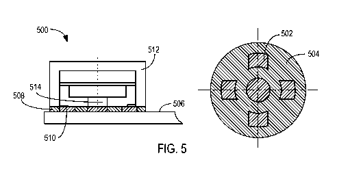
[0022] One exemplary solution to such design considerations is depicted in
FIG. 5. FIG. 5
depicts a profile and top view perspective of one embodiment 500 for providing
electrical
-11-
WO 2012/033752 CA 02810693 2013-03-06PCT/US2011/050533
connections and mechanical bonds between a battery, battery housing 412, and a
first wafer
406. The battery shown in FIG. 5 may contains the properties of the battery
shown in FIG.
4, according to one embodiment, with a cathode electrical contact 406 provided
in a central
region of the battery, and a circular anode electrical contact region
represented in FIG. 4 by
elements 404 and 408 surrounding the cathode electrical contact. For example,
in FIG. 3,
cathode electrical contacts for a given battery may be centered about position
308 or 304,
while anode electrical contacts for a given battery may form a circular region
intersecting
positions 302 or 306
[0023] Referring again to FIG. 5, battery housing 512 forms a sealed cavity
for a battery
with a first wafer 506. The cavity may be sealed and mechanically bonded
together using
several techniques alone or in combination including but not limited to fusion
bonding,
pressure bonding, anodic bonding, conductive glue bonding, laser fusion
bonding, cold
welding, ultrasonic welding, inductive welding, or laser welding. The
aforementioned
techniques may provide hermetically sealed, airtight, or otherwise enclosed
cavities to
prevent the ingress and egress of fluid or other elements with respect to
cavities holding
electronics or providing electrical connections between various electronic
components.
[0024] According to one embodiment, an intermediate layer including sections
508 and 510
may facilitate an electrical connection between a battery in housing 512 and
an electrical
component such as an ASIC (not shown) below the surface of the first wafer 406
according to
one exemplary embodiment. The intermediate layer may also at least partially
facilitate a
mechanical bonding between housing 512 and a first wafer 506 according to one
embodiment. The intermediate layer can be made out of a non-conductive
material, but not
limited to, ceramic such as A1203, peak, anodized titanium, glass coated gold,
non-
conductive glue and a conductive material, but not limited to, gold,
conductive glue or other
-12-
WO 2012/033752 CA 02810693 2013-03-06PCT/US2011/050533
metallic alloys. According to the embodiment depicted in FIG. 5, the five
cavities 502 are
aligned with electrical contacts of the battery such as electrical contact
514. As described
previously with respect to FIG. 4, the battery may include a central circular
electrical contact
406 and a second, ring shaped electrical contact defined by elements 408 and
404.
Accordingly, the cavities 502 may be aligned with these electrical contacts to
facilitate
electrical communication. Furthermore, cavities 502 facilitate electrical
communication
between the battery and an ASIC (not shown) below the first wafer 506 by
filling them with a
film of conductive glue. The cavities of conductive glue also provide
additional mechanical
bonding to facilitate a sealed environment for electronic components such as
the battery
shown in FIG. 5. In addition to conductive glue, the intermediate layer may
also comprise a
gasket 504 that are cut so as to define cavities 502. According to one
embodiment gasket 504
is made of a ceramic material and defines a sealed cavity with first wafer 506
around the
battery.
[0025] According to another exemplary embodiment depicted in FIG. 6, the
intermediate
layer as shown in FIG. 5 including a conductive glue 502 and a ceramic gasket
504 portions
further includes a hydrophobic barrier as shown by elements 606 and 612
positioned between
the central conductive glue segment of the intermediate layer electrically
connected with an
anode of the battery and the conductive glue segments electrically connected
with a cathode
of the battery. The hydrophobic barrier 606, prevents ion leakage between the
anode and
cathode portions of the battery in order to facilitate a longer battery life.
The hydrophobic
barrier 606 may be an etched ring filled with silicon oil or realized through
a specific
hydrophobic glass wafer and a battery surface treatment, according to one
embodiment.
[0026] According to another exemplary embodiment 700, depicted in FIG. 7, the
intermediate layer includes two segments of conductive glue 702 and two
segments of a glass
-13-
WO 2012/033752 CA 02810693 2013-03-06PCT/US2011/050533
formation or other isolated material 704. The glass formation or other
isolated material may
include a raised edge 708 to hold battery housing 716 onto a first wafer 706.
The glass
formation may be made according to a glass growth process that is carried out
on the surface
of first wafer 706. If raised edge 708 is an isolated material other than a
glass formation, the
isolated material may be coated with an Si02 coating, according to one
exemplary
embodiment. As in FIG. 5 and 6, the conductive glue portions associated with
the electrical
contacts of the battery such as contact 714 facilitate an electrical
connection between a
battery in housing 716 and an electrical component such as an ASIC (not shown)
below the
surface of the first wafer 706.
100271 According to another exemplary embodiment 800, depicted in FIG. 8, the
intermediate layer includes three different types of materials. A first
material includes two
segments of conductive glue 804 associated with the electrical contacts of the
battery such as
contact 820 facilitate an electrical connection between a battery in housing
818 and an
electrical component such as an ASIC (not shown) below the surface of the
first wafer 808.
The two segments of conductive glue are also depicted as elements 816 and 812
in the side
perspective view shown in FIG. 8. The intermediate layer also includes a
sealing ring 802
and 814, used to provide mechanical support for electrical connections and to
facilitate
bonding or adherence of the housing 818 to the surface of the first wafer 808.
A third
element of the intermediate layer is a bio-compatible glue 806 and 810, formed
around the
perimeter of the battery housing 818 to form a sealed cavity between the
housing 818 and the
first wafer 808. The bio-compatible glue can assist in increasing the strength
of the
mechanical connection between the housing 818 and the first wafer 808 as well
as improving
the sealing and electrical insulation of the cavity formed by housing 818 and
first wafer 808.
-14-
WO 2012/033752 CA 02810693 2013-03-06PCT/US2011/050533
[0028] According to another exemplary embodiment 900, depicted in FIG. 9, the
intermediate layer includes segments of gold coating 912 and 902. The segments
of gold
coating are associated with the electrical contacts of the battery such as
contact 916 to
facilitate an electrical connection between a battery in housing 914 and an
electrical
component such as an ASIC (not shown) below the surface of the first wafer
906. The
intermediate layer also includes as segments of glue 904 and 910, such as bio-
compatible
glue, for example. The bio-compatible glue can assist in increasing the
strength of the
mechanical connection between the housing 914 and the first wafer 906 as well
as improving
the sealing and electrical insulation of the cavity formed by housing 914 and
first wafer 906.
In the embodiment disclosed in FIG. 9, the battery contacts such as cathode
contact 916 may
be made of gold. The gold coating 902 may be bonded with the anode and cathode
gold
battery contacts according to compression bonding, anodic bonding, or a
welding process
such as cold welding, ultrasonic welding, inductive welding, or laser welding.
In addition,
the compression bonding may include different types of compression bonding
such as
thermo-compression bonding where compression takes place at temperatures above
room
temperature in order to facilitate a stronger bond.
[0029] According to one exemplary embodiment, compression bonding is used to
bond the
gold electrical contacts of battery to the gold coating 902. Under compression
bonding, the
compression causes the gold coating 902 in the intermediate layer to soften
and adhere to the
anode and cathode gold contacts of the battery as is shown by elements 406 and
404 in FIG.
4. Using the compression bonding process, temperatures can be kept under 300
C, which is a
critical temperature for certain components disposed on or between the wafers.
Accordingly,
compression bonding is an advantageous bonding technique according to some
embodiments.
-15-
WO 2012/033752 CA 02810693 2013-03-06PCT/US2011/050533
[0030] According to another exemplary embodiment 1000, depicted in FIG. 10,
the
electrical contacts of the battery 1012, 1010, and 1008 may be bonded
according to a laser
welding bonding process. Under this exemplary process, a mechanical and
electrical bond
can be formed with a first wafer 1004 using a focused laser beam to weld the
electrical
contacts, optionally with a metallic coating deposited on the first wafer
1004, together with
the battery housing. Laser fusion bonding, or laser welding, is particularly
attractive because
it involves heating only those specific areas of wafer 1004 with the battery
or battery housing.
As a result, the components attached to and/or disposed between the wafers do
not heat up
during the fusion process. In addition, to bonding metals is in discussed
previously with
respect to FIG. 10, laser fusion bonding can be used to bond one piece of
glass directly to
another piece of glass (i.e., without layers between the pieces of glass),
which eliminates
additional materials and deposition steps. Accordingly, in FIG. 10, if housing
1006 and first
wafer 904 are both made of glass, a laser welding or bonding process may be
used.
[0031] More specifically, in the laser fusion bonding process, two like
elements such as a
glass housing 1006 and a glass wafer 1004 are held in contact with each other,
and a beam
from an ultrafast, ultraviolet laser is focused at or near the interface
between the two like
elements. The laser emits picosecond or femtosecond pulses of light that heat
the wafers,
which causes the elements to melt or fuse together. Scanning the pulsed laser
beam in a
closed loop along (or just inside) the edges of housing 1006 and wafer 1004,
for example,
creates a hermetically sealed cavity for electronics such as a battery or
ASIC. The pulsed
laser beam can also be scanned in multiple closed loops to create additional
hermetically
sealed areas within the perimeter of the wafers. For example, an ASIC 118 may
be sealed in
a cavity, which itself is sealed within the perimeter of the device 100.
-16-
WO 2012/033752 CA 02810693 2013-03-06PCT/US2011/050533
[0032] According to another exemplary embodiment 1100, depicted in FIG. 11A
and 11B,
a sealed cavity for the battery is achieved by etching position grooves 1102
on a first side of a
first wafer. Subsequently, the housing of the battery can be placed in
appropriately sized
position grooves to form a sealed cavity. In addition, bio-compatible glue may
be placed
along the perimeter of the housing and the surface of the wafer to provide
more robust
mechanical bonding and sealant properties. Alternatively, as shown in FIG.
11B, the
placement of etching grooves 1106 may be placed in various positions. With
respect to the
electrical connection between the battery and an ASIC below a first wafer, the
connection
may be formed by filling feedthroughs 126 with metallic solder, according to
one
embodiment.
[0033] According to another exemplary embodiment 1200 depicted in FIG. 12A,
both the
housing 1204 and the first wafer are made of glass so that laser fusion
bonding technique can
be used to form a hermetically sealed cavity for the battery. Alternatively,
the housing 1206
may be made of a material other than glass such as metal or a ceramic that is
coated with a
glass coating of greater than 10 pm in order to use a laser fusion bonding
process. With
respect to the electrical connection between the battery and an ASIC below a
first wafer, the
connection may be formed by filling feedthroughs 126 with metallic solder,
according to one
embodiment.
[0034] According to another exemplary embodiment 1300 depicted in FIG. 13, the
electrical contact portions of the battery are directly connected to an
electrical circuit
positioned below the first wafer. In addition, a sealed cavity may be formed
between the
housing and first wafer by placing a battery lid within a gap 1304 machined or
etched into the
first wafer. The cavity may further be sealed by a lining the perimeter of the
housing and a
surface of the first wafer with a bio-compatible glue 1302. FIG 14A and 14B
depict
-17-
WO 2012/033752 CA 02810693 2013-03-06PCT/US2011/050533
additional exemplary embodiments for placing a battery protrusion or battery
lid within a
recess or cavity 1404, 1406 of a first wafer.
[0035] With respect to FIG. 15, the electrical contact portions are
electrically connected to
an integrated circuit below the first wafer through conductive rivets 1502 and
1504 such that
the rivet provides an electrical connection and is also used to bond the
battery to the surface
of the first wafer. Furthermore, the cavity containing the battery may further
be sealed by
lining the perimeter of the housing and a surface of the first wafer with a
bio-compatible glue
1506. With respect to FIG. 16, the electrical contact portions of the battery
are electrically
connected to the integrated circuit through coated wiring 1602 and the bond
between the first
wafer and the housing comprises adhering the perimeter of the housing and a
surface of the
first wafer with a bio-compatible glue.
[0036] With respect to system 1700 depicted in FIG. 17, the housing
surrounding the
battery is replaced with the first wafer 1702 that has been machined on a
second side to form
a sealed surface around the battery. In the embodiment shown in FIG. 17, the
electrical
contact portions 1708 are directly connected to the electrical circuit 1706.
Furthermore, the
electrical circuit 1706 is housed in a cavity machined into a second wafer
1704. The first and
second wafer may form a sealed cavity for the electronics contained therein
using a laser
fusion bonding process.
[0037] With respect to the embodiment 1800 depicted in FIG. 18, a cavity 1808
for an
inductive coil 122 is also provided. Embodiment 1800 includes a first wafer
1810, having a
first cavity that a battery is inserted into as well as a second wafer 1804
bonded to the first
wafer 1810 using a laser fusion bonding process such that the first wafer and
the second
wafer form a hermetically sealed cavity around the battery. Embodiment 1800
also includes
an electronic circuit 1806 that is directly connected to the electrical
contact portions of the
-18-
WO 2012/033752 CA 02810693 2013-03-06PCT/US2011/050533
battery such as cathode contact portion 1812. According to one embodiment, the
integrated
circuit is inserted into a gap in second wafer 1804 and an inductive coil 122
is inserted into a
second cavity 1808 of the first wafer wherein the inductive coil is placed on
a surface of the
third wafer 1802.
[0038] With respect to embodiment 1900 depicted in FIG. 19, a gap is machined
in the first
wafer 1904 so that an integrated circuit 1912 is fit within the gap.
Furthermore, housing 1902
is preferably metallic so that adhering the perimeter of the housing 1902 and
a surface of the
first wafer 1904 may be performed using one of a anodic bonding process and a
high
temperature bonding process prior to adhering the first wafer to the second
wafer using a
laser fusion process.
[0039] Under an anodic bonding technique, one of the glass wafers to be bonded
is coated
with a thin layer of silicon, polysilicon, tantalum, titanium, aluminum,
and/or SiNx to form a
coated glass wafer. The coated wafer is then cleaned (e.g., with isopropanol)
and dried (e.g.,
with nitrogen gas), then aligned with housing 1902 between a top tool and a
chuck which are
connected to a voltage source. Setting the voltage of the voltage source to
several hundred
volts causes current to flow from the chuck to the top tool via the coated
glass wafer 1904
and housing 1902. The current flow causes cations (e.g., alkali ions) in the
coated glass
wafer 1904 to drift towards the top tool, which acts as a cathode, and anions
in the glass
wafers to drift towards the chuck, which acts as an anode. As a result, the
region of the
housing 1902 becomes depleted of cations, and the region of the coated glass
wafer 1904 on
the other side of the coating becomes depleted of anions. This depletion
causes the surfaces
of the housing 1902 and coated glass wafer 1904 bordering the coating to
become highly
reactive, which leads to the formations of a solid chemical bond between the
wafer 1904 and
the housing 1902. -19-
WO 2012/033752 CA 02810693 2013-03-06PCT/US2011/050533
[0040] With embodiment 2000 depicted in FIG. 20, portions of the housing 2004
are coated
with a film of conductive material such as gold 2008 and the bond between the
first wafer
and the housing is formed by a cavity 2010 in a surface of the first wafer
filled with
conductive material such as gold according to one embodiment. According to one
embodiment, the gold coated portions of the housing 2008 are adhered to the
cavity 2010
using a cold weld process according to one exemplary embodiment. For various
welding and
bonding processes it is required that the film of conductive material 2008 and
the conductive
material filling gap 2010 be the same material for proper bonding. Once the
wafer and
battery housing are bonded to form a sealed cavity to form assemblies, the
assemblies may be
encapsulated in acrylic or any other suitable material 136.
[0041] The herein described subject matter sometimes illustrates different
components
contained within, or connected with, different other components. It is to be
understood that
such depicted architectures are merely exemplary, and that in fact many other
architectures
can be implemented which achieve the same functionality. In a conceptual
sense, any
arrangement of components to achieve the same functionality is effectively
"associated" such
that the desired functionality is achieved. Hence, any two components herein
combined to
achieve a particular functionality can be seen as "associated with" each other
such that the
desired functionality is achieved, irrespective of architectures or
intermediate components.
Likewise, any two components so associated can also be viewed as being
"operably
connected," or "operably coupled," to each other to achieve the desired
functionality, and any
two components capable of being so associated can also be viewed as being
"operably
couplable," to each other to achieve the desired functionality. Specific
examples of operably
couplable include but are not limited to physically mateable and/or physically
interacting
-20-
WO 2012/033752 CA 02810693 2013-03-06PCT/US2011/050533
components and/or wirelessly interactable and/or wirelessly interacting
components and/or
logically interacting and/or logically interactable components.
[0042] With respect to the use of substantially any plural and/or singular
terms herein, those
having skill in the art can translate from the plural to the singular and/or
from the singular to
the plural as is appropriate to the context and/or application. The various
singular/plural
permutations may be expressly set forth herein for sake of clarity. It will be
understood by
those within the art that, in general, terms used herein, and especially in
the appended claims
(e.g., bodies of the appended claims) are generally intended as "open" terms
(e.g., the term
"including" should be interpreted as "including but not limited to," the term
"having" should
be interpreted as "having at least," the term "includes" should be interpreted
as "includes but
is not limited to," etc.). It will be further understood by those within the
art that if a specific
number of an introduced claim recitation is intended, such an intent will be
explicitly recited
in the claim, and in the absence of such recitation no such intent is present.
For example, as
an aid to understanding, the following appended claims may contain usage of
the introductory
phrases "at least one" and "one or more" to introduce claim recitations.
[0043] However, the use of such phrases should not be construed to imply that
the
introduction of a claim recitation by the indefinite articles "a" or "an"
limits any particular
claim containing such introduced claim recitation to inventions containing
only one such
recitation, even when the same claim includes the introductory phrases "one or
more" or "at
least one" and indefinite articles such as "a" or "an" (e.g., "a" and/or "an"
should typically be
interpreted to mean "at least one" or "one or more"); the same holds true for
the use of
definite articles used to introduce claim recitations. In addition, even if a
specific number of
an introduced claim recitation is explicitly recited, those skilled in the art
will recognize that
such recitation should typically be interpreted to mean at least the recited
number (e.g., the
-21-
WO 2012/033752 CA 02810693 2013-03-06PCT/US2011/050533
bare recitation of "two recitations," without other modifiers, typically means
at least two
recitations, or two or more recitations).
[0044] The foregoing description of illustrative embodiments has been
presented for
purposes of illustration and of description. It is not intended to be
exhaustive or limiting with
respect to the precise form disclosed, and modifications and variations are
possible in light of
the above teachings or may be acquired from practice of the disclosed
embodiments. It is
intended that the scope of the invention be defined by the claims appended
hereto and their
equivalents.
-22-