Note: Descriptions are shown in the official language in which they were submitted.
CA 02812055 2013-03-11
WO 2012/037260
PCT/US2011/051605
ORGANIC SEMICONDUCTORS AS WINDOW LAYERS FOR
INORGANIC SOLAR CELLS
Cross-Reference to Related Applications
[0001] This application claims the benefit of U.S. Provisional Application
No. 61/382,885, filed September 14, 2010, the disclosure of which is
incorporated
herein by reference.
Statement Regarding Federally Sponsored Research
[0002] The subject matter of this application was prepared with U.S.
Government support under Contract No. DE-SC0001011 awarded by the
Department of Energy. The government has certain rights in the subject matter
of
this application.
Joint Research Agreement
[0003] The subject matter of this application was made by, on behalf of,
and/or in connection with one or more of the following parties to a joint
university-
corporation research agreement: University of Michigan and Global Photonic
Energy
Corporation. The agreement was in effect on and before the date the claimed
invention was made, and the claimed invention was made as a result of
activities
undertaken within the scope of the agreement.
Background
[0004] Optoelectronic devices rely on the optical and electronic
properties
of materials to either produce or detect electromagnetic radiation
electronically or to
generate electricity from ambient electromagnetic radiation.
[0005] Photosensitive optoelectronic devices convert electromagnetic
radiation into electricity. Solar cells, also called photovoltaic (PV)
devices, are a type
of photosensitive optoelectronic device that is specifically used to generate
electrical
power. PV devices, which may generate electrical energy from light sources
other
than sunlight, can be used to drive power consuming loads to provide, for
example,
lighting, heating, or to power electronic circuitry or devices such as
calculators,
radios, computers or remote monitoring or communications equipment. These
power generation applications also often involve the charging of batteries or
other
-1-
CA 02812055 2013-03-11
WO 2012/037260
PCT/US2011/051605
energy storage devices so that operation may continue when direct illumination
from
the sun or other light sources is not available, or to balance the power
output of the
PV device with a specific application's requirements. As used herein the term
"resistive load" refers to any power consuming or storing circuit, device,
equipment
or system.
[0006] Another type of photosensitive optoelectronic device is a
photoconductor cell. In this function, signal detection circuitry monitors the
resistance of the device to detect changes due to the absorption of light.
[0007] Another type of photosensitive optoelectronic device is a
photodetector. In operation a photodetector is used in conjunction with a
current
detecting circuit which measures the current generated when the photodetector
is
exposed to electromagnetic radiation and may have an applied bias voltage. A
detecting circuit as described herein is capable of providing a bias voltage
to a
photodetector and measuring the electronic response of the photodetector to
electromagnetic radiation.
[0008] These three classes of photosensitive optoelectronic devices may
be characterized according to whether a rectifying junction as defined below
is
present and also according to whether the device is operated with an external
applied voltage, also known as a bias or bias voltage. A photoconductor cell
does
not have a rectifying junction and is normally operated with a bias. A PV
device has
at least one rectifying junction and is operated with no bias. A photodetector
has at
least one rectifying junction and is usually but not always operated with a
bias. As a
general rule, a photovoltaic cell provides power to a circuit, device or
equipment, but
does not provide a signal or current to control detection circuitry, or the
output of
information from the detection circuitry. In contrast, a photodetector or
photoconductor provides a signal or current to control detection circuitry, or
the
output of information from the detection circuitry but does not provide power
to the
circuitry, device or equipment.
[0009] Traditionally, photosensitive optoelectronic devices have been
constructed of a number of inorganic semiconductors, e.g., crystalline,
polycrystalline
and amorphous silicon, gallium arsenide, cadmium telluride and others. Herein
the
term "semiconductor" denotes materials which can conduct electricity when
charge
carriers are induced by thermal or electromagnetic excitation. The term
- 2 -
CA 02812055 2013-03-11
WO 2012/037260
PCT/US2011/051605
"photoconductive" generally relates to the process in which electromagnetic
radiant
energy is absorbed and thereby converted to excitation energy of electric
charge
carriers so that the carriers can conduct, i.e., transport, electric charge in
a material.
The terms "photoconductor" and "photoconductive material" are used herein to
refer
to semiconductor materials which are chosen for their property of absorbing
electromagnetic radiation to generate electric charge carriers.
[0010] PV devices may be characterized by the efficiency with which they
can convert incident solar power to useful electric power. Device,s utilizing
crystalline
or amorphous silicon dominate commercial applications, and some have achieved
efficiencies of 23% or greater. However, efficient crystalline-based devices,
especially of large surface area, are difficult and expensive to produce due
to the
problems inherent in producing large crystals without significant efficiency-
degrading
defects. On the other hand, high efficiency amorphous silicon devices still
suffer
from problems with stability. Present commercially available amorphous silicon
cells
have stabilized efficiencies between 4 and 8%.
[0011] PV devices may be optimized for maximum electrical power
generation under standard illumination conditions (i.e., Standard Test
Conditions
which are 10001N/m2, AM1.5 spectral illumination), for the maximum product of
photocurrent times photovoltage. The power conversion efficiency of such a
cell
under standard illumination conditions depends on the following three
parameters:
(1) the current under zero bias, i.e., the short-circuit current Isc, in
Amperes (2) the
photovoltage under open circuit conditions, i.e., the open circuit voltage
Voc, in Volts
and (3) the fill factor, if.
[0012] PV devices produce a photo-generated current when they are
connected across a load and are irradiated by light. When irradiated under
infinite
load, a PV device generates its maximum possible voltage, V open-circuit, or
Voc.
When irradiated with its electrical contacts shorted, a PV device generates
its
maximum possible current, I short-circuit, or 'sc. When actually used to
generate
power, a PV device is connected to a finite resistive load and the power
output is
given by the product of the current and voltage, I x V. The maximum total
power
generated by a PV device is inherently incapable of exceeding the product, isc
x
Voc. When the load value is optimized for maximum power extraction, the
current
and voltage have the values, 'max and Vmax, respectively.
- 3 -
CA 02812055 2013-03-11
WO 2012/037260 PCT/US2011/051605
[0013] A figure of merit for PV devices is the fill factor, if, defined
as:
ff = { 'max Vmax }/{ lsc Voc (1)
[0014] where if is always less than 1, as 'Sc and Voc are never obtained
simultaneously in actual use. Nonetheless, as if approaches 1, the device has
less
series or internal resistance and thus delivers a greater percentage of the
product of
lsc and Voc to the load under optimal conditions. Where Pim is the power
incident on
a device, the power efficiency of the device, lip, may be calculated by:
rip = ff* (lsc * Voc) /Pine
[0015] To produce internally generated electric fields that occupy a
substantial volume of the semiconductor, the usual method is to juxtapose two
layers
of material with appropriately selected conductive properties, especially with
respect
to their distribution of molecular quantum energy states. The interface of
these two
materials is called a photovoltaic junction. In traditional semiconductor
theory,
materials for forming PV junctions have been denoted as generally being of
either n
or p type. Here n-type denotes that the majority carrier type is the electron.
This
could be viewed as the material having many electrons in relatively free
energy
states. The p-type denotes that the majority carrier type is the hole. Such
material
has many holes in relatively free energy states. The type of the background,
i.e., not
photo-generated, majority carrier concentration depends primarily on
unintentional
doping by defects or impurities. The type and concentration of impurities
determine
the value of the Fermi energy, or level, within the gap between the conduction
band
minimum and valance band maximum energies. The Fermi energy characterizes the
statistical occupation of molecular quantum energy states denoted by the value
of
energy for which the probability of occupation is equal to /2. A Fermi energy
near
the conduction band minimum energy indicates that electrons are the
predominant
carrier. A Fermi energy near the valence band maximum energy indicates that
holes
are the predominant carrier. Accordingly, the Fermi energy is a primary
characterizing property of traditional semiconductors and the prototypical PV
junction
has traditionally been the p-n interface.
[0016] The term "rectifying" denotes, inter alia, that an interface has
an
asymmetric conduction characteristic, i.e., the interface supports electronic
charge
transport preferably in one direction. Rectification is associated normally
with a built-
- 4 -
CA 02812055 2013-03-11
WO 2012/037260
PCT/US2011/051605
in electric field which occurs at the junction between appropriately selected
materials.
[0017] Conventional inorganic semiconductor PV cells employ a p-n
junction to establish an internal field. Early organic thin film cell, such as
reported by
Tang, Appl. Phys Lett. 48, 183 (1986), contain a heterojunction analogous to
that
employed in a conventional inorganic PV cell. However, it is now recognized
that in
addition to the establishment of a p-n type junction, the energy level offset
of the
heterojunction also plays an important role.
[0018] The energy level offset at the organic D-A heterojunction is
believed
to be important to the operation of organic PV devices due to the fundamental
nature
of the photo-generation process in organic materials. Upon optical excitation
of an
organic material, localized Frenkel or charge-transfer excitons are generated.
For
electrical detection or current generation to occur, the bound excitons must
be
dissociated into their constituent electrons and holes. Such a process can be
induced by the built-in electric field, but the efficiency at the electric
fields typically
found in organic devices (F 106V/cm) is low. The most efficient exciton
dissociation in organic materials occurs at a donor-acceptor (D-A) interface.
At such
an interface, the donor material with a low ionization potential forms a
heterojunction
with an acceptor material with a high electron affinity. Depending on the
alignment
of the energy levels of the donor and acceptor materials, the dissociation of
the
exciton can become energetically favorable at such an interface, leading to a
free
electron polaron in the acceptor material and a free hole polaron in the donor
material.
[0019] Organic PV cells have many potential advantages when compared
to traditional silicon-based devices. Organic PV cells are light weight,
economical in
materials use, and can be deposited on low cost substrates, such as flexible
plastic
foils. However, organic PV devices typically have relatively low external
quantum
efficiency (electromagnetic radiation to electricity conversion efficiency),
being on the
order of 1 % or less. This is, in part, thought to be due to the second order
nature of
the intrinsic photoconductive process. That is, carrier generation requires
exciton
generation, diffusion and ionization or collection. There is an efficiency i
associated
with each of these processes. Subscripts may be used as follows: P for power
efficiency, EXT for external quantum efficiency, A for photon absorption, ED
for
- 5 -
CA 02812055 2013-03-11
WO 2012/037260
PCT/US2011/051605
diffusion, CC for collection, and INT for internal quantum efficiency. Using
this
notation:
11P TIEXT = lA *77 * 77CC
EXT = 11A * 111NT
[0020] The diffusion length (LD) of an exciton is typically much less
(LD
50k) than the optical absorption length (-500 A), requiring a trade-off
between using
a thick, and therefore resistive, cell with multiple or highly folded
interfaces, or a thin
cell with a low optical absorption efficiency.
[0021] The performance of inorganic solar cells can be enhanced using
large bandgap window layers or heterocontact layers, which can be made of
lattice
matched III-V compounds grown on top of the GaAs and InP solar cells or oxide
and
other amorphous materials used for silicon solar cells. These layers can
improve
solar cell photo current and open circuit voltage in both Schottky barrier and
PN
junction type devices
[0022] The materials currently used for the window layers or hetero-
contact layers have been limited to inorganic semiconductors and dielectrics.
There
is disclosed herein using conducting organic materials as the window layer for
inorganic solar cells. Previously, the growth kinetics and junction
characteristics of
organic molecules on inorganic substrates have been thoroughly investigated.
It is
also shown that organic materials can passivate the inorganic material
surfaces,
reduce the dark current for photo detectors, and serve as gate dielectrics for
transistors. Researchers are also trying to use inorganic hybrid junctions for
solar
cell applications. However, the goal is adding inorganic materials into the
organic
matrix to help the exciton dissociation and charge collection. Using organic
materials
as window layers to improve inorganic solar cell performance has not been
demonstrated.
[0023] Due to the surface passivation effect and large variety of energy
levels of organic materials, they are very suitable for window layer
applications for
inorganic solar cells. As discussed herein, there is disclosed 3,4,9,10-
Perylenetetracarboxylic dianhydride (PTCDA) as the window layer for InP
Schottky
barrier solar cells. Previously, it was shown that PTCDA molecules lie flat
and can
grow into uniform thin films on inorganic semiconductor surfaces and can also
- 6 -
CA 02812055 2013-03-11
WO 2012/037260
PCT/US2011/051605
enhance the Schottky barrier heights in many cases. As discussed in more
detail
below, a thin layer of PTCDA can enhance the open circuit voltage and the
power
conversion efficiency of the InP solar cells.
Summary of the Invention
[0024] The present disclosure relates to a device comprising: an anode;
a
cathode; an inorganic substrate; and at least one organic window layer. In one
embodiment, the device comprises at least one inorganic epilayer. The organic
window layer disclosed herein is positioned between the anode and cathode,
such
as between an inorganic semiconductor layer and a contact, including between
the
anode and the at least one inorganic epilayer. In one embodiment, the
disclosed
device exhibits one or more of the following characteristics when compared to
the
device without the at least one organic window layer: increased Voc at one sun
AM1.5G illumination; increased power conversion at one sun AM1.5G
illumination;
enhanced Schottky barrier height; or reduced forward dark current.
[0025] There is also disclosed a method of enhancing the performance of
a photosensitive device having an anode, a cathode, an inorganic substrate,
and at
least one inorganic epilayer, the method comprising: positioning at least one
organic
window layer between said anode and said at least one inorganic epilayer.
[0026] In addition, there is disclosed a method of enhanced Schottky
barrier height of a photosensitive device comprising an anode, a cathode, an
inorganic substrate, and at least one inorganic epilayer, the method
comprising:
positioning at least one organic window layer between the anode and the at
least
one inorganic epilayer.
[0027] The foregoing and other features of the present disclosure will
be
more readily apparent from the following detailed description of exemplary
embodiments, taken in conjunction with the attached drawings. It will be noted
that
for convenience all illustrations of devices show the height dimension
exaggerated in
relation to the width.
Brief Description of the Drawings
[0028] Figure 1. is a schematic showing layer structures of p-InP
Schottky
barrier solar cells with 4 pm-thick lightly doped absorption region, without
3,4,9,10-
- 7 -
CA 02812055 2013-03-11
WO 2012/037260
PCT/US2011/051605
Perylenetetracarboxylic dianhydride (PTCDA) contact interfacial layer (a) and
with
PTCDA interfacial layer (b).
[0029] Figure 2. is a graph showing the measured external quantum
efficiency (EQE) of InP Schottky barrier solar cell without and with 3nm PTCDA
contact interfacial layer.
[0030] Figure 3. is a graph showing the measured current-voltage
characteristics of InP Schottky barrier solar cell with different PTCDA layer
thicknesses under dark and one sun AM1.5G condition
[0031] Figure 4. is a graph showing measured open circuit voltage at
various solar illumination power intensity of InP Schottky barrier solar cell
with
different PTCDA layer thicknesses
[0032] Figure 5. is a graph showing power conversion efficiency at
various
solar illumination power intensity of InP Schottky barrier solar cell with
different
PTCDA layer thicknesses
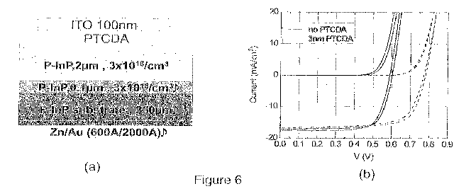
[0033] Figure 6. is a schematic showing layer structure (a) and a graph
showing current-voltage characteristics (b) of p-InP Schottky barrier solar
cells with a
2:m-thick InP lightly doped absorption region
[0034] Figure 7. is a graph showing measured energy level diagram at the
InP-PTCDA junction with ultraviolet photoemission spectroscopy. The energy
unit of
the number labeled is eV.
[0035] Figure 8. is a graph showing measured photoluminescence of p-
InP substrate without and with PTCDA capping layers of various thicknesses.
[0036] Figure 9. is a graph showing photoluminescence (excitation at
A=409nm), and excitation (emission at A=930nm) spectra of an p-InP epitaxial
wafer,
and the of the same wafer with various thicknesses (6) of 3,4,9,10-
Perylenetetracarboxylic dianhydride (PTCDA) capping layer. Inset: Energy
levels of
p-InP and PTCDA inferred from ultra-violent photoemission spectroscopy. Units
of
eV are applied to the numbers in the inset.
[0037] Figure 10. is a graph showing current density-voltage (J-V)
characteristics of p-InP/PTCDA solar cells with PTCDA window layer thicknesses
of
8=0, mm, 2nm, 4nm, and 8nm. Inset: Measured (symbols) and fit (lines) dark J-V
characteristics of p-InP/PTCDA solar cells with 6=0, 3nm, and 30nm.
- 8 -
CA 02812055 2013-03-11
WO 2012/037260
PCT/US2011/051605
[0038] Figure 11. is a graph showing external quantum efficiency (EQE)
versus wavelength for p-InP/PTCDA solar cells with PTCDA layer thicknesses of
8=0
(solid line), 3nm (dash), and 10nm (dot). The PTCDA absorption spectrum is
shown
as a reference. The EQE of devices with 24nm thick bathocuproine (BCP) (dash
dot)
and 30nm Mo03 (dash dot dot) exciton blocking layers (EBLs) between PTCDA and
ITO are also shown. Inset: Photoluminescence of PTCDA in the
Quartz/PTCDA/exciton blocking layer (EBL)/ITO structures with no EBL (solid
line),
with 12nm BCP (dash dot), and with 30nm Mo03 (dash dot dot).
Detailed Description of the Invention
[0039] As used herein, photosensitive optoelectronic devices can be
solar
cells, particularly Schottky barrier solar cell.
[0040] As used herein, the term "organic" includes polymeric materials
as
well as small molecule organic materials that may be used to fabricate organic
photosensitive optoelectronic devices. "Small molecule" refers to any organic
material that is not a polymer, and "small molecules" may actually be quite
large.
Small molecules may include repeat units in some circumstances. For example,
using a long chain alkyl group as a substituent does not remove a molecule
from the
"small molecule" class. Small molecules may also be incorporated into
polymers, for
example as a pendent group on a polymer backbone or as a part of the backbone.
Small molecules may also serve as the core moiety of a dendrimer, which
consists of
a series of chemical shells built on the core moiety. The core moiety of a
dendrimer
may be a fluorescent or phosphorescent small molecule emitter. A dendrimer may
be a "small molecule." In general, a small molecule has a defined chemical
formula
with a molecular weight that is the same from molecule to molecule, whereas a
polymer has a defined chemical formula with a molecular weight that may vary
from
molecule to molecule. As used herein, "organic" includes metal complexes of
hydrocarbyl and heteroatom-substituted hydrocarbyl ligands.
[0041] It is also appreciated that the organic materials described
herein,
whether polymeric materials or small molecule organic materials, may comprise
organic semiconductors, of either p-type or n-type.
[0042] As used herein, the term "layer" refers to a member or component
of a photosensitive device whose primary dimension is X-Y, i.e., along its
length and
- 9 -
CA 02812055 2013-03-11
WO 2012/037260
PCT/US2011/051605
width. It should be understood that the term layer is not necessarily limited
to single
layers or sheets of materials. In addition, it should be understood that the
surfaces
of certain layers, including the interface(s) of such layers with other
material(s) or
layers(s), may be imperfect, wherein said surfaces represent an
interpenetrating,
entangled or convoluted network with other material(s) or layer(s). Similarly,
it
should also be understood that a layer may be discontinuous, such that the
continuity of said layer along the X-Y dimension may be disturbed or otherwise
interrupted by other layer(s) or material(s).
[0043] The terms "electrode" and "contact" are used herein to refer to
a
layer that provides a medium for delivering photo-generated current to an
external
circuit or providing a bias current or voltage to the device. That is, an
electrode, or
contact, provides the interface between the active regions of an organic
photosensitive optoelectronic device and a wire, lead, trace or other means
for
transporting the charge carriers to or from the external circuit. Anodes and
cathodes
are examples. U.S. Patent No. 6,352,777, incorporated herein by for its
disclosure
of electrodes, provides examples of electrodes, or contacts, which may be used
in a
photosensitive optoelectronic device.
[0044] In a photosensitive optoelectronic device, it may be desirable
to
allow the maximum amount of ambient electromagnetic radiation from the device
exterior to be admitted to the photoconductively active interior region. That
is, the
electromagnetic radiation must reach a photoconductive layer(s), where it can
be
converted to electricity by photoconductive absorption. This often dictates
that at
least one of the electrical contacts should be minimally absorbing and
minimally
reflecting of the incident electromagnetic radiation. In some cases, such a
contact
should be substantially transparent. The opposing electrode may be a
reflective
material so that light which has passed through the cell without being
absorbed is
= reflected back through the cell. As used herein, a layer of material or a
sequence of
several layers of different materials is said to be "transparent" when the
layer or
layers permit at least about 50% of the ambient electromagnetic radiation in
relevant
wavelengths to be transmitted through the layer or layers. Similarly, layers
which
permit some, but less than about 50% transmission of ambient electromagnetic
radiation in relevant wavelengths are said to be "semi-transparent."
-10-
CA 02812055 2013-03-11
WO 2012/037260
PCT/US2011/051605
[0045] The term "cathode" is used in the following manner. In a non-
stacked PV device or a single unit of a stacked PV device under ambient
irradiation
and connected with a resistive load and with no externally applied voltage,
e.g., a PV
device, electrons move to the cathode from the photo-conducting material.
Similarly,
the term "anode" is used herein such that in a PV device under illumination,
holes
move to the anode from the photoconducting material, which is equivalent to
electrons moving in the opposite manner. It will be noted that as the terms
are used
herein, anodes and cathodes may be electrodes or charge transfer layers.
[0046] As used herein, "top" means furthest away from the substrate
structure (if present), while "bottom" means closest to the substrate
structure. If the
device does not include a substrate structure, then "top" means furthest away
from
the reflective electrode. For example, for a device having two electrodes, the
bottom
electrode is the electrode closest to the substrate structure, and is
generally the first
electrode fabricated. The bottom electrode has two surfaces, a bottom side
closest
to the substrate, and a top side further away from the substrate. Where a
first layer
is described as "disposed over" or "on top of" a second layer, the first layer
is
disposed further away from substrate. There may be other layers between the
first
and second layer, unless it is specified that the first layer is "in physical
contact with"
the second layer. For example, a cathode may be described as "disposed over"
or
"on top of" an anode, even though there are various organic layers in between.
[0047] It is appreciated that one does not have to have the light
incident
from the surface. Rather, it can be incident from the substrate side if there
is an
aperture (window) in the back metal contact. In other words, the top contact
can be
opaque such that the device has an inverted structure. In this embodiment, the
substrate needs to be transparent to the light that is absorbed in the
epilayer. The
top contact can also be a thin metal that is semitransparent, if light is
incident on the
top surface. It can also be any one of a number of transparent conducting
oxides
(TCO). In some embodiments, the transparent conducting oxide is chosen from
transparent oxides and metal or metal substitutes having a thickness
sufficient to
render them transparent or semi-transparent. In some embodiments, the
transparent electrode is selected from transparent conducting oxides such as
indium
tin oxide (ITO), gallium indium tin oxide (GITO), fluorine doped tin oxide
(Sn02:F or
FTO), and zinc indium tin oxide (ZITO).
-11-
CA 02812055 2013-03-11
WO 2012/037260
PCT/US2011/051605
[0048] The present disclosure relates to a device comprising: two
contacts,
typically referred to as an anode and a cathode, an inorganic substrate, such
as a
semiconductor substrate, and at least one organic window layer positioned
between
at least one contact and the inorganic substrate. It is appreciated that the
organic
window layer may be deposited directly on the substrate, or onto an inorganic
epilayer that is on top of the substrate.
[0049] Thus, while the organic window layer is broadly described as
being
positioned between the anode and cathode, it can specifically be described as
being
positioned either between the anode and the inorganic substrate, or between
the
cathode and the inorganic substrate. When an inorganic epilayer is present,
the
organic window layer is positioned between the previously mentioned contacts
(either the anode or cathode) and the inorganic epilayer.
[0050] In one embodiment the organic window layer may absorb light and
generate excitons that migrate to the inorganic where they convert to
photocurrent.
By this mechanism, the efficiency of the device is further increased.
[0051] Figure 1 shows a p-InP Schottky barrier solar cell according to
the
present invention. In this embodiment, layer structures of p-InP Schottky
barrier
solar cells are shown in cross-section, with 4 pm-thick lightly doped
absorption
region, without 3,4,9,10-Perylenetetracarboxylic dianhydride (PTCDA) contact
interfacial layer (a) and with PTCDA interfacial layer (b).
[0052] Figure 2 shows that the measured EQE versus the wavelength for
the devices with 3nm PTCDA layer and without the PTCDA layer are very similar
over the spectrum range from 400nm to 950nm. Figure 3 shows the current-
voltage
characteristics of InP solar cells with various PTCDA layer thicknesses under
dark
and one sun illumination. All devices show very similar photocurrent, which is
consistent with the similar measured EQE profiles. However, there is a
distinct
difference in the open circuit voltage (Voc) between the devices without and
with the
PTCDA window layer. Voc of the devices without PTCDA is 0.65V; while Voc of
the
devices with 4nm PTCDA layer is enhanced to 0.75V, at one sun illumination.
The
open circuit voltage versus the illumination light intensity is plotted in
Fig. 4, which
shows that the V0c of the devices with PTCDA is higher at all illumination
intensities
comparing with the device without PTCDA layer. Since there is no degradation
in fill
factors in all devices with PTCDA window layers, the power conversion
efficiency is
- 12-
CA 02812055 2013-03-11
WO 2012/037260
PCT/US2011/051605
enhanced concomitantly from 13.2 0.5% for devices without PTCDA to 15.4 0.4%
for devices with 4nm PTCDA (Fig. 5) at one sun AM1.5G illumination.
[0053] Another set of current-voltage curves for an I nP Schottky
barrier
solar cell with thinner (2pm) lightly doped absorption layer (Fig. 6 (a) is
shown in Fig.
6 (b)). The open circuit voltage of the device is enhanced from 0.62V for
devices
without PTCDA to 0.78V for devices with 3nm PTCDA window layer under one sun
illumination.
[0054] The reasons for the Vss enhancement with window layers are
manifold. To understand the function of PTCDA layer, we measured the energy
levels at the InP-PTCDA interface using Ultraviolet Photoelectron Spectroscopy
(UPS), Figure 7 shows the measured energy level diagram. The vacuum level is
shifted by 0.3eV at the InP-PTCDA interface due to a small interface dipole.
The
difference between the lowest unoccupied molecular orbital (LUMO) energy level
of
PTCDA and the InP conduction band edge (Es) is smaller than 0.1eV. The
discontinuity between the valence band edge (Ev) of InP and the highest
occupied
molecular orbital (HOMO) energy level of PTCDA is 0.8eV.
[0055] With this measured energy level alignment, the holes must
overcome a large energy barrier to go from InP to PTCDA, while the electron
conduction is not impeded at the InP-PTCDA interface. As a result, the
Schottky
diode forward biased dark current due to hole thermionic emission over the
Schottky
barrier from InP to ITO will be suppressed. Instead, the forward biased dark
current
is mainly the bulk and interface recombination current of holes in InP and
electrons
injected from ITO. The suppression of the forward dark current leads to the
enhancement of Vss.
[0056] The hole energy barrier introduced by the PTCDA layer also helps
to collect the photo-generated carriers at the right electrode, i.e.,
directing photo-
generated holes to the p+ -InP substrate instead of ITO electrode. This effect
may
not be significant at zero bias since there is a large built-in electric field
in the device
to collect the charged carriers. However, at voltages near to Võ, when the
built-in
field in the device is much lower, the photo-generated holes can diffuse to
ITO
contact and results in the loss of photo current. The PTCDA hole energy
barrier can
direct the hole diffusion to the p+ -InP substrate, which enhances the photo
current
-13-
CA 02812055 2013-03-11
WO 2012/037260
PCT/US2011/051605
near Võ as observed in the current-voltage characteristics. It also can pull
the I-V
curves down into the fourth quadrant and contributes to the enhancement of
Voc.
[0057] Another important parameter for a solar cell is the surface
recombination velocity or carrier lifetime. To qualitatively compare the
carrier
surface recombination lifetime, we measured the Photoluminescence (PL) of the
InP
films with and without PTCDA capping layers at exactly the same condition. The
results are plotted in Fig. 8. It is observed that the PL of the wafer with
PTCDA
capping layer is significantly higher than the wafer without, which indicates
a much
longer carrier lifetime. The reduction of carrier recombination and
enhancement of
carrier lifetime are essential in achieving high open circuit voltage.
[0058] The change in the Schottky barrier height may also contribute to
the
Võ enhancement. It has been shown that the effective Schottky barrier height
is
enhanced when using PTCDA interfacial layer on p-InP Schottky diodes. From our
analysis, the Voc enhancement of p-InP Schottky barrier solar cells with PTCDA
window layers is a result of multiple factors.
[0059] In the broadest sense, there is disclosed a device, such as a
Schottky barrier solar cell, comprising: an anode; a cathode; an inorganic
substrate;
and at least one organic window layer positioned between the anode and the
cathode.
[0060] In one embodiment, the device described herein exhibits one or
more of the following characteristics when compared to the device without said
at
least one organic window layer: increased Voc at one sun AM1.5G illumination;
increased power conversion at one sun AM1.5G illumination; enhanced Schottky
barrier height; and reduced forward dark current.
[0061] In one embodiment, the device described herein further comprises
at least one inorganic buffer layer positioned between the inorganic substrate
and
the at least one inorganic epilayer.
[0062] In one embodiment, the anode of the described device comprises a
transparent conducting material, such as the transparent conducting oxide
indium tin
oxide (ITO). In some embodiments, the transparent conducting oxide is chosen
from
transparent oxides and metal or metal substitutes having a thickness
sufficient to
render them transparent or semi-transparent. In some embodiments, the
-14-
CA 02812055 2013-03-11
WO 2012/037260
PCT/US2011/051605
transparent electrode is selected from transparent conducting oxides such as
indium
tin oxide (ITO), gallium indium tin oxide (GITO), fluorine doped tin oxide
(Sn02:F or
FTO), and zinc indium tin oxide (ZITO).
[0063] In one embodiment, the cathode of the described device comprises
one or more materials selected from Zn, Au, Al, Ag, alloys thereof, and stacks
thereof. For example, the cathode may comprise Zn/Au.
[0064] In another embodiment, the inorganic substrate comprises a
material selected from Ge, Si, GaAs, InP, GaN, AIN, CdTe, and combinations
thereof. Other materials that may be used include copper indium gallium
(di)selenide
(CIGS). In one embodiment, the inorganic substrate may comprise a p-type InP.
[0065] The inorganic epilayer may comprise the same materials listed
above for the inorganic substrate, including Ge, Si, GaAs, InF', GaN, AIN,
CdTe, and
combinations thereof. Other materials that may be used include copper indium
gallium (di)selenide (CIGS).
[0066] In another embodiment, the at least one inorganic buffer layer
comprises at least one III-V material, such as at least one material selected
from
GaAs and InP.
[0067] As previously stated, the at least one organic window layer may
comprise 3,4,9,10-Perylenetetracarboxylic dianhydride (PTCDA) or naphthalene
tetracarboxylic anhydride (NTCDA). In some embodiments, these crystalline
organics can be any organic semiconductor (including polymers) that are
semitransparent to the wavelengths of interest; are p-type or n-type
conducting;
and/or increase the barrier height of the p or n-type substrate. Non-limiting
examples include poly(3-hexylthiophene) (P3HT), phenyl-C61-butyric acid methyl
ester (PCBM), subphthalocyanine (SubPc), squaraine, and copper phthalocyanine
(CuPc), tin phthalocyanine (SnPc).
[0068] The least one organic layer has a thickness up to 25 rim, such as
up to 10 rim.
[0069] There is also disclosed a method of enhancing the performance of
a photosensitive device having an anode, a cathode, an inorganic substrate,
and at
least one inorganic epilayer, the method comprising: positioning at least one
organic
window layer between the anode and the at least one inorganic epilayer.
-15-
CA 02812055 2013-03-11
WO 2012/037260
PCT/US2011/051605
[0070] The method of enhancing the performance of a photosensitive
device is evidenced by the device as exhibiting one or more of the following
characteristics when compared to the device without said at least one organic
window layer: increased Voc at one sun AM1.5G illumination; increased power
conversion at one sun AM1.5G illumination; enhanced Schottky barrier height;
and
reduced forward dark current.
[0071] The method described herein comprises at least one inorganic
buffer layer positioned between the inorganic substrate and the at least one
inorganic epilayer.
[0072] In one embodiment, the anode comprises one or more materials
selected from ITO, alloys thereof, and stacks thereof.
[0073] In another embodiment, the cathode comprises any material
sufficient to make ohmic contact with the semiconductor material, such as a
metal
selected from Zn, Au, Al, alloys thereof, and stacks thereof.
[0074] In one embodiment, the inorganic substrate comprises a material
selected from Ge, Si, GaAs, InP, GaN, AIN, CdTe, and combinations thereof.
Other
materials that may be used the inorganic substrate include copper indium
gallium
(di)selenide (GIGS).
[0075] In one embodiment, the at least one inorganic epilayer comprises
at
least one III-V material, such as at least one material selected from GaAs and
InP.
[0076] In one embodiment, the at least one inorganic buffer layer
comprises at least one III-V material, the at least one inorganic buffer layer
comprises at least one material selected from GaAs and InP.
[0077] In one embodiment, the at least one organic window layer
comprises 3,4,9,10-Perylenetetracarboxylic dianhydride (PTCDA) or naphthalene
tetracarboxylic anhydride (NTCDA).
[0078] The at least one organic layer has a thickness up to lOnm.
[0079] There is also disclosed herein a method of enhancing Schottky
barrier height of a photosensitive device comprising an anode, a cathode, an
inorganic substrate, and at least one inorganic epilayer, the method
comprising:
positioning at least one organic window layer between the anode and the at
least one inorganic epilayer, wherein the device exhibits one or more of the
following
-16-
CA 02812055 2013-03-11
WO 2012/037260
PCT/US2011/051605
characteristics when compared to the device without the at least one organic
window
layer: increased Voc at one sun AM1.5G illumination; increased power
conversion at
one sun AM1.5G illumination; and reduced forward dark current.
[0080] The embodiments described herein are further illustrated by the
following non-limiting example.
Example
[0081] The epitaxial solar cell structure was grown by gas source
molecular beam epitaxy on a p-type, Zn-doped (100) InP substrate. The
epitaxial
structure consisted of a 0.1 pm thick, Be doped (3x1018 cm-3) p-type InP
buffer layer
and a 4 pm thick lightly Be doped (3x1016 cm-3) p-type InP absorption layer.
[0082] The epitaxial wafer was then fabricated into Schottky barrier
solar
cells both without PTCDA window layer and with PTCDA window layer. Right
before
the device processing, the surface of the InP epi-wafer was treated with one
minute
of NR4OH dip to remove the native oxide.
[0083] To make the conventional InP Schottky barrier solar cells, indium-
tin-oxide (ITO) electrode was directly sputtered on top of the surface-treated
InP epi-
wafer to form the structure shown in Fig. 1(a). To make the devices with PTCDA
window layer, a thin layer of PTCDA was deposited first using vacuum thermal
evaporation on the surface-treated InP epi-wafer. ITO electrode was then
sputtered
on top of the PTCDA layer under to form the device structure shown in Fig.
1(b). The
PTCDA material used in the device was purified three times using sublimation
train
purification method before the deposition.
[0084] Following growth, the epitaxial wafer was cleaned by sequential
immersion for 5 min in acetone, isopropanol maintained at 140.C, and then for
1 min
in 25% NH4OH:H20 to remove the native oxide. The back contact consisted of
20nm
Pd/5nm Zn/20nm Pd/200nm Au, and then alloyed at 400 C for lmin. Conventional
InP Schottky barrier solar cells were fabricated by ITO sputter deposition
through a
shadow mask with 1 mm-diameter circular openings. The deposition rate was
0.1A/sec for the first 100A, and then increased to 0.3A/sec to achieve a total
thickness of 1000A. The PTCDA source material was purified three times by
sublimation prior to deposition. Window layers from 8= mm to 30nm thick were
deposited by vacuum thermal evaporation at a rate of 1A/sec in a high vacuum
chamber with a base pressure <2x10⁶ Torr. The ITO sputter deposition
- 17-
CA 02812055 2013-03-11
WO 2012/037260
PCT/US2011/051605
rate and thickness for window layer devices were similar to those used for the
ITO/InP diodes.
[0085] The energy level alignment at the 01 interface was measured using
ultraviolent photoemission spectroscopy (UPS) and X-ray photoemission
spectroscopy (XPS). Photoluminescence (PL) data were obtained using a
spectrofluorometer at incident and detection angles of 45 . The diode external
quantum efficiency (EQE) was obtained using a monochromator, a lock-in
amplifier,
and a tungsten-halogen illumination source whose intensity was referenced to a
calibrated Si photodetector. The current density (J) versus voltage (V)
characteristics
were measured using a semiconductor parameter analyzer in the dark and under
simulated AM1.5G illumination. The illumination intensity was calibrated using
a
National Renewable Energy Laboratory Si reference solar cell.
[0086] Figure 9 shows the PL and excitation spectra of the InP epitaxial
layers with and without PTCDA windows. It was observed that the In P PL
intensities
of the PTCDA-coated samples are more than double that of bare InP. Now, the PL
quantum efficiency 77pL is expressed as: 17PL k rad ('cad + knr +k,),where
krad is the
radiative recombination rate, k,-is the non-radiative recombination rate in
the bulk of
semiconductor, and ks is the non-radiative surface recombination rate. Since
short
wavelength (A =409 nm) optical excitation as used in Fig. 9 primarily impacts
the
filling of surface and near-surface defects, the enhanced PL indicates a
reduced ks.
Specifically, the spectrally dependent absorption of InP suggest that the
absorption
length in InP at A = 900nm is ¨1f.im, while at A = 400nm it is only ¨20nm.
[0087] When PTCDA is deposited on InP surface, holes are injected from
the PTCDA, thereby neutralizing negatively charged traps at the InP surface.
This
increases B, as shown in Fig. 9, inset. As a result, the active surface trap
density
that accounts for the non-radiative surface recombination is reduced.
[0088] The conclusion that PTCDA reduces surface recombination is
confirmed by the excitation spectra, which show that the PL intensity
enhancement is
significantly larger at short (A<420nm) than at long wavelengths (A >580nm),
particularly when we note that 5=5nm PTCDA may attenuate the excitation signal
in
the short wavelength region. It is also observed that the PL intensity of the
PTCDA-
- 18 -
CA 02812055 2013-03-11
WO 2012/037260
PCT/US2011/051605
capped samples increases slightly with illumination over time, indicating that
surface
trap filling of the deepest levels takes several minutes to complete.
[0089] The energy level diagram of the PTCDA/InP interface, inferred
from
UPS data, is shown in the inset of Fig. 9. As-grown p-InP exhibits a surface
vacuum
level at 4.2 0.1eV relative to EF, whereas the PTCDA deposited on InP has a
vacuum level at 4.5 0.1eV. The energy band bending at the InP surface is shown
both before (dashed line, 0B=1.1 0.1eV), and after PTCDA deposition (solid
line,
0E3.=01B +6,0B). Here, AciE3 is the incremental increase in barrier height
that results from
the change in surface state charge on deposition of the PTCDA. After
depositing 5A
PTCDA, In 3d peak in InP XPS spectrum was shifted by 20meV towards higher
binding energy with respect to Fermi level, which indicates more surface band
bending and 6,0/3 is on the order of 20meV. Since the highest occupied
molecular
orbital (HOMO) energy level of PTCDA is 1.9 0.1eV below EF, the discontinuity
between the valence band maximum of InP and the PTCDA HOMO is (0.8-.6d0B) eV.
The energy difference between the lowest unoccupied molecular orbital (LUMO)
energy level of PTCDA and the InP conduction band minimum is negligible. As a
result, the photogenerated electrons in window layer cells are transported
from InP
to the ITO electrode through the PTCDA without encountering an energy barrier.
[0090] Figure 10 shows the J-V characteristics of InP solar cells with
various gin the dark, and under one sun, AM1.5G illumination. All devices with
554nm show similar photocurrent densities. However, Vos = 0.62 0.3V for
devices
without PTCDA (8=0), while Vos = 0.75 0.3V for those with 8=4nm. The power
conversion efficiency is correspondingly increased from 13.2 0.5% for 8=0 to
15.4 0.4% for those with 8= 4nm.
[0091] The forward J-V characteristics are fit using:
J Js[exp{qV __ jR=s} The fits, shown in Fig. 10 inset, yield the diode
ideality
nkT
factor, n, the specific series resistance, Rs, and the saturation dark
current, Js, as
listed in Table I together with the measured Voc.
[0092] It has been shown that the 01 interface can be modeled as a
semiconductor heterojunction to yield J= J exp(- ) ,
where Js,0 is the saturation
s
kT
-19-
CA 02812055 2013-03-11
WO 2012/037260
PCT/US2011/051605
dark current of the device without a PTCDA window layer. Assuming a short
circuit
photocurrent density of Jsc, we can write the V0 as:
vo, nkT rs, 1= nkT [ Jsc 1+ nA0B
q g
[0093] In InP-PTCDA devices, the increase in Vos is due to both a
reduced
Js and an increased n. The reduction in Js results from the increased Schottky
barrier
height with PTCDA deposition. The increased n is attributed to a reduced
forward
bias voltage across InP due to the drop across PTCDA. Note that Rs does not
increase with the increased 6, resulting in the same fill factor for devices
with and
without PTCDA.
Table I. Dark current fitting parameters
5n RsJs v
(nm) (Q.cm2) (x10-10A/cm2) (V)
0 1.31 0.80 4.8 0.62
1 1.43 1.3 AM1.5 0.71
3 1.47 0.86 AM1.5 0.75
AM1.56 0.75 4.0 0.75
AM1.56 0.83 2.6 0.76
30 AM1.59 1.0 3.6 0.76
[0094] Figure 11 shows EQE versus A for various 6 For g< 3nm, the EQE
is close to that of the ITO/InP solar cell at A> 500nm. However, at shorter
wavelengths, the EQE for PTCDA capped cells is increased due to increased
PTCDA transparency and reduced surface recombination. When 8=10nm, the EQE
is significantly decreased in the PTCDA absorption region between A = 420nm
and
580 nm. Measurements of PTCDA PL on quartz substrates indicate that excitons
generated in PTCDA are quenched by ITO deposited on its surface, as inferred
from
the PL spectra for these samples in Fig. 11, inset. To reduce quenching, a
bathocuproine (BCP) or Mo03 exciton blocking layer (EBL) is sandwiched between
- 20 -
CA 02812055 2013-03-11
WO 2012/037260
PCT/US2011/051605
the PTCDA and the ITO cathode, resulting in a significant increase in PTCDA PL
intensity. When BCP is employed in a window layer solar cell, the EQE loss at
A
=480nm disappears, whereas the use of Mo03 results in a peak at this
wavelength
that corresponds to the PTCDA absorption maximum. These results indicate that
excitons in an organic (e.g. PTCDA) can dissociate at its interface with an
inorganic
semiconductor (InP), ultimately contributing to an increased solar cell
efficiency
beyond that obtained with a conventional, "passive" window layer.
[0095] The stability of the PTCDA-InP devices has not been
systematically
tested, although we see no degradation in performance after exposure to air
for
several days. This is consistent with the observation that PTCDA is a highly
stable
organic compound.
[0096] In summary, it has been discovered that PTCDA can be used as a
window layer that both decreases the recombination rate while generating
photocurrent due to exciton dissociation at the InP surface in an
ITO/PTCDA/InP
solar cell. The solar cell power conversion efficiency is increased from 13.2
0.5% to
15.4 0.4% by using a 4 nm thick PTCDA window layer, largely due to a
concomitant
increase in Voc that arises from neutralizing InP surface states.
[0097] As generally discussed herein, and specifically exemplified in
the
above Example, organic materials can be used as window layer for inorganic
solar
cells. The Voc of p-InP Schottky barrier solar cell is enhanced by using PTCDA
as a
window layer. Without being bound by any theory, the effect is attributed to
at least
the foregoing: 1) PTCDA creates a hole energy barrier to suppress the forward
hole
thermionic emission dark current, 2) PTCDA helps to direct photo-generated
holes to
p+-InP substrate at voltages near Vim, 3) PTCDA window layer reduces the
carrier
recombination and enhances the carrier lifetime, and 4) PTCDA interfacial
layer
enhances the Schottky barrier height.
[0098] Comparing with inorganic window layers, the organic materials
have several advantages. Organic materials can be more easily deposited using
thermal evaporation or solution processing. Organic materials also have a
large
variety of energy levels, which can fit the requirements in solar cells with
different
materials and structures, where inorganic semiconductors and dielectrics
sometimes
cannot satisfy. For example, there is no good window layer for p-InP Schottky
barrier solar cell. In052A10.48As has a slightly larger bandgap, but it is not
suitable for
- 21 -
CA 02812055 2013-03-11
WO 2012/037260
PCT/US2011/051605
p-InP Schottky barrier solar cell, since it forms a electron energy barrier
and a hole
sink at the interface with InP. PTCDA has a much more suitable energy level as
a
window layer in this case.
[0099] Unless otherwise indicated, all numbers expressing quantities of
ingredients, reaction conditions, and other properties or parameters used in
the
specification are to be understood as being modified in all instances by the
term
"about." Accordingly, unless otherwise indicated, it should be understood that
the
numerical parameters set forth in the following specification and attached
claims are
approximations. At the very least, and not as an attempt to limit the
application of
the doctrine of equivalents to the scope of the claims, numerical parameters
should
be read in light of the number of reported significant digits and the
application of
ordinary rounding techniques.
[00100] Other embodiments of the invention will be apparent to those skilled
in the art from consideration of the specification and practice of the
invention
disclosed herein. It is intended that the specification and examples be
considered as
exemplary only, with a true scope and spirit of the invention being indicated
by the
following claims.
- 22 -