Note: Descriptions are shown in the official language in which they were submitted.
CA 02812371 2013-03-22
WO 2012/059251
PCT/EP2011/064085
1
FEEDBACK CONTROL OF DIMENSIONS IN NANOPORE
AND NANOFLUIDIC DEVICES
Field of the Invention
The present invention relates to the microfluidic and nanofluidic arts, and,
more particularly,
to the fabrication and use of nanoscale fluidic elements and the like.
Background of the Invention
Nanoscale fluidic devices include pores and/or channels formed in selected
substrates. A
solid-state nanopore may be fabricated through TEM (transmission electron
microscope)
drilling through a selected substrate such as silicon nitride. Solid-state
nanopores can be used
to analyze biological proteins.
Nanofluidic channels may be fabricated by serial electron beam lithography in
order to reach
the desired dimensions. Channels can also be fabricated using
photolithography, nanoimprint
lithography and nanotransfer lithography.
Summary of the Invention
Principles of the invention provide techniques for fabricating fluidic
passages such as
nanofluidic channels and nanopores. In one aspect, an exemplary method
includes the steps
of providing a substrate comprising a nanofluidic passage bounded by an
electrical
conductor, filling the nanofluidic passage with an electrolyte, and causing
the nanofluidic
passage to at least partially close by electrochemically forming an oxide
layer on the
conductor. The substrate itself can be comprised of an electrically conductive
material or an
electrically conductive material can be deposited on the substrate such that
the surface of the
nanofluidic passage comprises such material.
A further exemplary method includes the steps of providing an array of fluidic
elements,
each of the fluidic elements being connected to one or more other fluidic
elements in the
CA 02812371 2013-03-22
WO 2012/059251
PCT/EP2011/064085
2
array by one or more nanofluidic passages, each of the nanofluidic passages
including an
electrically conductive surface, and selectively closing one or more of the
nanofluidic
passages by causing an oxidized layer to electrochemically grow on the
electrically
conductive surface in selected nanofluidic passages.
A further exemplary method includes the steps of forming a nanofluidic passage
having
larger than targeted dimensions in a substrate, forming a conductive layer on
the substrate,
thereby reducing the dimensions of the nanofluidic passage, filling the
nanofluidic passage
with an electrolyte, and electrochemically oxidizing the conductive layer
until the fluidic
passage has the targeted dimensions.
Another exemplary method includes providing a nanofluidic device including a
nanofluidic
passage having an electrically conductive surface and an electrolyte within
the nanofluidic
passage and applying a voltage to the electrically conductive surface to
electrochemically
change the dimensions of the nanofluidic passage. The dimensions can be
increased or
decreased.
An exemplary computer program product is provided for controlling the
fabrication of a
nanofluidic device including a nanofluidic passage in a substrate, the
nanofluidic passage
comprising an electrically conductive surface and containing an electrolyte.
The product
includes a computer readable storage medium having computer readable program
code
embodied therewith, said computer readable program code comprising computer
readable
program code configured to facilitate applying an electric potential between
the electrolyte
and the electrically conductive surface sufficient to cause oxidation of the
electrically
conductive surface, and computer readable program code configured to monitor
ionic current
through the nanofluidic passage.
As used herein, "facilitating" an action includes performing the action,
making the action
easier, helping to carry the action out, or causing the action to be
performed. Thus, by way
of example and not limitation, instructions executing on a processor might
facilitate an
action carried out by a remote device, such as a voltage supply, meter,
microscope stage, or
the like, by sending appropriate data or commands to cause or aid the action
to be
CA 02812371 2013-03-22
WO 2012/059251
PCT/EP2011/064085
3
performed. For the avoidance of doubt, where an actor facilitates an action by
other than
performing the action, the action is nevertheless performed by some entity or
combination of
entities.
One or more embodiments of the invention or elements thereof can be
implemented in the
form of a computer program product including a tangible computer readable
recordable
storage medium with computer usable program code for performing the method
steps
indicated. Furthermore, one or more embodiments of the invention or elements
thereof can
be implemented in the form of a system (or apparatus) including a memory, and
at least one
processor that is coupled to the memory and operative to perform exemplary
method steps.
Yet further, in another aspect, one or more embodiments of the invention or
elements thereof
can be implemented in the form of means for carrying out one or more of the
method steps
described herein; the means can include (i) hardware module(s), (ii) software
module(s), or
(iii) a combination of hardware and software modules; any of (i)-(iii)
implement the specific
techniques set forth herein, and the software modules are stored in a tangible
computer-
readable recordable storage medium (or multiple such media).
Techniques of the present invention can provide substantial beneficial
technical effects. For
example, one or more embodiments may provide one or more of the following
advantages:
1) fabricating nanofluidic devices with feedback control;
2) allowing channel or pore sizes to be expanded or narrowed following
fabrication;
3) facilitating the filling of nanofluidic devices with aqueous solutions or
other liquids.
These and other features and advantages of the present invention will become
apparent from
the following detailed description of illustrative embodiments thereof, which
is to be read in
connection with the accompanying drawings.
Brief Description of the Drawings
FIGS. 1A-1D show a series of steps for fabricating a fluidic device having one
or more
channels with selected dimensions;
CA 02812371 2013-03-22
WO 2012/059251
PCT/EP2011/064085
4
FIGS. 2A-2D show a series of steps for fabricating a fluidic device having one
or more
nanopores with selected dimensions;
FIG. 3 shows the ionic current through a fluidic passage prior to and during
electrochemical
oxidation of a metal layer;
FIG. 4 shows a customizable fluidic device comprising a plurality of fluidic
elements;
FIG. 5 is a schematical illustration showing a software module for controlling
the fabrication
of nanofluidic devices;
FIG. 6 depicts a computer system that may be useful in implementing one or
more aspects
and/or elements of the invention;
FIG. 7 is a schematic illustration of a test device for changing the diameter
of a nanopore;
FIGS. 8A and 8B show a nanofilter membrane prior to and following
electrochemical
oxidation;
FIG. 9 is a schematical illustration of a fluidic device including a
nanofilter membrane, and
FIG. 10 shows a sequence of steps for fabricating a nanofilter.
Detailed Description of Preferred Embodiments
Fabrication of nanoscale fluidic elements may be difficult and can require non-
standard
and/or non-scalable techniques. The present invention allows devices to be
created using
scalable lithographic or other techniques followed by processing techniques
that provide the
desired dimensions of the fluidic passages of the elements.
Devices including nanofluidic passages such nanopores and/or nanochannels are
provided by
the invention. As discussed below, the devices may have properties that allow
customization
CA 02812371 2013-03-22
WO 2012/059251
PCT/EP2011/064085
and versatility. Principles of the invention are further employed to provide a
device
including array of fluidic elements including one or more mechanisms to
control fluid flow.
The fabrication of such devices can be facilitated by employing methods of
manufacture as
disclosed herein.
5
FIGS. 1A-1D and 2A-2D show manufacturing steps for fabricating fluidic devices
having
nanochannels and nanopores, respectively. Referring first to FIG. 1A, a
fluidic device 10 is
formed through lithographic techniques to include a channel 12 running
parallel to the
surface of the device. Lithographic techniques typically employ the use of a
photoresist that
is subjected to patterns of light while on a substrate and then removed in
part to expose
selected portions of the substrate. Subsequent etching steps and other
processing result in
features such as holes or channels being formed on the substrate. In the
exemplary device
shown in FIG. 1A, a layer 14 comprising silicon dioxide, silicon or other
suitable material(s)
is deposited on a substrate or base 16. This layer preferably has isotropic
etch characteristics.
The layer 14 may be deposited by atomic layer deposition, chemical vapor
deposition,
physical vapor deposition, thermal oxidation or other suitable procedure. The
base 16 may
be comprised, for example, of silicon, quartz, or silicon nitride, and is
different in
composition from the layer 14 deposited thereon.
A layer 20 of silicon nitride, silicon dioxide or other suitable material that
is not identical to
the material(s) comprising layer 14, is deposited on layer 14 by procedures
such as atomic
layer deposition, chemical vapor deposition, or physical vapor deposition. A
channel
opening 18 is formed in the layer 20 using lithographic techniques such as
photolithography
or electron beam lithograph. A channel 12 is formed in the layer 14 by etching
the layer 14
through the channel opening 18, The substrate or base 16 of the device
functions as an etch
stop. The channel 12 has dimensions that are larger than the dimensions that
are ultimately
desired, preferably no more than one hundred nanometers in any cross sectional
direction.
The layer 20 is laterally underetched during fabrication such that the width
of the channel
opening 18 is smaller than that of the channel 12, resulting in the device as
shown in FIG.
1A. As discussed below, the undercut beneath the top layer 20 facilitates
closing the opening
18 above the channel 12.
CA 02812371 2013-03-22
WO 2012/059251
PCT/EP2011/064085
6
The thickness of the base 16 may be between about 0.25 to 1.0mm, but is not
considered
critical. The thickness of the deposited layer 14 depends on the requirements
of the device
such as channel size. In this exemplary embodiment, the thickness of this
layer is between 10
and 1,000nm. The thickness of the top layer 20 is at least about 50nm in
thickness so that the
undercut can be formed with mechanical stability. It is preferably no thicker
than what is
required to provide such stability. The channel diameter is about one hundred
nanometers or
less prior to subsequent processing.
Referring to FIG. 1B, the fluidic device 20 is coated by a conductor 22 such
as an
electrochemically active metal. Such coating can be provided by techniques
such as atomic
layer deposition (ALD) or chemical vapor deposition (CVD). Metals such as
titanium,
tantalum, and tungsten are among the materials that can be deposited. Metal
alloys may also
be deposited. Selection of the materials may depend on the oxides that will be
formed as the
device is further processed. It will be appreciated that, in certain
circumstances, metal may
be deposited prior to channel or pore formation and that features such as
channels or pores
can formed in or through the metal through lithographical/etching techniques.
In the
exemplary embodiment, the deposited conductor 22 forms a seal to close off the
opening 18
to the channel 12. The dimensions of the channel are also reduced by an amount
commensurate with the thickness of the deposited conductor that forms the
surface of the
nanochannel.
The coated fluidic device 10 is filled with an electrolyte 24 such as water or
an electrolyte
solution as shown in FIG. IC. Filling the device is facilitated by the fact
that the channel 12
is larger than its ultimate target size (e.g. ten nm in diameter or less) even
with the conductor
coating. An electric potential may be applied to the electrolyte across the
fluidic passage to
measure the ionic current through the device. The current is proportional to
the internal
dimensions of the passage. Accordingly, the dimensions of the passage can be
determined at
this time. The electrodes for creating the ionic current are placed in or near
each end of the
fluidic passage (channel 12 in the exemplary embodiment). The electrodes may,
for
example, be Ag/AgC1, Au or Pt wire electrodes.
CA 02812371 2013-03-22
WO 2012/059251
PCT/EP2011/064085
7
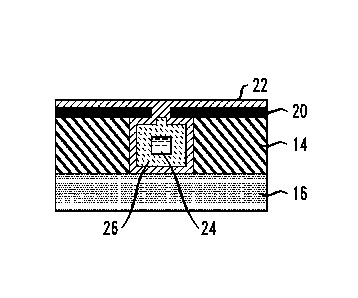
The dimensions of the channel 12 are reduced in size by forming an oxide layer
26 on the
conductor 22, as shown in FIG. 1D. This process is preferably feedback
controlled by
measuring the ionic current through the device as an electrical potential is
applied to the
conductor 22. The voltage is applied to the deposited conductor 22 using
needle probes,
alligator clips or wire bonding. Voltages may range be between 0.5 and 5.0V in
typical
applications.
FIG. 3 shows the current through the device as the oxidation layer grows from
the starting
point "A" corresponding to FIG. 1C to the end or target point "B"
corresponding to FIG. 1D.
The channel dimensions can be monitored continuously or by repeatedly
alternating
electrochemical oxidation and ionic current measurements. The process is
discontinued
when the current reaches a level representative of the target channel
dimensions, which can
be a range of acceptable dimensions. If the oxide layer 26 is insulating, the
metal-oxide stack
could then function as a gate for altering the surface charge of the device 10
for use in
further chemical functionalization, as a nanofluidic transistor, or as a
sensor device for
chemicals or biological analytes in the fluid. Such a device could also be
used as a DNA
sensor and/or sequencer. Examples of insulating metal oxides include titanium
oxides and
platinum oxides. It will be appreciated that conducting oxides could
alternatively be formed
such as aluminum zinc oxide (AZO) or ruthenium oxide.
Methods according to the invention are applicable to the formation of
nanopores running
orthogonal to the surface of the device as well as channels 12 that extend
parallel to the
surface. Referring to FIG. 2A, a device 30 includes layers 14, 16 and 20
similar to those
found in FIGS. 1A-1D. The device is fabricated in a similar manner as the
fluidic device 10
discussed above using lithographical techniques and etching. A pore 38 formed
in the top
layer 20 is in fluid communication with a reservoir 32. The pore 38 can be
substantially
larger than the target size pore, and may be as much as about 100nm in
diameter. Like the
channel 12 in the previous embodiment, the pore is accordingly in the size
range considered
nanofluidic. A pore having a diameter between two and fifty nanometers can be
formed
using a transmission electron beam. A pore ten nanometers or larger in
diameter can be
formed using electron beam or photolithographic patterning. (It will be
appreciated that the
pore may not be perfectly round, in which case the largest diameter may be
about 100nm or
CA 02812371 2013-03-22
WO 2012/059251
PCT/EP2011/064085
8
less.) A coating 40 of a conductor such as a metal or other appropriate
electrochemically
active, electrically conductive material is deposited on the device 30 as
shown in FIG. 2B.
(Such a coating may be unnecessary if the top layer 20 is comprised of an
electrochemically
active, electrically conductive material.) The pore size, though reduced by
the coating 40, is
still larger than the target size. The device is then filled with an
electrolyte 24 such as water
or an electrolyte solution. The relatively large dimensions of the fluidic
portions of the
device 30 facilitate introduction of the solution. FIG. 2C shows the fluid-
filled device. An
electrical potential is then applied to the coating 40 in order to form a
conductive or an
insulating metal-oxide film 42 as shown in FIG. 2D. The size of the pore is
monitored as
oxidation occurs. The electrochemical oxidation is discontinued when the pore
reaches the
target size. It will be appreciated that the target size may be a specific
diameter or within a
specified range. Unlike the method shown in FIGS. IA-D where the channel
opening 18 is
sealed off by the metal, the pore 38 remains open following both metal
deposition and
oxidation in order to function as a nanofluidic passage.
The formation of nanofluidic passages such as nanopores and nanofluidic
channels using the
methods described above can be accomplished on a chip by chip, completely
customized
basis. The methods can also be applied to high-throughput processing done
wafer by wafer.
The wafers can be separated into individual chips following processing. Pore
and/or channel
formation using photolithographic techniques facilitate production as opposed
to more
cumbersome procedures such as TEM drilling. Because the dimensions of the
initially
formed channels and pores are neither critical nor particularly small, initial
processing of the
chips or wafers in forming pores and/or channels is facilitated. As discussed
above, fluidic
devices having relatively large dimensions are also filled with electrolyte or
other fluid more
easily.
A test device 60 as shown in Fig. 7 can be used to demonstrate the feasibility
of the methods
disclosed herein. The device includes a five nanometer thin film 62 of TiN in
a stack
comprising layers 64, 66 of 5i02 and Si3N4, respectively. The device includes
a fluidic cell
68 containing a KC1 solution. The TiN layer includes a pore 70 less than one
hundred
nanometers in diameter and preferably smaller. About four volts are applied to
the TiN away
from the fluid volume using a contact pad and needle probe. The measured ionic
CA 02812371 2013-03-22
WO 2012/059251
PCT/EP2011/064085
9
conductance decreases significantly after a few minutes, indicating the pore
60 has decreased
in size.
Devices can be provided to end users in finished or semi-finished forms either
as chips or
wafers. The end users can perform the oxidation process to provide passages of
selected
dimensions. The oxidation process can be reversed if necessary to enlarge
passage
dimensions.
In accordance with further aspects of the invention, a generic, multipurpose
array 50 of
fluidic channels or elements 52 may be provided as shown in FIG. 4. Each
element is
connected to another element by an individually addressable, electrochemically
reducible
nanofluidic passage 54. The array is preferably fabricated with all
connections open. At the
point of use, one or more of the reducible nanofluidic passages 54 could be
closed in order to
redirect fluid flow or remove certain elements 52 from the overall array. As
shown in FIG. 4,
the original array 50 shown to the left of the figure has been modified in the
two alternative
ways to produce arrays 50A, 50B having two alternative flowpaths. Native or
partially
reduced nanofluidic passages 54 appear in solid lines while closed passages 56
are shown in
broken lines. The passages 54 may be formed in the same manner as the channels
12
discussed above. Each passage 54 includes an electrically conductive,
preferably metal
coating (not shown) having an oxide layer that defines the dimensions of the
passage.
Selected passages are closed by applying electric potential between the
electrolyte within the
passages and the metal coatings, causing further growth of the oxide layer
(not shown) until
the passage is entirely closed. The elements 52 can be designed for any
particular purpose
such as controlling or changing the properties of the fluid or of an entity
present within the
fluid. It will be appreciated that the passages 54 of the array 50 may include
only a metal
coating, allowing the end user to partially close certain passages and
completely close others
through varying degrees of oxidation of the metal coatings. As discussed
above, the
oxidation process can be reversed to open a previously closed passage 54 if
desired.
A further exemplary embodiment of the invention is shown in FIGS. 8A and 8B,
and relate
to the fabrication of a nanofilter having a large plurality of nanofluidic
passages using
principles of the invention. The nanofilter is fabricated from an electrically
conductive
CA 02812371 2013-03-22
WO 2012/059251
PCT/EP2011/064085
substrate 80. The substrate 80 includes a plurality of nanopores 82 that can
be formed using
lithographic techniques and etching. Alternatively, the nanopores can be
formed employing a
technique known as Directed Self-Assembly (DSA). This technique involves the
following
steps: (i) a substrate surface is chemically functionalized so that
nanoparticles, for example
5 block-copolymers, adhere on it upon dispersing a fluid containing such
nanoparticles onto
the substrate surface, (ii) the membrane is annealed evaporating away the
fluid leaving the
nanoparticles on the substrate surface, and (iii) the nanoparticles are then
used either as a
positive or negative hard etch mask to further transfer the nanoparticle array
pattern down
into the substrate thus forming a nanopore membrane in the substrate. Upon
flood-dispersion
10 onto the functionalized substrate surface, nanoparticles form self-
aligned pattern arrays
comprising a self-defined spacing between neighboring particles without the
need to perform
any additional alignment and/or patterning processes. Spacing thereby depends
on the type
and size of the nanoparticles, topography of the substrate surface, as well as
the type of
functionalization thereof One can achieve grating patterns as well as dot
(i.e. nanopore)
patterns.
FIG. 10 illustrates steps that can be employed for fabricating a nanofilter in
accordance with
the invention. A metal film 79 is deposited on a substrate 93 having
dielectric properties.
The filter membrane is created by removing the center portion of the substrate
93, thereby
forming an insulator 94 that supports the membrane. A pattern of nanopores 82
is formed in
the membrane portion of the metal layer 79 using techniques as described
above, thereby
providing a nanofilter substrate 80. As described further below, voltage is
applied to reduce
the pore size until a desired filter size is reached.
The pores formed in the substrate 80 of the exemplary embodiment are one
hundred
nanometers or less in diameter, and are preferably similar in size. In this
embodiment, the
substrate is comprised of an electrochemically active, electrically conductive
material. The
deposition of a metal coating on the substrate accordingly is not required. As
shown in FIG.
8A, both relatively large and small particles 84, 86 having sizes "A" and "B"
are capable of
passing through the pores. The substrate is placed in an electrolyte. A
baseline reading of
conductance or current through the substrate membrane is obtained. Voltage is
applied to the
substrate 80 to cause the formation of an oxide layer 88 on the surfaces
bounding the
CA 02812371 2013-03-22
WO 2012/059251
PCT/EP2011/064085
11
nanopores 82 as shown in FIG. 8B. When the pore sizes have been reduced to the
target
diameters, as evidenced by changes in current density or other suitable
parameter, the
process is discontinued. Referring again to FIG. 8B, the pores 82 have been
reduced in
diameter such that only the relatively small particles 86 having size "B" or
less are able to
pass therethrough. The resulting nanofilter 90 can be provided to users in the
form of a wafer
or chip or incorporated within a fluidic device. It will be appreciated that
the voltage applied
to the nanofilter 90 can be reversed, thereby increasing the diameters of the
nanopores 82. In
use, a liquid can be passed through the filter via electro-osmosis or other
suitable technique
in order to filter particles larger than the pore sizes.
FIG. 9 is a schematic illustration of a nanofluidic device including a system
that may be used
to increase or decrease pore diameters in a substrate 80 or nanofilter 90 and
provide
feedback relating to pore diameter. In this exemplary embodiment, an
electrically conductive
substrate 80 is mounted between first and second insulators 92, 94. The porous
membrane
portion of the substrate 80 is positioned within a liquid cell 98 that
contains an electrolyte.
0-rings 96 provide seals isolating part of the substrate 80 from the liquid
cell 98. An
electrical connection is made to the substrate outside the liquid cell by a
needle probe or wire
bond. A first microammeter 100 is provided for monitoring the voltage applied
to the
substrate. A second microammeter 100 is employed for measuring current through
the
substrate 80 or nanofilter 90. The second microammeter provides feedback
relating to pore
diameter as the ionic current is proportional to the sizes of the nanopores 82
in the substrate.
The oxidation or reduction process can be terminated upon obtaining a reading
from the
second microammeter that corresponds to a targeted average pore diameter. It
will be
appreciated that the measurement of the ionic current through the membrane
portion of the
substrate 80 can be expressed in units of conductance. The conductance
decreases as pore
diameter decreases.
FIG. 5 provides a schematical illustration of a system for controlling the
fabrication methods
discussed above. The system includes a nanofluidic device 110 such as those
discussed
above, a software module 112, and analog to digital/digital to analog
converter 114. The
software module includes a user interface 115 comprising a "set control
voltages" control
116, a "set endpoint conditions" control 118, a "configure and set calculation
algorithms"
CA 02812371 2013-03-22
WO 2012/059251
PCT/EP2011/064085
12
control 120, and a display 122 providing a graphical presentation of data and
process state.
The "set control voltages" control 116 allows the user to set the voltages
employed for both
oxidizing the substrate (e.g. the metal substrate 80 or coated fluidic devices
10 or 30) and
causing an ionic current through the substrate. The "set endpoint conditions"
control 118
provides the ability to automatically terminate the oxidation (or reduction)
process when the
ionic current reaches a level corresponding to a targeted nanopore or
nanochannel size. The
control 120 for configuring and setting calculation algorithms allows the user
to set the
algorithms employed in a calculation module 124. The module memory stores a
decision-
making algorithm 126 that receives input from the "set endpoint conditions"
control 118.
The decision making algorithm "control algorithms" software 126 and the "set
control
voltages" control 116 provide input to "control algorithms" software 128.
The "control algorithms" software 128 controls the voltage applied for
electrochemical
oxidation and/or reduction and process time. It further controls the voltage
for generating the
ionic current through the nanofluidic device 110 when feedback relating to
pore or channel
size is required. Inputs relating to ionic current and surface current are
provided to the
calculation module 124. The ionic conductance of the fluidic device is
determined in the
calculation module 124 which, in turn, provides conductance information to the
decision-
making algorithm software 126. As the ionic conductance information is related
to pore or
channel size, this information is provided to the decision-making algorithm
126 to determine
whether further oxidation or reduction is required. Information from the
calculation module
124 is also provided to the graphical display 122.
Given the discussion thus far, it will be appreciated that, in general terms,
an exemplary
method, according to an aspect of the invention, includes the steps of
providing a substrate
comprising a nanofluidic passage bounded by an electrical conductor, filling
the nanofluidic
passage with an electrolyte, and causing the nanofluidic passage to at least
partially close by
electrochemically forming an oxide layer on the conductor. The method is
reversible so that
the passage dimensions can be increased. The substrate itself can comprise the
electrical
conductor or an electrically conductive film can be deposited on the
substrate.
CA 02812371 2013-03-22
WO 2012/059251
PCT/EP2011/064085
13
In accordance with a further aspect of the invention an exemplary method
includes forming a
nanofluidic passage having larger than targeted dimensions in a substrate,
forming a
conductive layer on the substrate, thereby reducing the dimensions of the
nanofluidic
passage, filling the nanofluidic passage with an electrolyte, and
electrochemically oxidizing
the conductive layer until the fluidic passage has the targeted dimensions.
A further exemplary method comprises providing a nanofluidic device including
a
nanofluidic passage having an electrically conductive surface and an
electrolyte within the
nanofluidic passage and applying a voltage to the electrically conductive
surface to
electrochemically change the dimensions of the nanofluidic passage. As
discussed above, the
nanofluidic passage can comprise passages such as nanopores or nanochannels.
The method
is also applicable to changing the dimensions of a large plurality of passages
at the same
time such as passages found in the membrane of a nanofilter.
A further exemplary method relates to use of an array of fluidic elements.
Such a method
comprises providing an array of fluidic elements, each of the fluidic elements
being
connected to one or more other fluidic elements in the array by one or more
nanofluidic
passages. Each of the nanofluidic passages includes an electrically conductive
surface. The
method further comprises selectively closing one or more of the nanofluidic
passages by
causing an oxidized layer to electrochemically grow on the electrically
conductive surface in
selected nanofluidic passages. An array of fluidic elements connected by
nanofluidic
passages and a system for electrochemically changing or closing the passages
is further
provided.
A computer program product is provided for controlling the fabrication of a
nanofluidic
device that includes a nanofluidic passage in a substrate, the nanofluidic
passage comprising
an electrically conductive surface and containing an electrolyte. A computer
readable storage
medium having computer readable program code embodied therewith comprises:
computer
readable program code configured to facilitate applying an electric potential
between the
electrolyte and the electrically conductive surface sufficient to cause
oxidation of the
electrically conductive surface and computer readable program code configured
to monitor
ionic current through the nanofluidic passage.
CA 02812371 2013-03-22
WO 2012/059251
PCT/EP2011/064085
14
A nanofilter having a filter membrane including nanofluidic passages that can
be
electrochemically changed to larger or smaller sizes is further provided. As
discussed above,
the membrane can be comprised of a conductor or include a conductive coating
that can be
electrochemically oxidized. A nanofilter assembly provided as a further aspect
of the
invention preferably includes a feedback mechanism for determining the ionic
current
through the filter membrane as well as a mechanism for causing electrochemical
oxidation.
The extent to which the nanofluidic passages have been narrowed or expanded
can be
determined from the feedback mechanism. FIG. 9 provides an exemplary
embodiment of the
nanofilter assembly including a filter membrane, a mechanism for causing
oxidation, and a
mechanism for determining ionic current. FIG. 8A shows the membrane portion of
a
nanofilter that has been subjected to oxidation to reduce the size of the
nanofluidic channels.
The process can be reversed to enlarge the nanofluidic channels.
Exemplary System and Article of Manufacture Details
As will be appreciated by one skilled in the art, aspects of the present
invention may be
embodied as a system, method or computer program product. Accordingly, aspects
of the
present invention may take the form of an entirely hardware embodiment, an
entirely
software embodiment (including firmware, resident software, micro-code, etc.)
or an
embodiment combining software and hardware aspects that may all generally be
referred to
herein as a "circuit," "module" or "system." Furthermore, aspects of the
present invention
may take the form of a computer program product embodied in one or more
computer
readable medium(s) having computer readable program code embodied thereon.
One or more embodiments of the invention, or elements thereof, can be
implemented in the
form of an apparatus including a memory and at least one processor that is
coupled to the
memory and operative to perform exemplary method steps such as measuring ionic
current
and creating the electric potential used for metal layer oxidation.
One or more embodiments can make use of software running on a general purpose
computer
or workstation. With reference to FIG. 6, such an implementation might employ,
for
example, a processor 602, a memory 604, and an input/output interface formed,
for example,
CA 02812371 2013-03-22
WO 2012/059251
PCT/EP2011/064085
by a display 606 and a keyboard 608. The term "processor" as used herein is
intended to
include any processing device, such as, for example, one that includes a CPU
(central
processing unit) and/or other forms of processing circuitry. Further, the term
"processor"
may refer to more than one individual processor. The term "memory" is intended
to include
5 memory associated with a processor or CPU, such as, for example, RAM
(random access
memory), ROM (read only memory), a fixed memory device (for example, hard
drive), a
removable memory device (for example, diskette), a flash memory and the like.
In addition,
the phrase "input/output interface" as used herein, is intended to include,
for example, one or
more mechanisms for inputting data to the processing unit (for example,
mouse), and one or
10 more mechanisms for providing results associated with the processing
unit (for example,
printer). The processor 602, memory 604, and input/output interface such as
display 606 and
keyboard 608 can be interconnected, for example, via bus 610 as part of a data
processing
unit 612. Suitable interconnections, for example via bus 610, can also be
provided to a
network interface 614, such as a network card, which can be provided to
interface with a
15 computer network, and to a media interface 616, such as a diskette or CD-
ROM drive, which
can be provided to interface with media 618. Interfaces can be provided to
microammeters
and/or current supplies and the like, over a network or other suitable
interface, analog-to-
digital converter, or the like.
Accordingly, computer software including instructions or code for performing
the
methodologies of the invention, as described herein with respect to FIGS. 1A-
D, 2A-D, 8A-
B and 10 may be stored in one or more of the associated memory devices (for
example,
ROM, fixed or removable memory) and, when ready to be utilized, loaded in part
or in
whole (for example, into RAM) and implemented by a CPU. Such software could
include,
but is not limited to, firmware, resident software, microcode, and the like.
A data processing system suitable for storing and/or executing program code
will include at
least one processor 602 coupled directly or indirectly to memory elements 604
through a
system bus 610. The memory elements can include local memory employed during
actual
implementation of the program code, bulk storage, and cache memories which
provide
temporary storage of at least some program code in order to reduce the number
of times code
must be retrieved from bulk storage during implementation.
CA 02812371 2013-03-22
WO 2012/059251
PCT/EP2011/064085
16
Input/output or I/O devices (including but not limited to keyboards 608,
displays 606,
pointing devices, and the like) can be coupled to the system either directly
(such as via bus
610) or through intervening I/O controllers (omitted for clarity).
Network adapters such as network interface 614 may also be coupled to the
system to enable
the data processing system to become coupled to other data processing systems
or remote
printers or storage devices through intervening private or public networks.
Modems, cable
modem and Ethernet cards are just a few of the currently available types of
network
adapters.
As used herein, including the claims, a "server" includes a physical data
processing system
(for example, system 612 as shown in FIG. 6) running a server program. It will
be
understood that such a physical server may or may not include a display and
keyboard.
As noted, aspects of the present invention may take the form of a computer
program product
embodied in one or more computer readable medium(s) having computer readable
program
code embodied thereon. Any combination of one or more computer readable
medium(s)
may be utilized. The computer readable medium may be a computer readable
signal medium
or a computer readable storage medium. A computer readable storage medium may
be, for
example, but not limited to, an electronic, magnetic, optical,
electromagnetic, infrared, or
semiconductor system, apparatus, or device, or any suitable combination of the
foregoing.
Media block 618 is a non-limiting example. More specific examples (a non-
exhaustive list)
of the computer readable storage medium would include the following: an
electrical
connection having one or more wires, a portable computer diskette, a hard
disk, a random
access memory (RAM), a read-only memory (ROM), an erasable programmable read-
only
memory (EPROM or Flash memory), an optical fiber, a portable compact disc read-
only
memory (CD-ROM), an optical storage device, a magnetic storage device, or any
suitable
combination of the foregoing. In the context of this document, a computer
readable storage
medium may be any tangible medium that can contain, or store a program for use
by or in
connection with an instruction execution system, apparatus, or device.
CA 02812371 2013-03-22
WO 2012/059251
PCT/EP2011/064085
17
A computer readable signal medium may include a propagated data signal with
computer
readable program code embodied therein, for example, in baseband or as part of
a carrier
wave. Such a propagated signal may take any of a variety of forms, including,
but not
limited to, electro-magnetic, optical, or any suitable combination thereof A
computer
readable signal medium may be any computer readable medium that is not a
computer
readable storage medium and that can communicate, propagate, or transport a
program for
use by or in connection with an instruction execution system, apparatus, or
device.
Program code embodied on a computer readable medium may be transmitted using
any
appropriate medium, including but not limited to wireless, wireline, optical
fiber cable, RF,
etc., or any suitable combination of the foregoing.
Computer program code for carrying out operations for aspects of the present
invention may
be written in any combination of one or more programming languages, including
an object
oriented programming language such as Java, Smalltalk, C++ or the like and
conventional
procedural programming languages, such as the "C" programming language, BASIC
programming language, or similar programming languages. The program code may
execute
entirely on the user's computer, partly on the user's computer, as a stand-
alone software
package, partly on the user's computer and partly on a remote computer or
entirely on the
remote computer or server. In the latter scenario, the remote computer may be
connected to
the user's computer through any type of network, including a local area
network (LAN) or a
wide area network (WAN), or the connection may be made to an external computer
(for
example, through the Internet using an Internet Service Provider).
Aspects of the present invention are described herein with reference to
flowchart illustrations
and/or block diagrams of methods, apparatus (systems) and computer program
products
according to embodiments of the invention. It will be understood that each
block of the
flowchart illustration and/or block diagram, such as provided in FIG. 5, and
combinations of
blocks in the flowchart illustration and/or block diagram, can be implemented
by computer
program instructions. These computer program instructions may be provided to a
processor
of a general purpose computer, special purpose computer, or other programmable
data
processing apparatus to produce a machine, such that the instructions, which
execute via the
CA 02812371 2013-03-22
WO 2012/059251
PCT/EP2011/064085
18
processor of the computer or other programmable data processing apparatus,
create means
for implementing the functions/acts specified in the flowchart and/or block
diagram block or
blocks.
These computer program instructions may also be stored in a computer readable
medium
that can direct a computer, other programmable data processing apparatus, or
other devices
to function in a particular manner, such that the instructions stored in the
computer readable
medium produce an article of manufacture including instructions which
implement the
function/act specified in the flowchart and/or block diagram block or blocks.
The computer program instructions may also be loaded onto a computer, other
programmable data processing apparatus, or other devices to cause a series of
operational
steps to be performed on the computer, other programmable apparatus or other
devices to
produce a computer implemented process such that the instructions which
execute on the
computer or other programmable apparatus provide processes for implementing
the
functions/acts specified in the flowchart and/or block diagram block or
blocks.
The flowchart and block diagram in the Figures illustrate the architecture,
functionality, and
operation of possible implementations of systems, methods and computer program
products
according to various embodiments of the present invention. In this regard,
each block in the
flowchart or block diagrams may represent a module, segment, or portion of
code, which
comprises one or more executable instructions for implementing the specified
logical
function(s). It should also be noted that, in some alternative
implementations, the functions
noted in the block may occur out of the order noted in the figures. For
example, two blocks
shown in succession may, in fact, be executed substantially concurrently, or
the blocks may
sometimes be executed in the reverse order, depending upon the functionality
involved. It
will also be noted that each block of the block diagrams and/or flowchart
illustration, and
combinations of blocks in the block diagrams and/or flowchart illustration,
can be
implemented by special purpose hardware-based systems that perform the
specified
functions or acts, or combinations of special purpose hardware and computer
instructions.
CA 02812371 2013-03-22
WO 2012/059251
PCT/EP2011/064085
19
It should be noted that any of the methods described herein can include an
additional step of
providing a system comprising distinct software modules embodied on a computer
readable
storage medium; the modules can include, for example, any or all of the
elements depicted in
the block diagram and/or described herein; by way of example and not
limitation, an
initialization module, a module to cycle through the test points and
parameters, an output
module to generate the output file, a post-processing module to reduce the
data and search
for anomalies, and the like. The method steps can then be carried out using
the distinct
software modules and/or sub-modules of the system, as described above,
executing on one or
more hardware processors 602. Further, a computer program product can include
a
computer-readable storage medium with code adapted to be implemented to carry
out one or
more method steps described herein, including the provision of the system with
the distinct
software modules
In any case, it should be understood that the components illustrated herein
may be
implemented in various forms of hardware, software, or combinations thereof;
for example,
application specific integrated circuit(s) (ASICS), functional circuitry, one
or more
appropriately programmed general purpose digital computers with associated
memory, and
the like. Given the teachings of the invention provided herein, one of
ordinary skill in the
related art will be able to contemplate other implementations of the
components of the
invention.
The terminology used herein is for the purpose of describing particular
embodiments only
and is not intended to be limiting of the invention. As used herein, the
singular forms "a",
"an" and "the" are intended to include the plural forms as well, unless the
context clearly
indicates otherwise. It will be further understood that the terms "comprises"
and/or
"comprising," when used in this specification, specify the presence of stated
features,
integers, steps, operations, elements, and/or components, but do not preclude
the presence or
addition of one or more other features, integers, steps, operations, elements,
components,
and/or groups thereof.
The corresponding structures, materials, acts, and equivalents of all means or
step plus
function elements in the claims below are intended to include any structure,
material, or act
CA 02812371 2013-03-22
WO 2012/059251
PCT/EP2011/064085
for performing the function in combination with other claimed elements as
specifically
claimed. The description of the present invention has been presented for
purposes of
illustration and description, but is not intended to be exhaustive or limited
to the invention in
the form disclosed. Many modifications and variations will be apparent to
those of ordinary
5 skill in the art without departing from the scope and spirit of the
invention. The embodiment
was chosen and described in order to best explain the principles of the
invention and the
practical application, and to enable others of ordinary skill in the art to
understand the
invention for various embodiments with various modifications as are suited to
the particular
use contemplated.