Note: Descriptions are shown in the official language in which they were submitted.
CA 02813942 2013-04-05
WO 2011/044333 PCT/US2010/051779
Antenna System Providing High Isolation between Antennas on
Electronics Device
CROSS REFERENCE TO RELATED APPLICATIONS
[0001] This application claims priority from (1) U.S. Provisional Patent
Application
Serial No. 61/250,344 filed on October 9,2009 and entitled "Balanced Antenna
and
Arrangement for Obtaining High Isolation between Antennas on the Same
Electronics
Device" and (2) U.S. Provisional Patent Application Serial No. 61/363,085
filed on July 9,
2010 and entitled "Antenna With Reduced Near-Field Radiation And Specific
Absorption
Rate (SAR) Values," both of which are hereby incorporated by reference.
BACKGROUND
[0002] The present application relates generally to antenna systems in
portable
electronics devices having two or more antennas operating simultaneously.
[0003] Portable electronics devices (e.g., USB Dongles and other wireless
routers,
cellular handsets, personal digital assistants, smart phones, and portable
personal
computers) typically include electronics components on a printed circuit board
(PCB)
assembly. Antennas for radio communications to and from such a device may be
attached
to the PCB assembly. For example, single-ended antennas may be fed directly
from the
PCB assembly, which then serves as a counterpoise for the antennas, allowing
the antennas
to be much smaller than otherwise possible. When the counterpoise is small
(e.g., with
dimensions on the order of the operating wavelength of the antennas or less),
feeding two or
more antennas from the same counterpoise can have the disadvantage of
introducing too
much coupling from one antenna to another. This is an example of a coexistence
problem
where more than one radio must operate at the same time from the same device.
[0004] One example of a device having two or more antennas fed from the same
counterpoise is a portable wireless router device using a first radio for
communication with
a wide area network (WAN) using WiMAX in the 2500 to 2700 MHz band, and a
second
radio for local area network (LAN) communication using 802.11 (WiFi) protocols
in the
2400 to 2500 MHz band. It is desirable to obtain as much isolation as possible
between the
- 1 -
CA 02813942 2013-04-05
WO 2011/044333 PCT/US2010/051779
antenna(s) connected to the WiMAX radio and the antenna(s) connected to the
WiFi radio
because the adjacent operating bands make the radios particularly vulnerable
to interfering
with each other.
[0005] Additionally, industrial design trends for portable electronics devices
are
driving slimmer form factors. At the same time, advanced communications
systems using
multiple-input, multiple-output (MIMO) signal processing techniques are
driving multiple
radio transmitters onto these platforms. The combination of two or more radios
and a slim
form factor creates significant difficulties in meeting Specific Absorption
Rate (SAR)
regulatory requirements.
BRIEF SUMMARY OF EMBODIMENTS OF THE INVENTION
[0006] In accordance with one or more embodiments, an antenna system is
provided
in a portable electronics device. The antenna system includes a first antenna
and a second
balanced antenna provided on the printed circuit board assembly of the
portable electronics
device. The first antenna is fed from a portion of the printed circuit board
assembly such
that a ground plane of the printed circuit board assembly serves as a
counterpoise for the
first antenna. The second balanced antenna has dipole ends configured and
oriented to
generally minimize coupling to the ground plane of the printed circuit board
assembly to
increase isolation between the first antenna and the second balanced antenna.
[0007] Various embodiments of the invention are provided in the following
detailed
description. As will be realized, the invention is capable of other and
different
embodiments, and its several details may be capable of modifications in
various respects,
all without departing from the invention. Accordingly, the drawings and
description are to
be regarded as illustrative in nature and not in a restrictive or limiting
sense.
BRIEF DESCRIPTION OF THE DRAWINGS
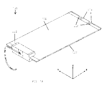
[0008] FIG. lA is a perspective view of an exemplary antenna system in
accordance
with one or more embodiments.
[0009] FIG. 1B is a cross section view of the antenna system of FIG. 1A.
- 2 -
CA 02813942 2013-04-05
WO 2011/044333 PCT/US2010/051779
[0010] FIG. 1C is an enlarged perspective view of the balanced antenna shown
in
FIG. 1A.
[0011] FIG. 1D is an enlarged perspective view of the balanced antenna of FIG.
1C
with the carrier removed for purposes of illustration.
[0012] FIGS. 2A-2C are graphs illustrating return loss and coupling measured
between the test ports of the antenna system of FIG. 1A.
[0013] FIGS. 3A-3C illustrate measured radiation patterns for the balanced
antenna
of the antenna system of FIG. 1A.
[0014] FIG. 4 is a perspective view of an alternative antenna system in
accordance
with one or more embodiments.
[0015] FIGS. 5A-5D are graphs illustrating return loss and coupling measured
between the test ports of the antenna system of FIG. 4.
[0016] FIG. 6A is a perspective view of an alternate antenna system in
accordance
with one or more embodiments.
[0017] FIG. 6B is a perspective view of the antenna system of FIG. 6A showing
the
balanced antenna separated from the printed circuit board assembly for
purposes of
illustration.
[0018] FIG. 6C is a cross-section view of the antenna system of FIG. 6A
showing
the balanced antenna separated from the printed circuit board assembly for
purposes of
illustration.
[0019] FIGS. 7A-7D are graphs illustrating various antenna performance
parameters for the antenna system of FIG. 6A.
[0020] FIG. 8 is a perspective view of an antenna system in accordance with
one or
more alternate embodiments.
[0021] FIG. 9 is a perspective view of an antenna system in accordance with
one or
more alternate embodiments.
- 3 -
CA 02813942 2013-04-05
WO 2011/044333 PCT/US2010/051779
[0022] Like reference numerals generally represent like parts in the drawings.
DETAILED DESCRIPTION
[0023] Various embodiments disclosed herein are directed to antenna systems
for
electronic communications devices having two or more antennas operating
simultaneously.
As discussed in greater detail below, the antenna system includes a printed
circuit board
assembly having a ground plane and a first antenna and a second balanced
antenna provided
on the printed circuit board assembly. The first antenna is fed from a portion
of the printed
circuit board assembly such that the ground plane of the printed circuit board
assembly
serves as a counterpoise for the first antenna. The second balanced antenna
has dipole ends
configured and oriented to generally minimize coupling to the ground plane of
the printed
circuit board to increase isolation between the first antenna and the second
balanced
antenna. In one or more embodiments, the peak near fields created by each
antenna do not
substantially overlap, thereby reducing the increase in SAR that may otherwise
occur when
both antennas are used to transmit simultaneously.
[0024] FIGS. 1A-1D illustrate an antenna system assembly 100 in accordance
with
one or more embodiments. In this example, the assembly comprises a 60 x 100 mm
PCB
102 and three antennas. The PCB 102 is representative of a PCB that may be
used to hold
the electronics of a portable WiMAX/WiFi device. Two WiMAX antennas 104 are
attached to one end of the PCB 102. The WiMAX antennas 104 are fed from the
edge of
the PCB 102 (at feed points 110) such that the ground plane 108 of the PCB 102
serves as
the counterpoise for both antennas 104.
[0025] A third balanced antenna 112, generally optimized for operation in the
WiFi
frequency band, is located at the opposite end of the PCB 102. The antenna
112, shown in
the side cross-section view of FIG. 1B and isometric view of FIG. 1C, is
formed using a
copper foil pattern 114 applied to a plastic supporting piece or carrier 116.
Connection to
the feed point can be made with a 1.1 mm diameter coaxial cable 118. A feed
terminal 120
is connected to the shield of the coaxial cable 118, and a feed terminal 122
is connected to
the center conductor of the coaxial cable 118. The balanced antenna 112 is
oriented to
produce far E-field polarization normal to the ground plane 108. Referring to
FIG. 1A, the
PCB 102 and associated ground plane 108 lie in the X-Y plane, and the balanced
antenna
112 is oriented to produce far E-field polarization aligned with the Z-axis.
- 4 -
CA 02813942 2013-04-05
WO 2011/044333 PCT/US2010/051779
[0026] FIG. 1D shows the WiFi antenna 112 with the carrier 116 removed for
purposes of illustration. The antenna 112 comprises a center-fed dipole with
capacitive end
plates 124 and an inductive connection 126 between ends. The end plates 124
serve to
lower the resonant frequency of the antenna 112 so that the antenna 112 can be
much
shorter than the nominal half-wavelength dipole. A short dipole has lower
input impedance
than a half-wave dipole and the inductive connection serves to increase the
real input
impedance of the antenna 112 to match to 50-ohms. In this example, the antenna
height, or
z-axis dimension, is 10 mm or 1/12 wavelength at 2500 MHz, making it amenable
to
embedding within a low-profile product.
[0027] Because the antenna 112 is balanced, it does not require connection to
a
counterpoise. Nonetheless even if the antenna 112 is not intentionally
connected to the
PCB ground 108, it will readily couple to the PCB ground 108 through near
field
interaction without specific arrangement avoid this effect. To reduce
coupling, the antenna
112 is placed generally symmetrically about the PCB ground 108 in the z-axis,
as can be
seen from the side view of the assembly of FIG. 1B. In this way, the dipole
ends, which are
at electric potentials of equal magnitude but opposite sign, are equidistant
from the ground
plane 108 and result in neutral potential at the ground plane 108, and
consequentially the
net coupling to the ground plane is zero. If the dipole is offset in the z-
axis, then a net
potential can be imparted to the end of the ground plane 108. This could
undesirably
couple to horizontal resonance modes of the ground plane 108 and hence to the
antennas
104 for which the ground plane 108 is serving as counterpoise, and thereby
couple the
antennas 104, 112.
[0028] The design and arrangement of the balanced antenna 112 to avoid
coupling
to the PCB ground 108 has several advantages, including, as stated above, that
the coupling
to other antennas 104 that already interact with the PCB ground 108 is
reduced. In
addition, the pickup of noise or other unwanted conducted signals from the PCB
ground
108 is also reduced. Furthermore, scattering by the PCB ground 108 is reduced,
such that
the embedded dipole maintains the omni-directional azimuth pattern of a free-
space dipole.
Refer to the theta=90 degrees plot of the measured radiation patterns for the
balanced
antenna 112 provided in FIG. 3C.
- 5 -
CA 02813942 2013-04-05
WO 2011/044333 PCT/US2010/051779
[0029] Plots of measured S parameters for a prototype of the assembly of FIG.
lA
are shown in FIGS. 2A-2C. For these plots, the Port 1 is connected to the
balanced antenna
112 and Ports 2 and 3 are connected to the WiMAX antennas 104. Coupling
between the
balanced antenna 112 and WiMAX antennas 104 (S12 and S13) is between
-28 and -40 dB. By contrast, coupling between the two WiMAX antennas 104 on
the PCB
is about -15 dB.
[0030] FIG. 4 illustrates an antenna system 400 in accordance with one or more
alternate embodiments, which uses the same two WiMAX antennas 104 but with a
two-port
balanced WiFi antenna 402. The two-port balanced antenna 402 is a two-port
antenna
designed to provide generally optimal isolation between the two WiFi ports and
is similar to
antennas described in U.S. Patent Nos. 7,688,273 and 7,688,275, the contents
of which are
hereby incorporated by reference herein. In general, the second balanced
antenna 402
includes two antenna elements 404, 406, each operatively coupled to a
respective antenna
port 408, 410. A connecting element 412 electrically connects the antenna
elements 404,
406 such that electrical currents on one antenna element flow to the other
antenna element
and generally bypass the antenna port coupled to the other antenna element.
The electrical
currents flowing through each antenna element are generally equal in
magnitude, such that
an antenna mode excited by one antenna port is generally electrically isolated
from a mode
excited by the other antenna port at a given desired signal frequency range.
[0031] In the FIG. 4 example, the balanced antenna 402 is designed to produce
z-
axis polarization, with low profile (10 mm height) and symmetry about the
plane of the
PCB ground.
[0032] Plots of simulated S parameters for a model of the assembly of FIG. 4
are
included as FIGS. 5A-5D. For these plots, the Ports 1 and 2 are connected to
the WiMAX
antennas, and Ports 3 and 4 are connected to the balanced two-port antenna.
Coupling
between the WiMAX antennas (S12) is about -15 dB as before (FIG. 5A). For the
two-
port antenna, both ports are well matched and have enhanced isolation over the
WiFi band
(2400 to 2500 MHz). The coupling between WiMAX and either WiFi antenna port is
less
than 35 dB (FIGS. 5C and 5D). This antenna configuration therefore provides
adequate
isolation for co-existence between WiFi and WiMAX radios, while allowing full
MIMO or
diversity operation within the 802.11n or 802.11b protocols.
- 6 -
CA 02813942 2013-04-05
WO 2011/044333 PCT/US2010/051779
[0033] FIGS. 6A-6C illustrate an antenna system 600 in accordance with one or
more further embodiments. The antenna system can be used, e.g., in a USB
dongle
assembly for communication over WiMAX. The antenna system 600 includes a
printed
antenna 602 (that uses the ground plane 604 of a printed circuit board
assembly as a
counterpoise) and a balanced antenna 606. Both antennas are located at the
same end of
the PCB assembly as shown in FIG. 6B. The balanced antenna 606 in this example
is
formed by wrapping a flexible printed circuit (FPC) onto a plastic carrier
608. The plastic
carrier 608 can be slid onto the end of the PCB. Spring contacts 610 on the
top and bottom
side of the PCB provide connection to the feed and ground terminals of the
balanced
antenna, respectively, as depicted in FIG. 6C.
[0034] Plots of antenna performance parameters VSWR, S12, efficiency, and
antenna cross-correlation are provided as FIGS. 7A-7D. These plots demonstrate
good
performance across the entire band from 2500 to 2700 MHz.
[0035] FIG. 8 is a perspective view of an alternate antenna system 800 in
accordance with one or more embodiments. The antenna system 800 includes a
balanced
antenna 802 that is formed from a single piece of stamped metal. The balanced
antenna can
be attached to the PCB, e.g., by sliding it onto the PCB. For simplicity,
antennas coupled to
the ground plane of the printed circuit board are not shown in FIG. 8.
[0036] FIG. 9 is a perspective view of another alternative antenna system 900
in
accordance with one or more embodiments. The antenna system includes a
balanced
antenna that is formed from two pieces of stamped metal 902, each forming a
half of the
balanced antenna. A balanced antenna is completed by attaching the two pieces
902 (e.g.,
by soldering) to the top and bottom sides of a PCB 904. Each antenna piece has
two legs.
The legs on one side of the stamped pieces are soldered to pads on the PCB 904
that are
connected together. The connected pads thereby complete the inductive
connection
between the top and bottom halves 902 of the balanced antenna. The ends of the
legs on
the other side of the pieces serve as the antenna feed terminals. One terminal
is attached to
the top side of the PCB 904 and the opposite terminal is attached to the
bottom side of the
PCB 904. For simplicity, antennas coupled to the ground plane of the printed
circuit board
are not shown in FIG. 9.
- 7 -
CA 02813942 2013-04-05
WO 2011/044333 PCT/US2010/051779
[0037] Another advantage of antenna systems in accordance with various
embodiments is that they produce reduced SAR values for devices that
simultaneously
transmit from two antennas, thereby facilitating compliance with SAR
regulations.
[0038] It is common for two or more antennas in portable electronics devices
to use
the PCB ground plane as a counterpoise. Since the PCB ground plane is
typically the
largest conductor in the device, it tends to dominate the radiation
environment. The near
field distribution is also dominated by this feature. If two antennas are
coupled to the same
ground plane and are in close proximity to each other (i.e., less than a
quarter of a
wavelength apart), their near-field distributions will be largely overlapping.
Connecting
two transmitters, one to each antenna, will effectively double the resultant
near-field (as
compared to a single transmitter). In turn, the SAR values will also double.
[0039] This problem is mitigated by antenna systems in accordance with various
embodiments because they provide increased isolation between antennas (one
coupled to
the main PCB ground as a counterpoise and a separate antenna that is balanced
on and is
not coupled into the PCB ground). The antenna system is configured such that
the resultant
near field distribution created by each antenna does not substantially
overlap. As
mentioned above, SAR values can double for overlapping near fields. However,
SAR
values are reduced in exemplary embodiments, e.g., to 1.5 times that of a
single transmitter,
which is preferable and is achieved from an antenna configuration that reduces
the
overlapping region of the near-field from each antenna.
[0040] By way of example, in the antenna system of FIG. 6A, the peak SAR
locations of the printed antenna and those for the balanced antenna are
generally not
coincident. In particular, for the printed antenna, the peak SAR is found
around a
circumference about the PCB assembly near the location between the antenna and
the
grounded PCB assembly. On the other hand, the peak SAR location for the
balanced
antenna is off the end of PCB assembly.
[0041] It is to be understood that although the invention has been described
above
in terms of particular embodiments, the foregoing embodiments are provided as
illustrative
only, and do not limit or define the scope of the invention. Various other
embodiments,
including but not limited to the following, are also within the scope of the
claims. For
example, elements and components described herein may be further divided into
additional
- 8 -
CA 02813942 2013-04-05
WO 2011/044333 PCT/US2010/051779
components or joined together to form fewer components for performing the same
functions.
[0042] Having described preferred embodiments of the present invention, it
should
be apparent that modifications can be made without departing from the spirit
and scope of
the invention.
- 9 -