Note: Descriptions are shown in the official language in which they were submitted.
CA 02815068 2013-04-17
WO 2012/058123
PCT/US2011/057383
ELECTRO-OPTIC DEVICE WITH GAP-COUPLED ELECTRODE
STATEMENT AS TO RIGHTS TO INVENTIONS MADE UNDER
FEDERALLY SPONSORED RESEARCH OR DEVELOPMENT
[0001] The United States Government has rights in this invention pursuant to
Contract No.
DE-AC52-07NA27344 between the U.S. Department of Energy and Lawrence Livermore
National Security, LLC, for the operation of Lawrence Livermore National
Laboratory.
BACKGROUND OF THE INVENTION
[0002] Current optical switch technologies for high energy/high power laser
beams use an
electro-optical Pockels Cell based on deuterated potassium dihydrogen
phosphate (DKDP)
switch crystals, with electric fields applied either in a longitudinal or
transverse orientation as
shown in FIG. 1. The applied electric field changes the polarization of light
beam, and the
polarization changes can be converted to intensity modulation and redirection
using external
polarizers. Devices based on transverse electrode geometries have two
drawbacks: they
require a large switching voltage (>55 kV at a 25 cm aperture) that increases
with aperture
size; and the appropriate crystal orientation to achieve electro-optic
switching results in an
anisotropic optical refractive index in the aperture plane (birefringence),
which induces
undesired polarization rotation. This birefringence is typically compensated
for by using a
pair of two matched devices, which typically requires stringent matching of
the thicknesses of
both crystals to better than 1 [an.
[0003] FIG. 1 illustrates definitions for crystal, aperture, and electric
field orientations.
The longitudinal electric field (E-field) is parallel to the optical
propagation direction z, while
transverse E-field (along x) is perpendicular to the optical propagation. The
optical input has
a finite transverse extent in the x-y plane, described by the optical
aperture. The crystal
thickness is measured along the propagation direction z.
[0004] Despite the advances made in high power optical switches, there is a
need in the art
for improved methods and system related to optical switches.
1
CA 02815068 2013-04-17
WO 2012/058123
PCT/US2011/057383
SUMMARY OF THE INVENTION
[0005] According to the present invention, techniques related to optical
systems are
provided. More particularly, embodiments of the present invention relate to
systems for
high-power Pockels cells and methods of operating the same. Merely by way of
example, the
invention has been applied to a Pockels cell with transparent electrodes
disposed on
substrates spatially separated from the electro-optic crystal. The methods and
systems
described herein are also applicable to other optical systems suitable for use
with amplifier
and laser systems.
[0006] According to an embodiment of the present invention, an electro-optic
device is
provided. The electro-optic device includes an electro-optic crystal having a
predetermined
thickness and a face and an electrode substrate disposed opposing the face.
The electrode
substrate includes a substrate material having a thickness and an electrode
coating coupled to
the substrate material. The electro-optic device also includes a voltage
source electrically
coupled to the electrode coating.
[0007] According to another embodiment of the present invention, an electro-
optic device
is provided. The electro-optic device includes an electro-optic crystal having
a
predetermined thickness, a first face, and a second face. The electro-optic
device also
includes a first electrode substrate disposed opposing the first face. The
first electrode
substrate includes a first substrate material having a first thickness and a
first electrode
coating coupled to the first substrate material. In an embodiment, the first
electrode coating
is deposited on the first substrate material. The electro-optic device further
includes a second
electrode substrate disposed opposing the second face. The second electrode
substrate
includes a second substrate material having a second thickness and a second
electrode coating
coupled to the second substrate material. In an embodiment, the second
electrode coating is
deposited on the second substrate material. Additionally, the electro-optic
device includes a
voltage source electrically coupled to the first electrode coating and the
second electrode
coating. The voltage source is operable to apply an electric field across the
electro-optic
crystal.
[0008] According to yet another embodiment of the present invention, a method
of
operating a Pockels cell is provided. The method includes providing a Pockels
cell having a
first electrode substrate having an input surface, an output surface, and a
first electrode
coating coupled to the output surface. The Pockels cell also has an electro-
optic crystal
disposed adjacent to the first electrode substrate and a second electrode
substrate having an
input surface, an output surface, and a second electrode coating coupled to
the input surface.
2
CA 02815068 2013-04-17
WO 2012/058123
PCT/US2011/057383
The method also includes directing an input beam having a first polarization
state to impinge
on the input surface of the first electrode substrate, passing at least a
portion of the input
beam through the first electrode substrate, and passing at least a portion of
the input beam
through the first electrode coating. The method further includes applying a
voltage between
the first electrode coating and the second electrode coating and changing the
first polarization
state into a second polarization state using the electro-optic crystal.
Additionally, the method
includes passing at least a portion of the input beam through the second
electrode coating and
passing at least a portion of the input beam through the second electrode
substrate.
[0009] According to a specific embodiment of the present invention, a
reflective switch is
provided. The reflective switch includes an electrode substrate having a input
surface and a
second surface opposing the input surface and an electrically conductive
coating disposed on
the second surface. The reflective switch also includes an electro-optic
crystal opposing the
electrode substrate and a heat sink theimally coupled to the electro-optic
crystal. Application
of a voltage to the electrically conductive coating will result in an electric
field across the
electro-optic crystal, providing the ability to switch the polarization of an
input beam.
[0010] Numerous benefits are achieved by way of the present invention over
conventional
techniques. For example, embodiments of the present invention provide methods
and
systems suitable for modifying the polarization state of an input beam,
providing a switching
function generally associated with Pockels cells. Pulsed laser systems
operating with large
pulse energies and high repetition rates (high average power) will benefit
from the use of
embodiments of the present invention. Such lasers typically utilize an electro-
optic switch to
route optical pulses in and out of high power optical amplifiers, and to
provide gain isolation
that prevents parasitic lasing and provides protection against reflections of
the laser output.
To enable operation at high optical power, embodiments of the present
invention utilize a
large aperture (greater than 1 cm) and provide a high degree of isolation
(on/off ratios of
¨100:1) and rapid switching times (of order 100 ns) while withstanding high
optical energy
and power. These and other embodiments of the invention along with many of its
advantages
and features are described in more detail in conjunction with the text below
and attached
figures.
BRIEF DESCRIPTION OF THE DRAWINGS
[0011] FIG. 1 illustrates definitions for crystal, aperture, and electric
field orientations;
3
CA 02815068 2013-04-17
WO 2012/058123
PCT/US2011/057383
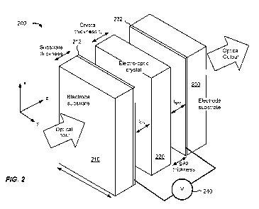
[0012] FIG. 2 is a simplified perspective view of an electro-optic device
according to an
embodiment of the present invention;
[0013] FIG. 3 is a simplified side view of a Pockels cell according to an
embodiment of the
present invention including a flowing coolant;
[0014] FIG. 4 is a simplified side view of a Pockels cell according to an
embodiment of the
present invention including an external flowing coolant;
[0015] FIG. 5 is a simplified side view of a Pockels cell according to an
embodiment of the
present invention including lateral conduction;
[0016] FIG. 6 is a simplified side view of a Pockels cell including anti-
reflection coatings
according to an embodiment of the present invention;
[0017] FIG. 7 is a simplified side view of a set of Pockels cells including
birefringence
compensation according to an embodiment of the present invention;
[0018] FIG. 8 is a simplified side view of a reflective switch according to an
embodiment
of the present invention; and
[0019] FIG. 9 is a simplified flowchart illustrating a method of operating a
Pockels cell
according to an embodiment of the present invention.
DETAILED DESCRIPTION OF SPECIFIC EMBODIMENTS
[0020] According to embodiments of the present invention, optical switches are
provided in
the form of Pockels cells with longitudinal electrode geometries. According to
some
embodiments of the present invention, the drive voltage is independent of
crystal thickness
and the crystal is isotropic in the aperture plane. As described below, the
electrodes used to
apply the electrode field overlap with the optical aperture, and therefore are
transparent or
semi-transparent to permit optical propagation.
[0021] Pockels cells with ring electrodes leave a portion of the crystal
surface unexposed,
but use a thicker crystal (i.e., a higher thickness: aperture ratio) in order
to achieve a
longitudinal electric field with reduced fringing effects. Accordingly, this
design results in
increased absorption and thermal birefringence. As a result, it is difficult
to scale ring
electrode devices to large aperture. Longitudinal devices with plasma (low
pressure gas
phase) electrodes have been constructed, but rely on intimate contact between
the plasma and
the electro-optic crystal. The plasma prevents heat-sinking the aperture faces
of the electro-
4
CA 02815068 2013-04-17
WO 2012/058123
PCT/US2011/057383
optic crystal, which renders the device more susceptible to thermal issues
arising from
residual optical absorption of high power laser light within the crystal. The
plasma electrodes
also increase the complexity of the device, which impacts its cost and
robustness due the
required gas handling system, potential for vacuum system leaks, and potential
electrode
issues such as plasma erosion and arcing.
[0022] Embodiments of the present invention utilize a transparent, conductive
solid as the
electrode in a longitudinal configuration. Transparent, as used herein,
includes low
absorption materials that are less than 100% transmissive. Therefore,
transparent is not
intended to denote 100% transmission, but a high transmission at wavelengths
of interest, for
example, higher than 80%, higher than 85%, higher than 90%, higher than 95%,
higher than
96%, higher than 97%, higher than 98%, or higher than 99%. Transparent
electrodes of
sufficient optical transmission can be fabricated using coating processes of
various types
(e.g., chemical vapor deposition, sputtering, evaporation, electron beam
deposition, spray
coating, or the like), based on extremely thin metal layers or transparent,
conductive oxides
(TC0s) using materials such as indium oxide, tin oxide, indium tin oxide
(ITO), other
transparent, conductive materials, or the like. TCOs are widely used in
devices for displays
and photovoltaic cells.
[0023] The inventors have determined that transparent electrodes exhibit a non-
zero optical
absorption. This residual absorption makes the electrode susceptible to
optical damage
associated with short optical pulses. For example, pulse absorption creates a
transient
thermal stress which can cause coating failure. Furthermore, electrode
absorption increases
with coating thickness, while electrode series resistance (sheet resistance)
increases with
reduced coating thickness. There is thus a tradeoff between switching speed
and optical
damage resistance in the electrode coatings. To date, a suitable coating with
both high
optical damage resistance (coating absorption below ¨1%) and low sheet
resistance (-100
ohms/square) has not been realized on DKDP. Most TCO coating processes have
been
developed for glass substrates, e.g.; for use in commercial applications such
as displays, and
employ high temperatures (-300 C substrate temperature during deposition
and/or during a
post-deposition anneal) to improve the transparency-resistance tradeoff. While
glass
substrates are compatible with such high temperature processes, electro-optic
crystals are
generally not well-suited for such high temperature processes. For example,
DKDP crystals
undergo a destructive phase transition at 145 C. Thus, efforts to coat ITO
directly on
electro-optic crystal such as KDP and DKDP have resulted in electrodes with
either low
damage threshold or high series resistance.
5
CA 02815068 2013-04-17
WO 2012/058123
PCT/US2011/057383
[0024] FIG. 2 is a simplified perspective view of an electro-optic device
according to an
embodiment of the present invention. An exemplary electro-optic device that
alters the
polarization state of an optical input due to application of an applied
voltage is a Pockels cell.
Throughout this specification, a Pockels cell will be discussed as an example
of an electro-
optic device provided by embodiments of the present invention, however, the
present
invention is not limited to Pockels cell implementations. Other electro-optic
devices are
included within the scope of the present invention.
[0025] In one implementation, a Pockels Cell electrode is formed by depositing
a
transparent, conductive solid coating (i.e., an electrode film) on a
transparent optical
substrate, not on the electro-optic crystal, and positioning the coated
substrate in close
proximity to an electro-optic crystal in a longitudinal geometry. Voltage is
applied to the
electrode films to produce an electric field across the electro-optic crystal.
The coating-to-
crystal gap is maintained at a small distance in some embodiments to reduce or
minimize
capacitive voltage drops and therefore switching voltage. Embodiments of the
present
invention provide numerous advantages including, enabling the substrate for
the transparent,
conductive coating to be optimized independently from selection of the electro-
optic crystal.
The substrate can be selected to improve transient cooling of the coating
(better thermal
conductivity and volumetric heat capacity), reduced coating theimal stress
(expansion
coefficient matched to coating), and compatibility with high temperature
processing (to
enable coating annealing that improves resistance and transparency). Another
advantage is
that by appropriate substrate selection, a high transparency (high optical
damage threshold),
low resistance electrode can be realized in a non-plasma design.
[0026] Additionally, the gap between electrode and crystal can be filled with
a transparent,
thermally conductive medium to provide face cooling of the crystal. Face
cooling is
preferred in some embodiments because it reduces thermal birefringence effects
in
comparison with some edge cooling techniques. It should be noted that anti-
reflection (AR)
coatings are not illustrated in FIG. 2 for purposes of clarity. As described
more fully
throughout the present specification, AR coatings can be applied to one or
more surfaces of
the optical elements to improve performance. One of ordinary skill in the art
would
recognize many variations, modifications, and alternatives.
[0027] According to an embodiment of the present invention, an electro-optic
device that
alters the polarization state of an optical input due to application of an
applied voltage is
provided. The electro-optic device includes an electro-optic crystal 220 and a
pair of
electrode substrates 210/230 (one on each side of the crystal in the
embodiment illustrated in
6
CA 02815068 2013-04-17
WO 2012/058123
PCT/US2011/057383
FIG. 2). Each of the electrode substrates, also referred to as electrodes,
includes a
transparent, electrically conductive coating 212/232 on one or more of the
surfaces of the
electrode substrates. The electrode substrates are separated from the electro-
optic crystal by
gaps having predetermined thicknesses, which can support a transparent coolant
material
within the gaps. In one embodiment, the electrodes are pressed directly
against the electro-
optic crystal, reducing the gap dimension to essentially zero. In an
embodiment, the optical
input propagates along a direction perpendicular to the faces of the electro-
optic crystal and
the conductively coated electrode surfaces are oriented parallel to both the
crystal faces and
the optical aperture. Thus, the device operates in transmission mode.
[0028] Referring to FIG. 2, the electro-optic crystal 220 illustrated in the
figure comprises
deuterated potassium dihydrogen phosphate (DKDP) with a predeteimined
thickness tx.
According to embodiments of the present invention, the thickness of the
electro-optic crystal
(e.g., DKDP) ranges from about tx=3 mm to about tx=30 mm, for example, tx=5
mm. Thinner
crystals (e.g., 5 mm in thickness) are suitable for use in the Pockels cell
discussed herein
since thinner crystals reduce or minimize thermal birefringence effects due to
lower
integrated crystal absorption. Crystals thinner than 5 mm are included within
the scope of the
present invention, providing reduced adverse effects and mechanical
robustness. As
discussed in relation to FIG. 3, for embodiments utilizing gas-based coolants
in the electrode
gap, the electro-optic crystal thickness tx is provided at a sufficient
thickness such that the
electric field within the gap remains below the dielectric breakdown electric
field EBR of the
gap coolant:
EGAp = 8' VSWITCH/tx < EBR,
where e is the dielectric constant of the electro-optic crystal, VSWITCH is
the switching voltage
(e.g., either the crystal half-wave or quarter-wave voltage, depending on the
desired degree of
polarization rotation). For example, for a 10 mm thick DKDP crystal operated
at a half-wave
voltage, the gap field is 307 kV/cm. Accordingly, typical gap thickness values
oft 1 mm
are appropriate for He:SF6 gas coolant. As described throughout the present
specification, in
other embodiments, the gap thickness is reduced to several mils (e.g., 25-50
[tm) or less.
Thus, a range of gap thicknesses, from several microns to tens of millimeters
are included
within the scope of the present invention.
[0029] Although the electro-optic device illustrated in FIG. 2 utilizes a DKDP
crystal, other
solids exhibiting an electro-optic effect and good optical transparency are
suitable for use in
other embodiments. For example, other suitable electro-optic crystals include,
without
7
CA 02815068 2013-04-17
WO 2012/058123
PCT/US2011/057383
limitation, undeuterated KDP, lithium niobate, potassium titanyl phosphate
(KTP), rubidium
titanyl phosphate (RTP), rubidium titanyl arsenate (RTA), beta barium borate
(BBO), or the
like. Additionally, although the electro-optic device illustrated in FIG. 2
utilizes two
electrode substrates, this particular implementation is not required by
embodiments of the
[0030] The electrode substrates 210/230 (also referred to as substrates) can
be made of any
suitable material that provides for high optical transmission, mechanical
rigidity, and a
substrate appropriate for formation of the electrode coatings 212/232. As an
example, the
electrode substrates can be sapphire substrates, for example, 1 mm in
thickness. Sapphire is
[0031] Alternative substrate materials include, without limitation, zinc
selenide, zinc oxide,
30 replace an extra wave plate in the optical system and thereby reduce the
number of optical
elements utilized. The electrode substrate can thus serve a dual function as a
suitable
substrate surface for formation of the electrode coating as well as a wave
plate. As
appropriate for wave plate applications, the electrode substrate may actually
be multiple
plates that are bonded together to provide the wave plate functionality.
8
CA 02815068 2013-04-17
WO 2012/058123
PCT/US2011/057383
[0032] Referring once again to FIG. 2, a transparent, conductive electrode
coating 212/232
(also referred to as an electrode coating or a transparent, conductive
electrode thin film) is
provided on one or more surfaces of the electrode substrates 210/230. In an
embodiment, the
electrode coating is fabricated using Indium Tin Oxide (e.g., 10% to 20% tin
in In203) (ITO)
with a thickness ranging from about 5 nm to about 50 nm. The coating thickness
can be
adjusted depending on the particular application to optimize the tradeoff
between coating
transparency and electrical resistance. As an example, the ITO can be
deposited on a
substrate held at a temperature above 100 C during the coating process and
annealed at a
temperature above 100 C after the coating process.
[0033] In the embodiment illustrated in FIG. 2, the electrode coatings are
oriented so that
the coated electrode surfaces face the electro-optic crystal 220. This
orientation provides
benefits, including reductions in the capacitive voltage drop (i.e., no
voltage drop across the
substrates) and thus the switching voltage. An alternative orientation is to
orient the
electrode coatings with the coated surfaces facing away from the electro-optic
crystal. This
will typically increase the switching voltage, but simplify, in some
configurations, the
fabrication of the electrical contact between the conductive coated surface
and external power
supplies.
[0034] Alternative coating materials include any transparent conductive oxide
(such as
Indium Oxide, Tin Oxide, Zirconium Oxide, Zinc Oxide, or the like), any thin
metal coating
(such as gold, silver, aluminum, or the like), transparent conductive polymers
used in organic
light emitting diode (OLED) devices, or other suitable transparent conductive
coatings. One
of ordinary skill in the art would recognize many variations, modifications,
and alternatives.
[0035] The electrode coating can be deposited by any of a variety of
techniques, including
sputtering, reactive sputtering in a partial pressure of 02 for TC05), thermal
evaporation, e-
beam evaporation, ion beam assisted deposition, chemical vapor deposition, dip
coating,
spray coating, or the like. In some implementations, an adhesion layer, for
example, Cr or Ti,
is provided between the electrode material and the substrate. In other
embodiments, a hard
coating such as Hf02, a silicate layer, or the like, can be deposited on the
substrate prior to
the formation of the electrode coating to serve as a buffer layer, an
impedance matching
layer, or the like. Thus, formation of the electrode coating directly on the
electrode substrate
is not required by embodiments of the present invention but is discussed
merely by way of
example.
9
CA 02815068 2013-04-17
WO 2012/058123
PCT/US2011/057383
[0036] The substrate temperature and conditions during coating and any post-
deposition
annealing (e.g., temperature, ambient gas(es), inert gas(es), pressure, and
the like) can be
optimized to achieve the desired transparency and electrical resistance for
the electrode
coating. Typical temperatures during deposition and/or annealing can be near
300 C. A
typical annealing gas used for the deposition of ITO is 10% 02 in an inert gas
such as Ar or
N2. In contrast with attempts to deposit transparent conductive coatings on
electro-optic
crystals, the electrode substrates utilized herein are suitable for high
temperature processing,
enabling the formation (e.g., by deposition) of transparent conductive
coatings with both high
transparency and high conductivity.
[0037] The gap between each electrode coating and the electro-optic crystal
typically
ranges from about 0 mm to about 1 mm. In a particular embodiment, the gap is
0.5 mm. As
described throughout the present specification, the gap will vary depending on
application,
with smaller gaps associated with stagnant coolants and larger gaps associated
with flowing
coolants. In some implementations, the gap is made as thin as possible to
minimize the
switching voltage, consistent with mechanical stability, robustness, and
uniformity
constraints. The switching voltage is given by:
VswITCH= (V/r11) { 1 + 2 (tGAp/eGAp) / (tx/ E'x) 1
where Vit is the crystal half-wave voltage, tx is the thickness of the electro-
optic crystal, tGAp
is the gap thicknesses, six is the dielectric constant of the electro-optic
crystal, and eGAp is the
dielectric constant of the material in the gap. The integer m describes the
switching
configuration (m = 1 for half-wave, m = 2 for quarter-wave). In some
implementations, the
gap thickness is adjusted to minimize the impact of gap variations on optical
transmission
uniformity across the aperture. In some embodiments, switching voltages on the
order of 20
to 30 kV are provided with switching times on the order of 100 to 150 ns. In a
particular
design, a switching time on the order of 50 ns is achieved. Other switching
voltages and
switching times are included within the scope of the present invention.
[0038] The local crystal polarization rotation depends on the local electric
field in the
crystal. If the gap dimension is not constant across the aperture of the
device, then the output
polarization can be nonunifolin. When placed between polarizers, this
nonuniformity can
result in a lateral nonuniformity of the optical intensity profile. For
example, for a half-wave
switch based on highly deuterated KDP (V7,/m = 6.4 kV, six = 48, tx = 25 mm)
with a tGAP =
CA 02815068 2013-04-17
WO 2012/058123
PCT/US2011/057383
0.2 mm gap (E'GAp = 1), a 10 [tm variation in gap dimension changes the
crystal voltage by
136 V. This changes the local optical intensity by 0.45%.
[0039] Gap thickness variations can result from mechanical assembly
imperfections,
vibrations, and pressure differences across the electrodes (due to use of high
pressure coolant)
that cause bowing. For designs that employ flowing coolant, the gap thickness
is provided at
an appropriate width so that the pressure drop due to flow across the crystal
is sufficiently
low. In some implementations, the pressure drop results in a gap thicknesses
of
approximately 0.1 mm for high-pressure flowing gas (e.g., 2-5 atm) and 0.4 mm
for flowing
liquid.
[0040] As discussed above, in one embodiment, the gap thickness is reduced to
essentially
zero. This can be accomplished by several methods, including mechanically
pressing the
electrode to the electro-optic crystal (a technique referred to as "dry
contact"). The dry
contact method benefits from extreme attention to cleanliness of the
contacting surfaces in
order to avoid creation of defects susceptible to laser induced damage.
Another method is
"direct bonding" of the electrode and crystal surfaces (sometimes referred to
as "diffusion
bonding," "adhesive free bonding," or "wafer bonding"). This process may
include coating of
these surfaces with an Si02-based material, for example solgel materials that
can be
employed in AR coatings. Use of a solgel material may provide a coupling layer
between the
electrode substrate and the electro-optic crystal, so that the gap is non-
zero, but direct
physical contact is provided between the electrode substrate and the electro-
optic crystal. An
inorganic fluid may be used in these applications in place of a solgel. Yet
another method is
bonding with a transparent adhesive. This method utilizes an adhesive that can
withstand
high optical fluence and power. Other methods of reducing the gap thickness to
substantially
zero are included within the scope of the present invention and these methods
are provided
merely by way of example. One of ordinary skill in the art would recognize
many variations,
modifications, and alternatives.
[0041] A flowing or stagnant "coolant" material can be provided within the gap
region
between the electrode substrates and the electro-optic crystal in order to
facilitate cooling of
the electro-optic crystal. This coolant can include a transparent gas, liquid,
or the like. In
one implementation, SF6 gas is used at 2.5 atm pressure, whereas in another
implementation,
a 1:1 mixture of SF6:He (by volume) at 5 atm is utilized. A stagnant coolant
design can use a
gas containing at least 2.5 atm partial pressure of SF6 or other appropriate
gas to prevent
dielectric breakdown. The addition of helium to the gas improves the thermal
conductivity of
the cooling gas. The composition of the gas coolant can also include a partial
pressure of
11
CA 02815068 2013-04-17
WO 2012/058123
PCT/US2011/057383
oxygen in order to inhibit chemical decomposition of TCOs at high laser
fluence or power.
The flow of the coolant may be provided in a pulsed format in which the
coolant flows
through the device during laser shots, providing a stagnant fluid during the
shot and then
removing heat using the flowing coolant between shots. Thus, the incorporation
of flowing
coolants into embodiments of the present invention includes implementations in
which the
coolant has a non-zero flow rate at some time during a given period.
[0042] In an implementation using a cooling liquid, fluorinated decalin
(decahydronaphthalene) is provided in the gap region. The purpose of the
"coolant" can be to
provide a theimal conduction path between the crystal faces and the electrodes
(assuming
- external cooling of the electrode faces), to provide direct heat removal by
flowing over the
crystal faces, or other cooling functions. As discussed in relation to the
transparent
electrodes, transparency of the coolant material does not require 100%
transmission, but a
high transmission value.
[0043] In embodiments in which the device is externally cooled by face cooling
the
substrate faces in an external, flowing fluid, the substrate thickness is
typically as thin as
possible (to provide low thermal resistance) consistent with mechanical
strength. Mechanical
strength requirements are impacted by any pressure differential between the
gap "coolant"
and the medium external to the substrate.
[0044] As discussed above, liquids, gases, and combinations thereof, can be
used as
coolants. Liquids can be used as stagnant or flowing coolants. A benefit
provided by
flowing coolant liquids is that carbonized byproducts resulting from high
optical fluence can
be continuously filtered from the liquid to prevent permanent optical
degradation. Flowing
coolants can use the same gas as indicated above for stagnant coolants, or can
use a
transparent liquid that is resistant to optical damage. As will be evident to
one of skill in the
art, device cooling can include heat transfer to flowing fluids that are then
cooled (and may
be filtered) external to the device. These cooling designs can provide face
cooling, which
reduces or minimizes thermal birefringence effects.
[0045] As illustrated in FIG. 2, the electrode substrates and the electro-
optic crystal are
disposed along an optical path extending from the optical input to the optical
output. In an
embodiment, the centers of the various optical elements are disposed along the
optical path to
form a single optical system including the various illustrated optical
elements. Thus, in this
embodiment, the electrode substrates are adjacent the electro-optic crystal on
opposite sides
of the electro-optic crystal and the input and output surfaces of the
electrode substrates and
12
CA 02815068 2013-04-17
WO 2012/058123
PCT/US2011/057383
the electro-optic crystal are parallel. In other embodiments, the input and
output surfaces are
generally parallel but tilted to reduce reflections. It should be noted that
parallel surfaces are
not required for this invention. As an example, the electrode and electro-
optic crystal
surfaces can be curved and provide a constant gas across the curved surfaces.
Thus, the use
of parallel in this description is not intended to require plane parallel. One
of ordinary skill in
the art would recognize many variations, modifications, and alternatives.
[0046] FIG. 3 is a simplified side view of a Pockels cell according to an
embodiment of the
present invention including a flowing coolant. Although FIGS. 3-7 discuss
embodiments of
the present invention used as Pockels cells, the implementations are not
limited to use as
Pockels cells and other electro-optic devices are included within the scope of
the present
invention. Thus, the discussion of Pockels cells is merely provided to provide
exemplary
embodiments in which the various aspects of the present invention can be
illustrated. When
the coolant within the gap region is flowing as illustrated in FIG. 3, the
coolant can be used
for device cooling as described above. The flowing coolant can be externally
filtered to
prevent buildup of particles and contaminants formed by laser-induced coolant
degradation,
which could limit reliability under high energy or high power operation. For
purposes of
clarity in FIG. 3, AR coatings are not illustrated, but can be utilized.
[0047] Electrode substrates 310/330 include electrode coatings 312/332. A
voltage can be
applied across the electro-optic crystal 320. Although the gaps between the
electrode
coatings and the electro-optic crystal are illustrated as equal in thickness,
this is not required
by embodiments of the present invention.
[0048] FIG. 4 is a simplified side view of a Pockels cell according to an
embodiment of the
present invention including an external flowing coolant. In the embodiment
illustrated in
FIG. 4, the coolant within the electrode gap is stagnant and external cooling
is utilized to
transfer heat from the stagnant coolant to an external heat sink (not shown).
In the
embodiment illustrated in FIG. 4, separate coolant flowing over the exterior
surfaces of the
electrode substrate is provided along with an exterior pair of windows to
contain this flowing
coolant. In one implementation, the flowing coolant (i.e., exterior coolant)
includes high
pressure helium gas. Since the flowing coolant is not disposed in a high
electric field, SF6 is
not required to prevent electrical breakdown. In addition to flowing gas
coolants, flowing
liquid coolants can also be used. For purposes of clarity in FIG. 4, AR
coatings are not
illustrated, but can be utilized.
13
CA 02815068 2013-04-17
WO 2012/058123
PCT/US2011/057383
[0049] The exterior windows illustrated in FIG. 4 can be any transparent
material resistant
to optical damage, such as fused silica or sapphire. The thickness of the
exterior windows is
selected to avoid polarization distortions due to stress birefringence
associated with pressure
-
differentials.
[0050] FIG. 5 is a simplified side view of a Pockels cell according to an
embodiment of the
present invention including lateral conduction. The alternative design
illustrated in FIG. 5
provides conductive cooling of the device by heat sinking the edges of the
electrode
substrates (i.e., lateral conduction through the electrode substrate). This
approach utilizes
electrode substrates with sufficient thermal conductivity, such as sapphire,
ZnO, ZnS, or the
like. Although glass or silica substrates are less suitable for this
implementation, they can be
used as electrode substrates as well.
[0051] FIG. 6 is a simplified side view of a Pockels cell including anti-
reflection coatings
according to an embodiment of the present invention. In typical
implementations, all
appropriate surfaces of this device will be AR coated, as shown, for example,
in FIG. 6.
Appropriate surfaces for AR coats include: both surfaces of the electro-optic
crystal
(644/646); both surfaces of both electrode substrates (640/642 and 648/650);
and the surfaces
of any exterior windows used to confine additional cooling fluids. The AR
coatings can be
applied on top of the conductive coating (i.e., the layer stack is electrode
substrate /
conductive coating (620/622) / AR coating (642/648) in the illustrated
implementation.
Depending on the particular application, one or more of these surfaces can be
AR coated to
improve optical transmission through the electro-optic device. Depending on
the particular
application, one or more of these surfaces can be tilted to reduce or minimize
optical etalon
effects. Thus, although all surfaces are coated in the implementation
illustrated in FIG. 6,
this is not required by the present invention. As an example, in some
implementations using
flowing liquid coolant, the liquid coolant may provide an index matching
function, reducing
or eliminating the need for an AR coating on the electro-optic crystal and the
electrode
coating. Thus, some surfaces may not be AR coated depending on the
implementation. One
of ordinary skill in the art would recognize many variations, modifications,
and alternatives.
[0052] FIG. 7 is a simplified side view of a set of Pockels cells including
birefringence
compensation according to an embodiment of the present invention. For certain
cooling
geometries, or for very high optical power, the electro-optic device may
exhibit a residual
theiinal birefringence that is undesirable. In this case, the thermal
birefringence can be
compensated using two electro-optic devices in series with an optical rotator
crystal placed
between them as shown in FIG. 7. The optical rotator can be realized with a
chiral (optically
14
CA 02815068 2013-04-17
WO 2012/058123
PCT/US2011/057383
active) crystal such as quartz or potassium dithionate. For operation at 1 p.m
wavelength, a
quartz rotator will be approximately 13.7 mm thick. The rotator crystal will
typically be AR
coated. Alternatively, the optical rotator can use a Faraday rotator material
in a magnetic
field. Suitable Faraday rotator crystals include terbium gallium garnet,
certain doped glasses,
and the like.
[0053] In the embodiment illustrated in FIG. 7, it is desirable to use electro-
optic crystals
with identical or nearly identical thickness. Since the birefringence being
compensated is
much less than that of the transverse electrode configuration, the tolerance
for thickness
matching is significantly relaxed from the transverse configuration. For
example, a 25 mm
thick crystal of highly deuterated (98%) KDP will exhibit a theinial
birefringence of 3.6 x 10-
4 and will require thickness matching to no better than 0.26 mm. For purposes
of clarity in
FIG. 7, AR coatings are not illustrated, but can be utilized.
[0054] An alternative approach to compensate excessive themial birefringence
is to
separately heat the periphery of the electro-optic crystal. This could be
accomplished, for
example, with resistive heaters, by illumination from an additional optical
source, or other
suitable technique.
[0055] FIG. 8 is a simplified side view of a reflective switch according to an
embodiment
of the present invention. In this implementation, the same electrode approach
described
above for a transmission mode device is applied to a reflection mode device.
As illustrated in
the figure, the single electrode is used in the form of a gap-coupled
electrode substrate 810
including a transparent substrate having one face coated with a transparent,
electrically
conductive thin film 820. A metal heat sink 860 can be used to provide heat
sinking. A
coolant within the gap is optional in the illustrated embodiment. As a variant
on the design
illustrated in FIG. 8, the metal block can be coated with a high-reflection
(HR) coating 850 to
improve both the optical throughput and optical damage threshold of the
electro-optic device.
Application of a voltage across the electro-optic crystal will enable the
polarization of the
input light to be modified, providing a switching function. AR coatings
840/842/844 are
illustrated. One of ordinary skill in the art would recognize many variations,
modifications,
and alternatives.
[0056] According to an embodiment of the present invention, a reflective
electro-optic
device is provided. The reflective electro-optic device comprises an electrode
substrate
having an input surface and an output surface and an electrode coating coupled
to the output
surface. The reflective electro-optic device also includes an electro-optic
crystal having a
CA 02815068 2013-04-17
WO 2012/058123
PCT/US2011/057383
first surface and a second surface. The first surface of the electro-optic
crystal is separated
from the electrode coating by a gap having a predetermined thickness. An HR
coating is
coupled to the second surface of the electro-optic crystal. The electro-optic
crystal is
mounted to a heat sink thermally coupled to the second surface of the electro-
optic crystal.
Light incident on the input surface of the electrode substrate passes through
electrode
substrate, the electrode coating, which is transparent, the gap, and the
electro-optic crystal.
The light is then reflected by the HR coating and passes back through the
above structures as
illustrated in FIG. 8.
[0057] FIG. 9 is a simplified flowchart illustrating a method of operating a
Pockels cell
according to an embodiment of the present invention. The method includes
providing a
Pockels cell (910) having a first electrode substrate having an input surface,
an output
surface, and a first electrode coating coupled to the output surface. The
Pockels cell also has
an electro-optic crystal disposed adjacent to the first electrode substrate
and a second
electrode substrate having an input surface, an output surface, and a second
electrode coating
coupled to the input surface. As an example, the electro-optic crystal can be
DKDP. As
discussed throughout the present specification, the first electrode coating
can include ITO and
the second electrode coating can include ITO. The method also includes
directing an input
beam having a first polarization state to impinge on the input surface of the
first electrode
substrate (912), passing at least a portion of the input beam through the
first electrode
substrate (914), and passing at least a portion of the input beam through the
first electrode
coating (916).
[0058] The method further includes applying a voltage between the first
electrode coating
and the second electrode coating (918) and changing the first polarization
state into a second
polarization state using the electro-optic crystal (920). In some embodiments,
the change in
polarization state is associated with a phase difference between the second
polarization state
and the first polarization state of a half-wave, whereas in other embodiments,
the change in
polarization state is associated with a phase difference between the second
polarization state
and the first polarization state of a quarter-wave. Thus, the Pockels cell is
able to function as
a half-wave plate, a quarter-wave plate, or the like. During operation, the
Pockels cell can
convert light in a linear polarization state to a circular polarization state,
an elliptical
polarization state, or the like. Additionally, the method includes passing at
least a portion of
the input beam through the second electrode coating (922) and passing at least
a portion of
the input beam through the second electrode substrate (924).
16
CA 02815068 2013-04-17
WO 2012/058123
PCT/US2011/057383
[0059] It should be appreciated that the specific steps illustrated in FIG. 9
provide a
particular method of operating a Pockels cell according to an embodiment of
the present
invention. Other sequences of steps may also be performed according to
alternative
embodiments. For example, alternative embodiments of the present invention may
perform
conducting thin film have been simulated. Changes due to optimization of the
thin film's
substrate were investigated. The properties of the film and substrate are
shown in Table 1.
Typical values were selected for the ITO optical absorption for annealed and
unannealed
films of thickness of 100 nm.
Thermal Heat Thermal Young's
Optical
Material Conductivity Capacity Density Expansion Modulus
Absorption
W/m-K J/kg-K kg/cm3 ppm/K GPa
ITO (unannealed) 3.2 365 7140 7.25 170 5%
ITO (annealed) 3.2 365 7150 7.25 170 2%
DKDP 1.4 857 2355.5 24.90
Sapphire 42.0 761 3980 7.00
Fused Silica 1.4 740 2200 0.55
Table 1
[0061] The thermomechanical shock due to laser-induced heating of the coating
was
simulated using a transient, 1-dimensional thermal solver using temperature-
independent
[0062] The thermal simulations provide maximum temperatures at the ITO surface
and at
17
CA 02815068 2013-04-17
WO 2012/058123
PCT/US2011/057383
Strain 8= Aa AT
Stress a= E s,
where AT is the temperature rise at the interface, Act is the differential
thermal expansion
between the ITO and substrate, and E is the Young's modulus of the coating.
[0063] Results of the simulations of the laser-induce thermomechanical load
are shown in
Table 2. For unannealed ITO on DKDP, the coating temperatures are quite high.
The
corresponding mechanical stress is extremely high (due to the large expansion
coefficient
mismatch) as compared for example to the 165 MPa flexural strength of ITO.
Annealing is
not feasible on DKDP substrates, due to the destructive phase transition of
DKDP at 145 C.
These results semi-quantitatively explain the low optical damage threshold
achievable for
ITO deposited on DKDP, which result from the high optical absorption (due to
higher
material absorptivity), the poor thenual properties of DKDP, and the large
expansion
coefficient mismatch between ITO and DKDP.
ITO Temperature Rise (K) Interface Loads
Substrate Absorption ITO Surface Interface Stress (MPa) Strain
DKDP 5% 613.7 418.5 1255 7.40E-
03
Fused silica 2% 245.8 173.8 198 1.16E-03
Sapphire 5% 559.8 142.0 6.0 6.50E-05
Sapphire 2% 220.9 56.8 2.4 1.40E-05
Table 2
Table 2 also shows how annealing (which lowers the coating absorption)
improves the
thennomechanical loads to improved levels. Notably, the maximum laser-induced
temperature rise of the ITO is similar to the annealing temperatures typically
used for TCO
films (300-500 C). These results explain the better optical damage resistance
observed for
ITO on glass substrates.
[0064] Finally, simulations indicate that the interface stress of annealed ITO
on silica is
still moderately high (198 MPa). The same films exhibit much lower stress on
sapphire
substrates, because the sapphire provides better thermal transport of heat
away from the
interface due to its high thennal conductivity, as well as a closer expansion
coefficient match
to the ITO. These results imply that ITO will be significantly more robust
(80x lower
interface strain) to laser-induced heating when deposited on a sapphire
substrate.
18
CA 02815068 2013-04-17
WO 2012/058123
PCT/US2011/057383
[0065] The following provide device designs and performance calculations
related to
embodiments of the present invention. Designs assume a 25 x 25 cm2 aperture
and utilize a
highly deuterated, z-cut DICDP crystal. The DKDP properties used for
calculations are:
Absorption coefficient, z: 0.25%/cm
Dielectric constant, z: 48
Half-wave Voltage: 6.4 kV
Thernial conductivity, z: 1.2 W/m-K
Thermal conductivity, xy: 1.4 W/m-K
Temperature coefficient of ln V7, = d in V7,/dT: 0.0132/K
Curie Temperature: 222 K
Curie Constant: 3572 K
Thermal expansion, z: 44 ppm/K
Thelmal expansion, xy: 24.9 ppm/K
Mechanical stiffness tensor Cd: from Landolt Bornstein
The ITO coating absorption was assumed to be 2% per electrode.
[0066] Designs were evaluated assuming an optical beam of fluence of 0.345
J/cm2 and
repetition rate 16 Hz. This corresponds to a pulse energy of 215.6 J and
average power 3.45
kW incident on the Pockels Cell.
[0067] The simulation methodology used analytic formulae for the switching
voltage and
device capacitance (plane parallel capacitor approximation with fringing
fields neglected), for
the internal crystal temperature variation, and for the caloric rise of
flowing coolant. An
analytic series expansion was used for mechanical plate deformations (bowing)
due to
pressure differentials.
[0068] The pressure drop due to fluid flow was calculated using the Petukhov
correlation
for smooth channels for turbulent flow, and using the Darcy formula for
laminar flow.
Convective heat transfer across flowing fluid boundary layers was calculated
using the
Gnielinski correlation for turbulent flows and a uniform temperature
correlation for laminar
flow. These results assume smooth channels, fully developed flows, and ignore
pressure
drops associated with transitions to and from the channels.
19
CA 02815068 2013-04-17
WO 2012/058123
PCT/US2011/057383
[0069] The loss due to optical scattering in turbulent gas flows was estimated
using
correlations determined from experimental data, for example, results were
obtained for N2,
and were scaled to other gases using the ratio of Gladstone-Dale coefficients.
[0070] The extinction ratio degradation in the "off' state (no applied
voltage) is degraded in
some embodiments by theunal birefringence, which causes a small fraction of
light to leak
through the switch. This leakage was estimated from finite element
calculations of the
temperature distribution and its resulting strain distribution in the DKDP due
to laser-induced
heating (crystal absorption). These calculations used the anisotropic theunal
and mechanical
properties of the crystal. The strain distribution was mapped to birefringence
using the
founula:
8n= n3 p66 Exy,
where p is the strain-optic coefficient.
[0071] It is reported in our detailed results as the isolation, or inverse
extinction ratio,
which is 0.0 for an ideal device, and given by
sin2 21-c on La,
with finite thermal birefringence. While devices that are face-cooled should
ideally exhibit
no thermal birefringence, even with a linear transverse temperature gradient
due to coolant
caloric rise, the finite extent of the laser beam generally creates a finite
birefringence due to
transverse theunal diffusion at the edge of the laser beam.
[0072] The calculated extinction ratio degradation due to birefringence
includes only
thermal birefringence. It does not include the stress birefringence of windows
and substrates
subjected to pressure differentials; these effects can be mitigated, if
necessary, by increasing
the thickness of the mechanically stressed materials.
[0073] In the "on" state (nonzero applied voltage), lateral variations in the
optical output
polarization (and intensity after traversing a polarizer) can be induced by
bowing of the
electrode and theunal variations across the crystal. Bowing effects were
estimate using
parallel plate capacitor formulas for the local field in the crystal.
Temperature effects were
estimated from the temperature coefficient of V,, and the temperature
variation of the DKDP
dielectric constant (Curie law).
CA 02815068 2013-04-17
WO 2012/058123
PCT/US2011/057383
[0074] The following sections provide the details for four different designs
according to
embodiments of the present invention. In all cases, the following design
constraints were
met:
[0075] The DKDP crystal thickness was always constrained to ensure that the
internal
longitudinal temperature variation (along z in Fig. 1) was < 1 C. This
maintains the internal
stress within the crystal to less than 6% of the fracture limit.
[0076] The combination of DKDP thickness, gas composition, and gas pressure
was always
adjusted so that electric fields within the gas were always 1.8x less than the
dielectric
breakdown field of the gas.
[0077] The gap thickness was always at least 25 microns.
[0078] The pressure drop of flowing coolant never exceeded 1 psi.
[0079] The thickness of windows and substrates was always sufficient to
provide at least
1.5x safety margin against fracture due to pressure differences across these
materials.
[0080] The coolant inlet temperature to the device was 300 K, to avoid the
need for
refrigeration.
[0081] The four exemplary designs can be summarized as follows:
[0082] Typical designs require half-wave switching voltages of 21 to 31 kV.
Certain
designs offer switching voltages as low as 7 to 8 kV; however, these designs
require
maintaining stable gap dimensions of 25 to 50 microns, and are more
susceptible to thermal
birefringence.
[0083] Liquid cooled devices can offer extremely low themial birefringence and
can
employ thin (<8 mm) DKDP crystals and sapphire substrates. The primary concern
with
these devices is long term stability of the liquid coolant at high optical
power and fluence.
[0084] Devices with gas coolants require thick DKDP crystals (25 mm) and high
gas
pressures (5 atm) to avoid gas breakdown. This requires thick substrates or
windows. It also
causes a significant loss of local extinction ratio (1.2%) due to increased
thermal
birefringence. This reduced extinction value is localized to a small area of
the crystal.
[0085] Transversely cooled devices exhibit worse local extinction (>2%).
[0086] Design 1: Face-cooled Design with Flowing Gas Coolant in the Gap
(Reference can
be made to FIG. 3)
21
CA 02815068 2013-04-17
WO 2012/058123
PCT/US2011/057383
[0087] Design Parameters
Crystal thickness: 25 mm
Gap thickness: 1.0 mm
Substrate: c-plane sapphire
Substrate thickness: 20 mm
Coolant: 1:1 He:SF6 by volume, 5 atm pressure
Coolant flow: 18 m/s
[0088] Thermal and Cooling Performance
Caloric rise of coolant: 0.3 C
Crystal internal temperature rise: 0.9 C
Boundary layer temperature rise: 2.6 C (crystal to coolant interface)
Total crystal temperature rise: 3.8 C
Coolant flow pressure drop: 0.5 psi
[0089] Electrical Performance
Half-wave switch voltage: 30.9 kV
Capacitance: 257 pF
[0090] Electro-optic Performance
Optical absorption: 4.6% (KDP plus ITO)
Optical scattering loss: 0.16% (SF6 gas)
Local Extinction degradation 1.22% (thermal birefringence)
Contrast degradations in transmission
Bowing <0.01%
Lateral temperature variation <0.01%
[0091] It should be noted that the electric field in the gap is at a level
1.8x below the
breakdown field of the gas; the switching voltage can be reduced to 23.5 kV by
reducing the
gap to 0.7 mm, changing the coolant flow to 8.4 m/s, and allowing a caloric
rise of 0.6 C.
22
CA 02815068 2013-04-17
WO 2012/058123
PCT/US2011/057383
These changes result in an increased device capacitance of 337 pF; the 2 cm
substrate
thickness provides sufficient fracture resistance and prevents substrate
bowing (localized
switch voltage variations due to the pressurized coolant); a 9.2 cm silica
substrate could be
used in place of the sapphire. However, the damage resistance of the ITO would
likely be
reduced.
[0092] Design 2: Face-cooled Design with Flowing Liquid Coolant in the Gap
(Reference
can be made to FIG. 3)
[0093] Design Parameters
Crystal thickness: 8 mm
Gap thickness: 0.4 mm
Substrate: c-plane sapphire
Substrate thickness: 5 mm
Coolant: fluorinated decalin
Coolant flow: 0.24 m/s
[0094] Thermal and Cooling Performance
Caloric rise of coolant: 0.1 C
Crystal internal temperature rise: 0.1 C
Boundary layer temperature rise: 2.0 C (crystal to coolant interface)
Total crystal temperature rise: 2.2 C
Coolant flow pressure drop: 1.0 psi
[0095] Electrical Perfoimance
Half-wave switch voltage: 20.8 kV
Capacitance: 1194 pF
[0096] Electro-optic Performance
Optical absorption: ' 4.2% (KDP plus ITO)
Optical scattering loss: 0 % (SF6 gas)
Local Extinction degradation 0.02% (theimal birefringence)
23
CA 02815068 2013-04-17
WO 2012/058123
PCT/US2011/057383
Contrast degradations in transmission
Bowing <0.01%
Lateral temperature variation <0.01%
[0097] It should be noted that the liquid coolant can be externally filtered
(micropore) to
remove potential impurities generated by laser-induced degradation.
[0098] Design 3. Face-cooled Design with Flowing Gas Coolant External to the
Substrate
(Reference can be made to FIG. 4)
[0099] Design Parameters
Crystal thickness: 25 mm
Gap thickness: 0.050 mm
Gap material: stagnant 1:1 He:SF6 by volume, 5 atm
pressure
Substrate: c-plane sapphire
Substrate thickness: 1 mm
Window: Fused silica
Window thickness: 10 mm
Coolant: 1:1 He:SF6 by volume, 5 atm pressure
Coolant flow: 25.5 m/s
[0100] Themial and Cooling Perfoitnance
Caloric rise of coolant: 0.4 C
Crystal internal temperature rise: 0.9 C
Boundary layer temperature rise: 4.8 C (crystal to coolant interface)
Total crystal temperature rise: 6.1 C
Coolant flow pressure drop: 0.2 psi
[0101] Electrical Performance
Half-wave switch voltage: 7.6 kV
Capacitance: 1041 pF
24
CA 02815068 2013-04-17
WO 2012/058123
PCT/US2011/057383
[0102] Electro-optic Performance
Optical absorption: 4.6 % (I(DP plus ITO)
Optical scattering loss: 0% (SF6 gas)
Local Extinction degradation TBD, >1.22% (thermal birefringence)
Contrast degradations in transmission
Bowing 0%
Lateral temperature variation <0.01%
[0103] It should be noted that the electric field in the gap is at a level
1.8x below the
breakdown field of the gas; since no turbulent SF6 flow occurs in the coolant,
scattering loss
is essentially zero; since there is no pressure drop across the substrate,
it's thickness is
constrained only by mechanical robustness considerations; since there is no
pressure drop
across the substrate, there is no bowing-induced degradation of the contrast;
to simplify gas
handling, a variant of this design uses the 1:1 He:SF6 mixture for both the
gap and gas and
flowing coolant. This reduces the boundary layer rise to 2.6 C and the total
temperature rise
to 4.1 C. However, it increases the optical scattering loss to 0.03%.
[0104] Design 4. Edge-cooled (conduction cooled) Design with Stagnant Gas in
the Gap
(Reference can be made to FIG. 5)
[0105] Design Parameters
Crystal thickness: 25 mm
Gap thickness: 0.025 mm
Gap material: stagnant 1:1 He:SF6 by volume, 5 atm
pressure
Substrate: c-plane sapphire
Substrate thickness: 23 mm
Flowing coolant: None
[0106] Thennal and Cooling Performance
Transverse temperature variation: 1.8 C (variation across crystal
aperture)
Crystal internal temperature rise: 0.9 C
CA 02815068 2013-04-17
WO 2012/058123
PCT/US2011/057383
Total crystal temperature rise: not calculated
[0107] Electrical Performance
Half-wave switch voltage: 7.0 kV
Capacitance: 1131 pF
[0108] Electro-optic Performance
Optical absorption: 4.6 % (KDP plus ITO)
Optical scattering loss: 0% (SF6 gas)
Local Extinction degradation 2.1% (thermal birefringence)
Contrast degradations in transmission
Bowing 0%
Lateral temperature variation 0.03%
[0109] It should be noted that the electric field in the gap is at a level
1.8x below the
breakdown field of the gas; since no turbulent SF6 flow occurs in the coolant,
scattering loss
is essentially zero.
[0110] It is also understood that the examples and embodiments described
herein are for
illustrative purposes only and that various modifications or changes in light
thereof will be
suggested to persons skilled in the art and are to be included within the
spirit and purview of
this application and scope of the appended claims.
26