Note: Descriptions are shown in the official language in which they were submitted.
CA 02816468 2015-01-15
52398-8
1
Description
HIGH-VOLTAGE SWITCH WITH COOLING DEVICE
The present invention relates to a high-voltage switch with
cooling device and a Pockels cell drive circuit and a laser
beam source.
For switching laser pulses use is made of optical switches or
modulators, which can be arranged either within or outside the laser
resonator in the beam path. In the case of the optical modulators,
a distinction is made, in principle, between electro-optical
modulators and acousto-optical modulators. One important parameter
when using optical modulators is the achievable switching time. In
the case of acousto-optical modulators, the achievable switching
time is limited by the speed of sound and the laser beam diameter,
such that in some cases the switching edges of acousto-optical
modulators are too slow to effectively suppress for example
preceding or succeeding pulses at a short distance from the main
pulse. By contrast, in the recent past, electro-optical modulators
have been developed further in the direction of higher clock rates,
such that they would be able to replace acousto-optical modulators
in specific laser applications, since they are distinguished by
significantly shorter, electronically governed switching edges.
As a result, electro-optical modulators are constructed such that
they comprise a Pockels cell as the actual optical switching element
having variable optical properties and a polarization-selective
element such as, for example, a reflective analyzer having
invariable optical properties. A Pockels cell generally comprises
a birefringent crystal which is aligned in a suitable manner with
an incident monochromatic and polarized light beam and to which an
electrical voltage of the order of magnitude of a few hundred v to
B0029US CA 0281646,8 2013-04-30
2
a few kilovolts is applied. In conjunction with the
polarization-dependent optical element, the Pockels cell can, in
a manner dependent on the electrical voltage applied to it,
(a) switch the light on or off, or
(b) direct the light on two different paths through an optical
system.
By means of a suitable switchable high-voltage supply, the Pockels
cell can be switched back and forth between two states, in which
the laser beam emerging from the Pockels cell is linearly polarized
with polarization directions that are respectively perpendicular
to one another. The voltage required to achieve the two states
respectively mentioned is a function of the crystal parameters and
the used wavelength of the light to be switched. There are
applications of Pockels cells in which the latter have to be
switched on and off rapidly, wherein both transition times have to
be in the range of a few nanoseconds. In some applications, only
one of said transition times has to be short, either the
switching-on or the switching-off, wherein the respective other
transition time can indeed be in the range of microseconds.
Such an electro-optical modulator, constructed from a Pockels cell
and a suitable switchable high-voltage supply, can be used for
example for optically switching short laser pulses having a
duration of a few nanoseconds (ns) or ultrashort laser pulses having
a picosecond (ps) or femtosecond (fs) duration, that is to say for
changing the intensity or the beam direction of the laser pulses.
As is known, such ultrashort laser pulses are generated by the
method of mode locking. Therefore, laser beam sources for
ultrashort pulses fundamentally always have very high repetition
rates (greater than megahertz (MHz), typically 40-200 MHz for
solid-state lasers) and low pulse energies (in the nanojoule range,
typically 0.1-50 nJ). If individual pulses or pulse groups of ps
or fs laser pulses are required, then a Pockels cell is often used
B0029US
CA 02816468 2013-04-30
3
to select these pulses. In this case, firstly, between two pulses,
which the laser beam source typically emits with a temporal spacing
of 5-25 ns, the voltage has to be completely switched on so as to
be completely switched off again after transmission of a single
laser pulse 5-25 ns later.
One general aim is to constantly increase the maximum possible
repetition rate of the Pockels cell in order thus to increase the
rate at which pulses or pulse groups can be selected by the Pockels
cell. The maximum repetition rate of the Pockels cell is essentially
determined by the maximum repetition rate with which the
high-voltage switch that drives the Pockels cell can be operated.
A high-voltage switch according to the disclosure is connected to
a cooling device and comprises one or a plurality of high-voltage
transistors and a cooling substrate, which is produced from an
electrically insulating material and on or through which a cooling
medium can flow, wherein the high-voltage transistor or
high-voltage transistors are mounted on at least one surface of the
cooling substrate.
The high-voltage transistors used can be, in principle, any desired
switchable transistors having any desired dielectric strengths,
e.g. MOSFETs, bipolar transistors, etc. The dielectric strength can
be, for example, 100 V or more, but transistors having dielectric
strengths of 500 V or more are preferably used.
The maximum possible repetition rate of a high-voltage switch is
determined, inter alia, by the maximum possible consumption of
electrical power at the high-voltage switch and the heat that is
correspondingly to be dissipated. To a first approximation, for
this purpose, the following formula holds true:
P = fREp X (a x U2 + b) (1)
B0029US .
CA 02816468 2013-04-30
4
where P is the consumed electrical power, fREE, is the repetition
rate, U is the applied high voltage and a, b are constants.
The high-voltage switch according to the disclosure has the
advantage, then, that a very efficient heat dissipation is made
possible since the heat only has to flow through a wall of the
cooling plate as far as the flowing cooling medium. A further
advantage of the high-voltage switch according to the disclosure
is that, on account of the electrically insulating material of the
cooling plate, no appreciable parasitic capacitances are formed,
and so no losses as a result of charging and discharging of the
capacitances need be feared in this regard.
In the simplest case, the cooling substrate can be by a plate which
is produced from the electrically insulating material and on which
the cooling medium flows. However, one particularly practicable
embodiment consists in the cooling substrate being at least partly
formed by a hollow body, through which the cooling medium flows.
In this case, the walls of the hollow body are produced from the
electrically insulating material and an inlet opening for the
cooling medium is shaped into one wall and an outlet opening for
the cooling medium is shaped into the same or another wall.
In accordance with one embodiment of the high-voltage switch, the
electrically insulating material of the cooling substrate
comprises a ceramic material or consists thereof. In particular,
in this case, the ceramic material comprises the compound aluminum
nitride (A1N) or consists thereof. As is known, the ceramic material
aluminum nitride has a high thermal conductivity of approximately
180 W/mK.
In accordance with one embodiment, the electrically insulating
material of the cooling substrate comprises any other ceramic
B0029US
CA 02816468 2013-04-30
material desired or any desired nonmetallic material or consists
of these materials mentioned, wherein preferably the thermal
conductivity of the ceramic material or of the nonmetallic material
is greater than 50 W/mK, preferably greater than 100 W/mK, or
preferably greater than 150 W/mK.
In accordance with one embodiment of the high-voltage switch, the
high-voltage transistors each have a planar cooling area and are
applied with their cooling area directly areally on the planar
surface of the cooling substrate. In this way, it is possible to
ensure an optimum heat transfer between the high-voltage
transistors, on the one hand, and the cooling substrate, on the
other hand.
In accordance with one embodiment of the high-voltage switch, one
portion of the high-voltage transistors is mounted on a first
surface of the cooling substrate and another, in particular
remaining, portion of the high-voltage transistors is mounted on
a second surface of the cooling substrate, wherein the first surface
and the second surface lie in different planes. The first surface
and the second surface of the cooling substrate can be arranged,
in particular, in a manner situated opposite one another and in
mutually parallel planes. Furthermore, half of the high-voltage
transistors can be mounted on the first surface and the other half
of the high-voltage transistors can be mounted on the second
surface.
In accordance with one embodiment of the high-voltage switch, the
high-voltage transistors are interconnected to form a push-pull
circuit. In this case, first high-voltage transistors can be
connected in series between a first pole of a voltage source and
a node, and the second high-voltage transistors can be connected
in series between a second pole of the voltage source and the node.
In this case, it can be provided that the first high-voltage
B0029US,
CA 02816468 2013-04-30
6
transistors are mounted on a first surface of the cooling substrate
and the second high-voltage transistors are mounted on a second
surface of the cooling substrate and the first surface and the
second surface are situated opposite one another and are arranged
in mutually parallel planes.
In accordance with another embodiment of the high-voltage switch,
the high-voltage transistors are interconnected to form a bridge
circuit, in particular to form a bridge circuit having an H
configuration. In this embodiment, too, it can be provided that the
high-voltage transistors are mounted half each on a first and a
second surface of the cooling substrate.
The described manner of mounting the high-voltage transistors in
equal halves on two opposite sides of the cooling substrate is
particularly advantageous since, firstly, the cooling capacity
= provided is utilized efficiently and, second, a space-saving
arrangement of the high-voltage transistors is made possible.
A high-voltage switch according to the disclosure can furthermore
contain a number of charging/discharging circuits corresponding to
the number of high-voltage transistors, each of which circuits is
connected to one high-voltage transistor of the one or the plurality
of high-voltage transistors. The internal construction of the
charging/discharging circuits is not the subject matter of the
present application. In one exemplary embodiment, the
charging/discharging circuits are likewise applied on the cooling
substrate, wherein each charging/discharging circuit can be
arranged in spatial proximity to the high-voltage transistor
assigned to it. As an alternative thereto, however, the
charging/discharging circuits can also be arranged outside the
cooling substrate, for instance on a circuit board connected to the
cooling substrate.
CA 02816468 2016-04-08
52398-8
7
The present disclosure likewise relates to the use of a high-
voltage switch according to the disclosure in a Pockels cell
drive circuit and to the use of a correspondingly driven
Pockels cell as a pulse selector in conjunction with a laser
beam source. In this case, the Pockels cell can optionally be
arranged in the laser resonator or else outside the laser
resonator.
According to one aspect of the present invention, there is
provided a high-voltage switch with a cooling device,
comprising: a plurality of high-voltage transistors, a cooling
substrate, produced from an electrically insulating material,
and on or through which a cooling medium can flow, wherein
first high-voltage transistors of the plurality of high-voltage
transistors are mounted on a first surface of the cooling
substrate and second high-voltage transistors of the plurality
of high-voltage transistors are mounted on a second surface of
the cooling substrate, wherein the first high-voltage
transistors are electrically coupled with the second high-
voltage transistors, and the first and second surfaces of the
cooling substrate lie in different planes.
According to another aspect of the present invention, there is
provided a high-voltage switch, comprising: a plurality of
high-voltage transistors; and a cooling substrate, produced
from an electrically insulating material, the cooling substrate
comprising a first main surface, a second main surface, and
four side surfaces connecting the first and second main
surfaces; wherein first high-voltage transistors of the
plurality of high-voltage transistors are mounted on the first
main surface of the cooling substrate and second high-voltage
CA 02816468 2016-04-08
52398-8
7a
transistors of the plurality of high-voltage transistors are
mounted on the second main surface of the cooling substrate.
Exemplary embodiments of the disclosure are explained in
greater detail below with reference to the drawings, in which:
Figures 1A, B show an illustration of a high-voltage
switch in accordance with one embodiment in
a lateral cross-sectional view (A) and a
perspective view (B);
Figures 2A, B show an illustration of a high-voltage
switch in accordance with one embodiment in
a lateral cross-sectional view (A) and a
perspective view (B); and
Figure 3 shows a circuit diagram of a high-voltage
switch in the embodiment of a push-pull
circuit.
Insofar as the following description, the patent claims or the
drawings express the fact that circuit elements are
"connected", "electrically connected" or "coupled" to one
another, this can mean that the elements mentioned are coupled
to one another directly, that is to say without further
elements situated in between. However, it can also mean that
the elements mentioned are coupled to one another indirectly
and that further elements are coupled between the elements
mentioned.
Insofar as identical reference signs are used in the figures,
they refer to identical or functionally identical elements, and
so the
BOG29US
CA 02816468 2013-04-30
8
description of these elements is not repeated in these cases.
Figure 1 shows a high-voltage switch in accordance with one
embodiment in a lateral cross-sectional view (A) , and a perspective
view (B) . The high-voltage switch 10 substantially comprises a
cooling substrate 1 and a number of high-voltage transistors 2
arranged on a main surface lA of the cooling substrate 1. The cooling
substrate 1 is embodied in the form of a parallel-epipedal hollow
body and thus has two large main surfaces lA and 1B, longitudinal
side faces 1C and 1D and transverse side faces lE and 1F. The cooling
substrate 1 is produced by the ceramic material aluminum nitride
(A1N) and, as is known, thus has a thermal conductivity of
approximately 180 W/mK.
In a longitudinal side face 1C, the cooling substrate 1 has an inlet
opening 1C.1 and an outlet opening 1C.2, through which a cooling
medium such as, in the simplest case, water can flow into and out
of the interior of the hollow body of the cooling substrate 1 formed
by the walls 1A-1F. It goes without saying that, instead of being
shaped into the longitudinal wall 1C, the inlet and outlet openings
1C.1 and 1C.2 can alternatively also be shaped into a transverse
wall 1E or 1F or else, under certain circumstances, into one of the
walls lA or 1B of the cooling substrate 1. The inlet and outlet
openings can also be shaped into different walls of the cooling
substrate 1. The high-voltage transistors 2 are of identical design
and each have a lower planar cooling area with which they are
directly applied areally on the first main surface 1A of the cooling
substrate 1. The heat produced by the high-voltage transistors 2
owing to the consumption of electrical power thus only has to be
transported through this wall of the highly thermally conductive
ceramic material AIN to the cooling medium.
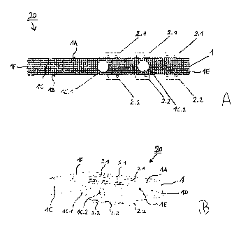
Figure 2 schematically illustrates a high-voltage switch in
accordance with one embodiment in a lateral cross-sectional view
B0029US,
CA 02816468 2013-04-30
, 9
(A) and a perspective view (B) . The high-voltage switch 20 comprises
a cooling substrate 1, which, in terms of construction and
functionality, is embodied identically to the cooling substrate 1
of the exemplary embodiment in figures 1A, 1B and so the details
need not be repeated here. The high-voltage switch 20 furthermore
comprises first high-voltage transistors 2.1 and second
high-voltage transistors 2.2. The first high-voltage transistors
2.1 are applied on a first main surface lA of the cooling substrate
1 and the second high-voltage transistors 2.2 are applied on a
second main surface 1B of the cooling substrate 1. As can be seen
in figure 2A, the first and second high-voltage transistors 2.1 and
2.2 are applied in a manner situated directly opposite one another
in pairs on the first and second main surfaces lA and 1B of the
cooling substrate 1. This will additionally be of significance in
a different context further below.
Figure 3 schematically illustrates a circuit diagram of a
high-voltage switch in accordance with one embodiment. The
high-voltage switch 30 in figure 3 is embodied as a push-pull
circuit, which is connected between a first potential connection
U+ and a second potential connection U-, wherein the first and
second potential connections are connected to the connection
terminals of a high-voltage source. The high-voltage switch 30
substantially consists of two transistor chains 31 and 32
comprising respectively MOS field effect transistors (mosFETs)
T1H - TNH and T1L - TNL, which are respectively connected in series
with regard to their source/drain paths. The MOSFETs T1H - TNH and
T1L - TNL are driven by charging/discharging circuits CL1H - CLNH
and CL1L - CLNL known per se, which are respectively connected to
the gate and source connections of the MOSFETs T1H - TNH and
T1L - TNL.
The high-voltage switch 30 thus comprises a first transistor chain
31, within which first MOSFET transistors T1H - TNH are connected
B0029US CA 02816468 2013-04-30
in series. The drain connection of the MOSFET transistor TNH is
connected to the first voltage pole U+ of the high-voltage source,
while at the other end of the transistor chain the MOSFET transistor
T1H is connected by its source connection to a resistor RLOAD_Ii which,
for its part, is connected to a node 33. The high-voltage switch
30 furthermore comprises a second transistor chain 32 in which the
MOSFET transistors T1L - TNL are connected in series. The MOSFET
transistor T1L is connected by its source connection to the second
voltage pole U- of the high-voltage source, while the MOSFET
transistor TNL is connected by its drain connection to a resistor
RLOAD_L which, for its part, is connected to the node 33. The
resistors RLOADL and RLoAD_R should be understood merely as by way of
example and not mandatory. Therefore, they can also be omitted.
However, in addition to the resistors RLoAD J., and RLoAD_R it is also
possible to insert a further resistor between the node 33 and the
connection point PAD3.
According to the invention, the MOSFETs T1H - TNH and T1L - TNL of
the transistor chains 31 and 32 are mounted on a cooling substrate
1 in accordance with one of the embodiments in figures 1 and 2. One
preferred variant can be formed by the fact that, in accordance with
the embodiment in figure 2, the transistors T1H - TNH of the first
transistor chain 31 are mounted on a first surface 1A of the cooling
substrate 1 and the transistors T1L - TNL of the second transistor
chain 32 are mounted on a second surface 1B of the cooling substrate
1, said second surface being situated opposite the first surface
1A. A particularly advantageous construction arises here if those
transistors of the two transistor chains which spatially and in
terms of potential are equally spaced apart from their associated
voltage pole U+ or U- are arranged opposite one another in each case
in pairs. Thus, the transistor T1L should be arranged opposite the
transistor TNH, T2L opposite T(N-1)H, etc. This is advantageous
since, during the operation of a push-pull circuit, during a
switching process the transistors of one transistor chain are
B0029US, CA 02816468 2013-04-30
A 11
closed, while at the same time the transistors of the other
transistor chain are opened. During such a switching process,
potential changes of identical or similar amplitude then arise in
the transistors at the output side thereof, thus resulting in
particularly low capacitive charge reversals and correspondingly
low electrical losses.
The charging/discharging circuits CL1H - CLNH and CL1L - CLNL are
likewise mounted on the cooling substrate 1 in one preferred
embodiment. They are advantageously mounted on the surface lA of
the cooling substrate 1 in the form of a series in such a way that
each charging/discharging circuit becomes situated directly
alongside the high-voltage transistor assigned to it. The
electrical connections on the cooling substrate 1 can be produced
by any desired techniques known per se. Mention may be made here
of the DCB technique (direct copper bonding) and the AMB technique
(active metal brazing). Likewise, there are techniques known per
se which are used to apply or integrate resistors, inductances and
capacitors on ceramic substrates. By way of example, the resistors
RimILL and RWAILR and connection pads PAD1 - PAD3 shown by way of
example in figure 3 can be applied in this way.
The high-voltage switch shown in figure 3 can be used for a Pockels
cell drive circuit. For this purpose the Pockels cell is connected
between the node 33 (PAD3) with its first electrical connection and
is connected by its second electrical connection to the second
voltage pole U- of the high-voltage source.