Note: Descriptions are shown in the official language in which they were submitted.
CA 02819672 2013-06-27
Electrically Passive Automatic Summing Casino Style Playing Chips
The following description is best understood by those with a background in
electrical
engineering as it pertains to the use of electronic components, electrical
circuit
topologies, advanced mathematical analysis, and applications of logic.
Background Information
Playing chips, or simply chips, are frequently used in games as representative
monetary or countable values. Typically, chips are cylindrical in shape with
heights
significantly less than their corresponding radii. Chips are designed to be
held,
stacked vertically upon each other on a surface, and to collectively indicate
values
corresponding to the chips' previously designated values. Chips are usually
differentiated by colour or visual symbols, indicating their representative
values. For
example, in a game of poker, a white-coloured chip may represent the value of
one
or $1 whereas a red-coloured chip may represent the value of five or $5. The
red-
coloured chip is equivalently valued at the countable or monetary value of
five
white-coloured chips. Similarly, colouring chips different colours may
represent
other monetary or countable values.
Counting or summing the total amount of chips in a stack or several stacks is
a
tedious and time consuming operation. A method for optical scanning to provide
a
basis for automatically allocating player benefits in a gaming environment
exists and
may be found in the following patent:
SOLTYS, RICHARD & HUIZINGA, RICHARD (11) CA 2562516
Patents also exist which involve the placement or method of placement of a
shelled
electronic identification device or microchip; which may consist of memory, a
transceiver, and an antenna; within a playing chip:
1
CA 02819672 2013-06-27
* .
, .
BOIRON, DOMINIQUE (11) CA 2172260
CHAPET, PIERRE (11) CA 2555592
Chips were previously counted manually or, in part, through the use of optical
sensors. Optical sensors may occur difficulties in counting chips hidden
behind
obstacles such as other chips, lighting obstructions, hands, cards, and
whatever else
may be reasonably placed within a gaming environment. Microchips have often
been
used as a means of casino chip security rather than being used to count chips.
Microchip identification through individual chip transceivers has not been
readily
used, and may not be practical, to count large amounts of chips in a public
setting.
Relative costs of the previously mentioned technologies may be rather
cumbersome
as they involve the manufacturing of microchips and optical sensor networks.
Summary Of The Invention
The invention described henceforth provides a reliable way of summing the
representative values of chips without the use of manual counting, microchips,
shelled identification devices, or optical sensors. The invention provides a
reliable
method of summing the representative values of chips by creating an electrical
network by stacking chips upon one another in stacks of zero chips (no chips),
a stack
of one chip or single chip, or a stack of several chips. The chips contain an
electrically
passive component, or combination thereof, in which the element(s) are
electrically
connected to the outer extremities of a chip to create electrically isolated
nodes,
akin to those found in a circuit. A chip can, therefore, conduct electricity
and allow
the passage of current through itself or through other chips stacked upon it.
The
resulting electrical network has specific electrical properties related to the
components embedded within the individual chips. By applying voltages, and
correspondingly currents, to the specified nodes of a stack, an electrical
circuit is
2
CA 02819672 2013-06-27
' =
. .
created which can be used to determine the electrical properties of a stack.
Mapping
the electrical properties of the components placed within the chips to
designated
countable values enables a stack to be countable through electrical
measurement.
The electrical measurement takes place through a mat consisting of electrical
nodes
which can apply potential differences to the stacks within a well defined
surface
area. The mat is designed to apply potential differences to a single stack, or
multiple
stacks regardless of the stack's or stacks' perpendicular displacement(s) to
the mat's
surface such that either faces of the chips are stacked evenly and parallel to
the
mat's surface within the well defined surface boundaries of the mat. By
applying
logic, through hardware and software, the resulting mat measurements result in
a
countable set of the previously designated chip values. The costs associated
with
embedding passive electrical components within a chip are significantly less
than
designing active microchips for placement in individual chips. Collectively,
these
ideas result in electrically passive automatic summing casino style playing
chips
which can be used in a gaming environment.
The figures, listed below, show the general topology of the invention. The
figures are
referenced and explained in detail in the detailed description.
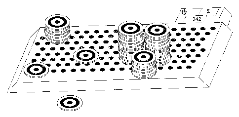
Figure No. 1 is a slightly-elevated frontal view of the invention showing
chips placed
in various places on and around a mat used for counting their designated
values.
Figure No. 2 is a longitudinal cross-section of an electrically passive
playing chip.
Figure No. 3 is a longitudinal cross-section of a stack of playing chips
resting upon a
mat used for measuring the collective electrical characteristics of the stack.
Figure No. 4 shows two circuits for analysing the electrical properties of an
electrically passive playing chip.
3
CA 02819672 2013-06-27
Figure No. 5 is a modification of Figure No. 1 showing the mat without
placement of
chips.
Figure No. 6 is a flow chart for removing duplicated and erroneous
measurements
from the mat's measurements as processed by a microprocessor.
Figure No. 7 is an evaluation of Figure No. 6's flow chart at the node pair of
Nad &
N4.
Figure No. 8 is a duplicate of Figure No. 1 without the use of indicative
markings. It is
used for illustrative purposes.
Detailed Description
A modified chip 1 may be seen from above in Figure No. 1 and sideways through
a
cross-section in Figure No. 2. The chip consists of an electrically conductive
disk 2
situated at the diametric centre of the chip's surface. The disk is embedded
within
the chip and its surface remains flush with the surface of the chip. An
electrically
conductive ring 3, with the same diametric centre as the disk, is situated
around the
disk, separated by the non-conductive insulating natural medium of the chip 4,
typically clay. The natural medium of the chip extends past the outer
perimeter of
the ring 3 to provide an insulating medium between one chip and another 5.
Externally, the chip is rotationally symmetric about its longitudinal axis.
Thus, a
similar disk 6 and ring 7 may be found upon the other face of the chip, as
seen in
Figure No. 2. An electrically conductive medium 8 connects the two disks 2 6
to each
other. The electrically conductive medium 8 also connects to the first
terminal 9 of
the embedded electrically passive component 10. An electrically conductive
medium
11 connects the two rings 3 7 to each other. This electrically conductive
medium 11
also connects to the second terminal 12 of the embedded electrically passive
4
CA 02819672 2013-06-27
'
,
component 10. The result is an externally conductive, electrically passive,
four
terminal 2 3 6 7 chip in which the chip's component 10 may be measured. The
chips
may create new electrical connections by stacking chips upon each other 13,
see
Figure No. 1. It is possible to create more terminals via more rings but their
uses and
applications are not discussed herein.
The electrically passive component placed within a chip, or combination
thereof,
produces an electrically measureable quality when exposed to a voltage or
current
source. This typically constitutes a resistance, capacitance, or inductance.
Diagrammatically, they are labelled as Z 10, as seen in Figure. No. 2, as this
is
common practice upon a passive component's exposure to an AC voltage or
current
source. Both AC and DC applications will be discussed.
The chips, when stacked, create a parallel network of electrically passive
elements
which add in relation to the laws of adding electrically passive elements in
parallel.
This parallel connection is shown in Figure No. 3 which displays a cross
sectional
view of several chips stacked upon each other. The chips, vertically stacked
from the
surface of a mat 14, create an electrical path starting at a node 15. Current
may
traverse the interconnected disks 6 2 through the electrical conducting medium
8 of
the chips. The current travels from chip to chip in a vertical fashion even
though the
chips may be stacked somewhat unevenly 16. The current passes through the
corresponding electrically passive elements of the bottom chip 9 10 12, and
every
chip in the stack, and exits through another node 17 thereby completing the
circuit.
The current has a direct path from the top chip's 18 rings 19 20 to the
exiting node
17 due to the radial symmetry of the chips' electrical connections.
Resistors, when placed in parallel, create both a mathematically and
physically
representable equivalent resistance according to equation 1.
CA 02819672 2013-06-27
" 1
Req = (E )1
Ri
-
By selecting a base resistance value, a countable designation of values may,
fractionally, be associated with the base resistance value. This relationship
is shown
in equation 2.
Base
ChiPvalue =D 2
II Value
As an example; to create a series of chips with designated values of 1, 5, 10,
50;
choose a base value resistance. If a base of Base = 50k0 is chosen, then the
corresponding equivalent resistance values are, respectively, 50k0, 10k0, 5k0,
and
1k0. By applying the mapping shown in equation 2, or similar ones shown in
equations 5 and 6, creating a stack of ten chips valued at one each is
electrically
indistinguishable from a stack of two chips valued at five each or a single
chip valued
at ten. These relationships provide a method for mapping electrical
characteristics of
parallel networks to countable values.
Similar to resistors, other electrically passive elements, including
capacitors and
inductors, may be used in a parallel network with similar governing equations.
Capacitors, when placed in parallel, create a mathematically and physically
representable equivalent capacitance governed by equation 3. Inductors, when
placed in parallel, create a mathematically and physically representable
equivalent
inductance governed by equation 4.
6
CA 02819672 2013-06-27
=
Ceq = Ci 3
i=
n
Leg = (E r I 4
Accordingly, a base value may be assigned to count chips via capacitors, as
seen in
equation 5, or inductors, as seen equation 6. The base capacitance is
accordingly
measured in an SI prefixed value of farads' and the base inductance is
accordingly
measured in an SI prefixed value of henrys.
Chip Vcdue = Base *Cv,1õ, 5
Buse
ChiPvatue =7 6
L.,Vattie
The equivalent resistance, capacitance, or inductance is most easily read by
external
interfaces through a related voltage rather than an intrinsic electrical
property. A
simple way of measuring a voltage associated with the components' intrinsic
properties is through voltage division as shown in Figure No. 4. If an
element, Zeq, is
purely resistive, at DC 21, an output voltage 22 relating to the element's 23
resistance may be calculated through the transfer equation shown in equation
7.
RP*
Vour = 7
RP + Z
eq
At DC 21, if an element 23 is inductive or capacitive, the output voltage 22
relates to
the time constant of the circuit. At AC 24, the element's 25 impedance is
related to
the output voltage 26 via the transfer equation shown in equation 7. The
output
7
CA 02819672 2013-06-27
voltage's magnitude and phase angle can be used to measure electrically
passive
combinations of resistances, capacitances, and inductances by separating the
real
and imaginary portions of the complex impedance. Note that the inductors' and
capacitors' series impedances are respectfully jwLeci and (jwCeqr when
analysed at
AC. Another degree of freedom is added by using combinations of resistances
and
capacitances, or resistances and inductances in conjunction with equations 2,
5, and
6. For example, a resistance could indicate the value of a chip whereas the
capacitance could differentiate one set of chips from another set of chips for
the
purpose of identification. Through these definitions, several electrical
methods of
assigning values or multiple values to chips are possible. Converting the
equivalent
impedance of a chip, or stack of chips, is done through equation 8 for
resistors and
inductors, or through equation 9 for capacitors. Note that in equations 8 and
9, it is
assumed that the impedances are purely real or purely imaginary. Equations 8
and 9
may be used in separate instances evaluated at a real base and an imaginary
base to
resolve combinations of real and imaginary impedances.
Base
ChiPcount = ¨7 8
c_oeq
ChiPCount = Base * Zeg 9
Figure No. 1 and Figure No. 5 show a mat developed to measure the electrical
characteristics of chips so long as the chips are placed on the surface of the
mat 14
within the boundaries defined by the mat's edges 27 28 29 30. Although a
chip's
electrical properties may be measured with two nodes, the mat is designed to
allow
placement of the chips anywhere on the surface 14 of the mat. Chips may be
placed
on the mat in a single stack 31, or in a stack of several chips 13, as seen
solely in
Figure No. 1. The user interface of the mat includes an on/off switch 32, a
button
8
CA 02819672 2013-06-27
used to sum or reset the sum of the total values of chips placed on the mat
33, and a
numeric display 34 showing the total count of all stacked chips placed on the
mat.
Chips not placed 1 on the mat, as seen solely in Figure No. 1, are not
counted. The
mat applies potential differences through metallic nodes 15 17 which are
embedded
in and flush with the mat's surface. The mat is raised above ground level 35
to allow
housing room 36 for the electrical connections and microprocessor to display
the
final count, as seen in Figure No. 1, Figure No. 3, and Figure No. 5.
Figure No. 3 shows a cross-sectional view of a stack of chips as if they were
placed on
nodes 15 17 of the mat's surface 14. The nodes create an electrical
connection,
equivalent to the circuits shown in Figure No. 4. Switches 37 38 are used to
independently complete a node's connection to a voltage source 39 or resistor
40
depending on the type of node. The output voltage 41 is correspondingly
measured
with respect to ground 42, similar to the output voltages 22 26 shown in
Figure No.
4. As shown, jointly, in Figure No. 1, Figure No. 3 and Figure No. 5, reading
from left
to right, every node placed in an odd numbered row 43 44 45 46 is connected to
a
resistor 40 through a switch 37. Every node placed in an even numbered row 47
48
49 50 is connected to a voltage source 39 through a switch 38. The spacing
between
any two nodes 51 is less than the diameter of the disks 2 6 in a chip 1 to
ensure that
one of the disks is always connected to the mat. Different choices of polygons
for
nodes and their corresponding arrangements are possible but the equilateral
triangular lattice of nodes, as shown in Figure No. 5, is sufficient. The
surface
boundaries of the mat 27 28 29 30 are designed to ensure that a chip's top
disk 2 or
bottom disk 6 is always connected to a node on the mat, as seen jointly in
Figure No.
2 and Figure No. 5. A chip's top ring 3 or bottom ring 7, as seen jointly in
Figure No. 2
and Figure No. 3, will automatically be placed upon one or more nodes if this
condition is met.
9
CA 02819672 2013-06-27
,
A microprocessor is used to interface with the mat's electrical hardware. The
microprocessor is used to turn on or turn off switches 37 38 which are
connected to
nodes 17 15, as seen in Figure No. 3. This in turn allows voltage measurement
41 of
completed circuits for software computation by the microprocessor. As shown,
externally, in Figure No. 1, the microprocessor is also used for user
interfacing
purposes to display counts 34 of the chips, enable a manual reset of the count
33, to
turn the device on or off 32, and to interface with any other external devices
such as
another mat, display, or computer.
Software is used to determine the counts of the stacks. Since disks and rings
may
overlap several nodes, it is necessary to remove short circuits and duplicated
counts
from the measured voltages. Open circuits are treated as infinite resistance
and
naturally result in a voltage and count of zero. As seen in Figure No. 1, the
chips are
designed with distance of insulating mediums 5 such that twice that distance
is
greater than the diameter of a node 17. This ensures that two chips never
overlap
the same node. Begin by designating the nodes in the upper left row from left
to
right, as seen in Figure No. 5, with numerals: N1 52, N2, N3, N4 17, ... N18
43.
Designate all other odd numbered rows' nodes with numerals in the same
sequential
left-to-right manner where the third row begins at N19 and ends at N36 and so
forth. In the same manner designate letters to the even numbered rows starting
at
row two: Naa 53, Nab, Nac, Nad, Nae 15, ... Nar 47. For convenience, continue
the
lettering of row four with the following: Nba, Nbb, Nbc, ..., Nbq 48. Continue
this
pattern until all nodes are labelled. Use the microprocessor to turn on every
adjacent pair of voltage to resistor nodes, measuring and recording the output
voltage every time. For rows one and two this would be: (Naa & N1), (Nab &
N1),
(Nab & N2), (Nac & N2), (Nac & N3), (Nad & N3), ... (Nar & N18). For rows two
and
three, this would be: (Naa & N19), (Naa & N20), (Nab & N20), .... (Nar & N36).
CA 02819672 2013-06-27
. '
Once every pair has been recorded, remove all measured short circuits (V.ut >
Vthreshold where Vthreshold -*".''' Nilo)/ test the equivalence of every
physically adjacent pair
of circuits to remove duplicated counts, and count the remaining non-
duplicated
node pairs. Sequentially this reads as follows. Set the measured results from
the
node pair to zero if it was a short circuit. Record the voltage of the
measurement.
Test the node pair against the next node pair to determine if they have the
same
measurement (this indicates a duplicated count). If a duplicated measurement
occurred, then set all measurements associated with the individual nodes of
the
current node pair and the next node pair to zero. If there was not a
duplicated
measurement and a non-zero measurement exists at the current node pair then
set
all measurements associated with the individual nodes of the current pair to
zero.
This logic is shown in the flow chart in Figure No. 6 and again with the flow
chart
evaluated at a pair of nodes, Nad & N4, in Figure No. 7.
Convert the measured voltages to chip counts depending on the choice of
equations
8, 9 in conjunction with equation 7. Add up the results to obtain the final
summation
of all chip values stacked on the mat. As the count is a digital value, it can
be used for
display or to interface with other devices to perform calculations such as
chip ratios
and betting odds.
11