Note: Descriptions are shown in the official language in which they were submitted.
CA 02820002 2013-06-04
DESCRIPTION
TITLE OF INVENTION
SOLAR CELL AND SOLAR-CELL MODULE
TECHNICAL FIELD
[0001]
This invention relates to a solar cell and solar cell
module having the advantages of low cost and high efficiency.
BACKGROUND ART
[0002]
FIG. 1 illustrates one general solar cell of mass
ls production model using a mono- or polycrystalline silicon
substrate. The solar cell includes a p-type silicon
substrate 101 obtained by doping monocrystalline silicon with
a dopant such as B or Ga. An emitter layer 102 is formed in
a light-receiving surface of silicon substrate 101 by heat
treatment to diffuse a dopant for imparting n-type
conductivity such as P or Sb into silicon substrate 101 in a
high concentration. A plurality of extraction electrodes 104
of several hundreds to several tens of microns ( m) wide are
disposed contiguous to the emitter layer 102 for extracting
photogenerated electric charge from substrate 101. Also,
several collector electrodes 105 of several millimeters (mm)
wide are disposed for collecting the charges drawn in
extraction electrodes 104 and interconnecting solar cells
together. While these electrodes may be formed by various
methods, one method commonly employed from the standpoint of
cost is by printing a metal paste comprising fine particles
of metal such as Ag and an organic binder through a screen or
the like, and heat treating at a temperature of several
hundreds to about 850 C for bonding to the substrate. On the
surface of the substrate opposite to the light-receiving
surface, a back electrode 107 of opposite polarity to the
light-receiving side electrode is formed by using a metal
-1-
CA 02820002 2013-06-04
paste comprising fine particles of metal such as Al or Ag and
an organic binder, screen printing, and firing at a
temperature of about 700 to 850 C. Between silicon substrate
101 and back electrode 107, an electric field layer 106
containing a dopant for imparting the same p-type conductivity
as the substrate such as Al, B or Ga in a high concentration
is formed for efficiently extracting charge generated on the
back side to the outside. Further, in the region where light
is incident on the solar cell, a passivation film 103 is
a formed for optical confinement. A silicon nitride film which
is formed by chemical vapor deposition (CVD) or the like is
commonly used as the passivation film.
[0003]
The passivation film also has a further important
function of passivating the silicon surface. In the interior
of crystals, silicon atoms are in a stable state due to the
covalent bond between adjacent atoms. However, at the
surface corresponding to the terminus of atom arrangement,
where no adjacent atom to be bonded is available, an unstable
energy level known as "dangling bond" appears. Since the
dangling bond is electrically active, it captures and
extinguishes charge photogenerated within silicon, detracting
from the operation of a solar cell. Thus, the solar cells
have been subjected to surface passivating treatment or
otherwise treated to form an electric field such that
photogenerated carriers may not be captured by dangling bonds.
A silicon nitride film formed by CVD is widely used because
its optical properties are suited for silicon solar cells and
because the film itself has a positive fixed charge and also
has a high passivation effect due to the inclusion of much
hydrogen capable of passivating dangling bonds.
[0004]
On the other hand, in the emitter layer where electric
charge is present at a high density, direct recombination of
electrons and holes, known as Auger recombination, becomes
outstanding, detracting from the operation of a solar cell.
Also, a photon-absorption phenomenon by free charge, known as
-2-
CA 02820002 2013-06-04
free carrier absorption, becomes prominent to reduce the
amount of photogenerated charge. Accordingly, the dopant
concentration of the emitter layer should desirably be kept
as low as possible or the depth of the emitter layer should
desirably be shallow. However, reducing the dopant
concentration, in turn, increases the contact resistance
between silicon and metal electrode, giving rise to the
problem of an increased resistance loss of generated power.
Also formation of a shallow emitter layer is difficult to
control, making it difficult to maintain a high production
yield on the mass production level. Even if a shallow
emitter layer can be formed, the electrode can penetrate
through the emitter layer during electrode formation
including firing step. This frequently results in a
phenomenon that no solar cell performance is available.
[0005]
Approaches for avoiding these problems include a
method of selectively adding a dopant to an electrode-forming
region in a high concentration while adding no dopant to a
non-electrode-forming region (known as "localized doping"),
and a method of adding a dopant in a relatively low
concentration (known as "double doping").
[0006]
The localized doping structure or double doping
structure is generally formed by forming a dielectric film of
several hundreds of nanometers (nm) such as a silicon oxide or
silicon nitride film on substrate surface as diffusion barrier,
opening an electrode-forming portion of the dielectric film by
photolithography (see, for example, J. Knobloch, A. Noel, E.
Schaffer, U. Schubert, F. J. Kamerewerd, S. Klussmann, W.
Wettling, Proc. the 23rd IEEE Photovoltaic Specialists
Conference, p.271, 1993), etching paste (see, for example,
JP-A 2003-531807), or laser ablation, and heat treating in a
heat-treatment furnace for vapor phase diffusion of a dopant
only through the opening. These methods, however, are not
suited at all for mass production because they include complex
steps or need expensive materials or apparatus.
-3-
= CA 02820002 2013-06-04
[0007]
One simpler method suited for mass production is by
premixing a dopant in a conductive paste as the
electrode-forming material, as proposed in, for example, D. L.
Meier, H. P. Davis, R. A. Garcia, J. A. Jessup, Proc. the
28th IEEE Photovoltaic Specialists Conference, p.69, 2000.
With this method, P is added to Ag paste as dopant, for
example, the paste is printed onto a silicon substrate, and
the paste is fired at or above the eutectic point of Ag and
lo Si. While the portion of silicon onto which the Ag paste has
been applied is once melted and recrystallized upon cooling,
P in the Ag paste is taken into the silicon, whereby a high
concentration P-doped region is formed immediately below the
electrode-forming portion. This method is commonly referred
to as "self-doping" and the conductive paste for implementing
the method is referred to as "self-doping paste." The above
article reports that the method actually results in a good
electrical contact between Ag and Si.
[0008]
On the other hand, the self-doping paste contains a
dopant for forming a self-doped region, an additive for
effectively forming a high-concentration doping layer, and
the like in relatively high proportions. For this reason,
while the self-doping paste provides a good electrical
contact between electrode and silicon, the content of metal
particles contributing to the conduction of charge extracted
from the silicon substrate must be kept low. As a result,
the sintered body of self-doping paste has a high
interconnect resistance, giving rise to the problem that the
output of the solar cell is reduced.
SUMMARY OF INVENTION
Technical Problem
[0009]
An object of the invention which is made under the
aforementioned circumstances is to provide a solar cell and
solar cell module having the advantages of a good electrical
-4-
CA 02820002 2013-06-04
contact between a silicon substrate and an extraction
electrode, a reduced loss by electrode interconnect
resistance, and excellent cell characteristics.
Solution to Problem
[0010]
Making extensive investigations to attain the above
object, the inventors have found that if a first electrode in
the form of a sintered body of conductive paste containing a
dopant for imparting conductivity to silicon is used as the
extraction electrode, and a second electrode having a higher
conductivity than the first electrode is used as the
collector electrode, then the loss by contact resistance
between silicon substrate and the extraction electrode and
the loss by electrode resistance are reduced and solar cell
characteristics are drastically improved. The invention is
predicated on this finding.
[0011]
Accordingly, the invention provides a solar cell and
solar cell module as defined below.
[1] A solar cell comprising a crystalline silicon
substrate of one conductivity type having a light-receiving
surface, an emitter layer formed on the light-receiving
surface side of the substrate and having a dopant of opposite
conductivity type added thereto, a passivation film formed on
the surface of the substrate, an extraction electrode for
extracting photogenerated charge from the silicon substrate,
and a collector electrode in contact with at least a portion
of the extraction electrode for collecting the charge drawn
in the extraction electrode, characterized in that the
extraction electrode includes a first electrode in the form
of a sintered conductive paste containing a dopant for
imparting conductivity to silicon, at least the first
electrode is formed so as to penetrate through the
passivation layer, and the collector electrode includes a
second electrode having a higher conductivity than the first
electrode.
-5-
CA 02820002 2013-06-04
[2] The solar cell of [1] wherein below the interface
between the emitter layer of the silicon substrate and the
first electrode, a self-doped region is formed as a result of
the dopant in the first electrode being diffused during the
sintering step.
[3] The solar cell of [1] or [2] wherein the self-doped
region has a lower resistivity than the emitter layer
disposed adjacent thereto.
[4] The solar cell of any one of [1] to [3] wherein the
first electrode is formed of a conductive paste based on Ag
and containing B, Al, Ga, P, As, In or Sb alone or a compound
thereof or a combination thereof as the dopant.
[5] The solar cell of any one of [1] to [4] wherein the
first electrode is partially contacted or entirely overlaid
with the second electrode.
[6] The solar cell of any one of [1] to [5] wherein the
extraction electrode has a laminate structure consisting of
the first and second electrodes, and the collector electrode
has a monolayer structure consisting of the second electrode.
[7] The solar cell of any one of [1] to [5] wherein the
extraction electrode and the collector electrode each have a
laminate structure consisting of the first and second
electrodes.
[8] The solar cell of any one of [1] to [5] wherein the
extraction electrode consists of the first electrode, and the
collector electrode consists of the second electrode.
[9] The solar cell of any one of [1] to [8] wherein the
passivation film comprises silicon oxide, silicon nitride,
silicon carbide, aluminum oxide, amorphous silicon,
microcrystalline silicon or titanium oxide or a combination
thereof.
[10] A solar cell comprising a crystalline silicon
substrate having a non-light-receiving surface, a passivation
film formed on the non-light-receiving surface of the
substrate, an extraction electrode for extracting
photogenerated charge from the silicon substrate, and a
collector electrode disposed at least partially in contact
-6-
CA 02820002 2013-06-04
with the extraction electrode for collecting the charge
collected in the extraction electrode, characterized in that
the extraction electrode includes a first electrode in the
form of a sintered conductive paste containing a dopant for
imparting conductivity to silicon, at least the first
electrode is formed so as to penetrate through the
passivation layer, and the collector electrode includes a
second electrode having a higher conductivity than the first
electrode.
lo [11] The solar cell of [10] wherein at the interface
between the silicon substrate and the first electrode, a
self-doped region is formed as a result of the dopant in the
first electrode being diffused during the sintering step.
[12] The solar cell of [10] or [11] wherein the self-doped
region has a lower resistivity than a non-self-doped region
disposed adjacent thereto.
[13] The solar cell of any one of [10] to [12] wherein the
first electrode is formed of a conductive paste based on Ag
and containing B, Al, Ga, P, As, In or Sb alone or a compound
thereof or a combination thereof.
[14] The solar cell of any one of [10] to [13] wherein the
first electrode is partially contacted or entirely overlaid
with the second electrode.
[15] The solar cell of any one of [10] to [14] wherein the
extraction electrode has a laminate structure consisting of
the first and second electrodes, and the collector electrode
has a monolayer structure consisting of the second electrode.
[16] The solar cell of any one of [10] to [14] wherein the
extraction electrode and the collector electrode each have a
laminate structure consisting of the first and second
electrodes.
[17] The solar cell of any one of [10] to [14] wherein the
extraction electrode consists of the first electrode, and the
collector electrode consists of the second electrode.
[18] The solar cell of any one of [10] to [17] wherein the
passivation film comprises silicon oxide, silicon nitride,
silicon carbide, aluminum oxide, amorphous silicon,
-7-
CA 02820002 2013-06-04
microcrystalline silicon or titanium oxide or a combination
thereof.
[19] A solar cell module comprising electrically connected
solar cells according to any one of [1] to [18].
Advantageous Effects of Invention
[0012]
In a solar cell comprising extraction and collector
electrodes, a self-doping electrode and a high conductivity
lo electrode are used as the extraction electrode and collector
electrode, respectively. Then the loss by silicon-electrode
contact resistance and the loss by electrode resistance are
reduced and at the same time, optical and electric losses in
the emitter layer are reduced. Solar cell characteristics
are drastically improved. Also, the process can be
implemented by conventional screen printing and similar
techniques, which is quite effective for cost savings.
BRIEF DESCRIPTION OF DRAWINGS
[0013]
FIG. 1 is a schematic perspective view of an exemplary
structure of a conventional solar cell.
FIG. 2 is a schematic perspective view of an exemplary
structure of a solar cell in one embodiment of the invention.
FIG. 3 is a schematic perspective view of an exemplary
structure of a solar cell in another embodiment of the
invention.
FIG. 4 is a schematic perspective view of an exemplary
structure of a solar cell in a further embodiment of the
invention.
FIG. 5 is a plan view of a printing plate for use in
electrode formation according to the invention, (a) showing a
pattern of extraction electrode alone, (b) showing a pattern
of collector electrode alone, and (c) showing a combined
pattern of extraction and collector electrodes.
-8-
CA 02820002 2013-06-04
FIG. 6 is a schematic perspective view of an exemplary
structure of a solar cell in a yet further embodiment of the
invention.
FIG. 7 is a schematic perspective view of an exemplary
structure of a solar cell in a still further embodiment of
the invention.
FIG. 8 is a diagram illustrating values of
interconnect resistance and contact resistance in Example and
Comparative Example.
DESCRIPTION OF EMBODIMENTS
[0014]
Referring to FIGS. 2 to 8, several embodiments of the
invention are described below. Like reference characters
designate like or corresponding parts throughout the several
views while their description is sometimes omitted.
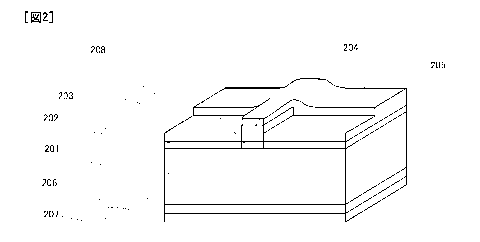
FIG. 2 illustrates a solar cell in one embodiment of
the invention. The solar cell includes a crystalline silicon
substrate 201 of one conductivity type, an emitter layer 202
formed on the silicon substrate 201 and having a dopant of
opposite conductivity type added thereto, a passivation film
203 formed on the surface of the emitter layer 202, an
extraction electrode for extracting photogenerated electric
charge from the silicon substrate 201, and a collector
electrode for collecting the charge drawn in the extraction
electrode, wherein the electrodes are formed by printing and
firing conductive paste. The extraction electrode includes a
first electrode 204 in the form of a sintered body of
conductive paste containing a dopant for imparting the same
conductivity type as the emitter layer to silicon. The first
electrode 204 is formed so as to penetrate through the
passivation layer 203, and at the same time, a self-doped
region 208 into which the dopant from the first electrode 204
is diffused at a high concentration is formed immediately
below the first electrode 204. This enables to establish a
good electrical contact between the first electrode 204 and
the silicon substrate 201 and to reduce the dopant
-9-
= CA 02820002 2013-06-04
concentration or depth of the emitter layer 202, and
eventually to ameliorate any degradation of solar cell
characteristics due to carrier recombination and free carrier
absorption in the emitter layer. Further the collector
electrode includes a second electrode 205 having a higher
conductivity than the first electrode 204, which enables to
significantly reduce the output power loss of the solar cell
by interconnect resistance.
Notably, an electric field layer 206 and a back
electrode 207 are illustrated.
[0015]
Now, one exemplary method of fabricating a solar cell
according to the invention is described. The invention is
not limited to the solar cell fabricated by this method.
[0016]
An as-cut monocrystalline {100} p-type silicon
substrate in which high purity silicon is doped with a Group
III element such as B or Ga so as to give a resistivity of
0.1 to 5 Q-cm is etched with a conc. alkali solution of
sodium hydroxide or potassium hydroxide having a
concentration of 5 to 60% by weight or mixed acid of
hydrofluoric acid and nitric acid for removing the work
damaged surface layer. The monocrystalline silicon substrate
may have been prepared by either the CZ or FZ method.
[0017]
Subsequently, the substrate surface is provided with
microscopic asperities known as texture. The texture is an
effective means for lowering the reflectivity of solar cells.
The texture may be readily provided by immersing the
substrate in a hot alkaline solution of sodium hydroxide,
potassium hydroxide, potassium carbonate, sodium carbonate,
sodium hydrogencarbonate or tetramethylammonium hydroxide
(concentration 1 to 10 wt%) at a temperature of 60 to 100 C
for about 10 to about 30 minutes. Often, a proper amount of
2-propanol is dissolved in the alkaline solution to control
the reaction.
-10-
CA 02820002 2013-06-04
[0018]
The texturing is followed by washing with an aqueous
acidic solution such as hydrochloric acid, sulfuric acid,
nitric acid or hydrofluoric acid or a mixture thereof.
Washing with hydrochloric acid is preferred from the cost and
property standpoints. To enhance cleanness, washing may be
carried out by mixing 0.5 to 5 wt% of aqueous hydrogen
peroxide with aqueous hydrochloric acid and heating at 60 to
90 C.
[0019]
On the substrate, an emitter layer is formed by vapor
phase diffusion using phosphorus oxychloride. The P
concentration and depth of the emitter layer are determined
by a balance of resistance to current flow through the
emitter layer and surface passivation effect, or the like.
Typically, they are determined such that the emitter layer
may have a sheet resistance of 50 to 400 ohm/square (Q/D) as
measured by the four probe method.
[0020]
In common silicon solar cells, a p-n junction must be
formed only on the light-receiving surface. To this end,
suitable means must be taken for avoiding any p-n junction on
the back surface, for example, by carrying out diffusion
while two substrates are mated together, or by etching away
the diffusion layer on one side in aqueous alkaline solution
or the like. At the end of diffusion, the glass formed on
the surface is removed using hydrofluoric acid or the like.
[0021]
Next, an antireflection/passivation film is formed on
the light-receiving surface. Using a chemical vapor
deposition system for film formation, a silicon nitride or
similar film is deposited to a thickness of 80 to 125 nm,
typically about 100 nm. Often a mixture of monosilane (SiH,)
and ammonia (NH3) is used as the reactant gas although
nitrogen may be used instead of NH3. Also the desired
refractive index may be obtained by using H, gas to dilute
the film-forming species, to adjust the process pressure, or
-11-
CA 02820002 2013-06-04
to dilute the reactant gas. The film is not limited to
silicon nitride, and instead, silicon oxide, silicon carbide,
aluminum oxide, amorphous silicon, microcrystalline silicon
or titanium oxide may be used while it may be formed by heat
treatment, atomic layer deposition or the like as well as
chemical vapor deposition.
[0022]
Next, a first electrode is formed on the emitter layer.
For the first electrode, for example, a silver paste is used
lo which is prepared by mixing silver powder, glass frit and
dopant with an organic binder.
[0023]
Since the conductivity type of the emitter layer in
this embodiment is n-type, the dopant used herein is a Group
V element such as P, In or Sb alone or a compound thereof or
a combination thereof. The composition of the paste must be
adjusted depending on the structure and type of a solar cell.
When diphosphorus pentoxide is used, for example, it is
formulated in a proportion of about 0.1 to 30% by weight,
preferably 2 to 15% by weight. The type and amount of the
organic binder are well known.
[0024]
The paste is screen printed and fired or heat treated
to establish conduction between the electrode and the silicon.
This heat treatment is known as a fire-through phenomenon
that during firing of silver paste, the silicon nitride film
reacts with the glass frit and is thus decomposed, allowing
the Ag particles to penetrate through the silicon nitride
film to make electrical contact with the substrate. The
fire-through technique is widely used in the manufacture of
crystalline silicon solar cells.
[0025]
Although the dopant in the silver paste diffuses, in
part, into the silicon substrate to achieve self-doping even
on heat treatment at a temperature of about 700 to 800 C in
the electrode firing temperature range commonly employed,
firing at a temperature equal to or higher than 835 C, the
-12-
CA 02820002 2013-06-04
eutectic point of Ag and Si, is recommended in order to form
a self-doped region more effectively. On firing at or above
the temperature, silicon reacts with silver and melts, and
then recrystallizes while taking in additive dopant. As such,
high concentration doping is accomplished, making a better
electrical contact between the sintered silver and silicon.
[0026]
The electrical contact resistance between silicon and
electrode is correlated to the carrier concentration, that is,
lo dopant concentration on silicon surface and the electrode
material. Where an electrical contact is made between
conventional printed silver electrode and silicon, it is
believed that the dopant concentration on silicon surface
must be at least 1x1019 cm-3, preferably at least 5x1019 cm-3.
[0027]
The dopant concentration may be directly measured by
secondary ion mass spectroscopy (SIMS) or the like. This
quantitative measurement, however, is scarcely used in the
production site because preparation of a sample is cumbersome
and measurement requires skill.
[0028]
For simpler measurement, the spreading resistance
method is utilized. Specifically, the method is by abutting
two metal probes against a silicon substrate, conducting
current flow between the two points, and measuring a voltage
drop thereacross. The spreading resistance is the voltage
drop divided by the current value. Since the voltage drop
occurs in principle at a minute domain near the contact point
of the probe, this method enables evaluation of the minute
domain. If the contact area between the probe and the silicon
substrate is recognized, then the resistivity relative to the
dopant concentration on silicon surface may be determined.
[0029]
In order that the self-doped region function effectively,
the resistivity of the region at its surface should preferably
be 10 mQ-cm or less, more preferably 2 mQ-cm or less. The
lower limit is usually at least 0.5 mQ-cm though not critical.
-13-
CA 02820002 2013-06-04
[0030]
Also, the resistivity of the emitter layer (formed in
the light-receiving area) at its surface should preferably be
as high as possible from the standpoint of suppressing the
aforementioned optical loss and carrier recombination loss,
but should preferably be somewhat low from the standpoint of
increasing the photovoltage. That is, the resistivity of the
emitter layer at its surface should fall in an optimum range.
The optimum range is 5 to 50 mQ-cm though it varies with the
lo structure of a solar cell. On the other hand, to take the
maximum advantage of dual doping structure, the emitter layer
should be designed and controlled such that the resistivity
of the emitter layer at its surface may be higher than the
resistivity of the self-doped region.
[0031]
After the first electrode is formed in this way, a
second electrode is formed on the first electrode by screen
printing and firing.
[0032]
The second electrode should be endowed with a higher
conductivity than the first electrode for the purpose of
suppressing the interconnect resistance loss when the charge
extracted from the silicon substrate to the first electrode
flows to the collector electrode. Such an electrode may be
prepared using a silver paste containing a higher proportion
of silver particles, for example. The resistivity of the
second electrode which is preferably lower should desirably
be up to 5 RQ-cm at most, more preferably up to 3 RQ-cm.
[0033]
With respect to the sequence of firing first and
second electrodes, the steps of printing and firing the first
electrode and the steps of printing and firing the second
electrode may be separately performed as mentioned above.
Alternatively, after the first electrode is printed and dried,
the second electrode is printed, and single heat treatment is
effected for firing both the electrodes at the same time.
-14-
CA 02820002 2013-06-04
[0034]
With respect to the extraction electrode and collector
electrode, the extraction electrode may have a laminate
structure consisting of first and second electrodes, and the
collector electrode have a monolayer structure consisting of
a second electrode as shown in FIG. 2. Alternatively, the
extraction electrode may have a monolayer structure
consisting of a first electrode, and the collector electrode
have a monolayer structure consisting of a second electrode,
lo as shown in FIG. 3.
[0035]
Also, the extraction electrode and collector electrode
each may have a laminate structure consisting of first and
second electrodes as shown in FIG. 4.
[0036]
The structure of these electrodes may be prepared, for
example, by screen printing an electrode paste to form, in
case of the first electrode, a pattern consisting solely of
extraction electrodes as shown in FIG. 5(a), or a pattern of
both extraction and collector electrodes as shown in FIG.
5(c), and in case of the second electrode, a pattern as shown
in FIG. 5(c) or a pattern consisting solely of collector
electrodes as shown in FIG. 5(b).
[0037]
The electrode forming method is not limited to screen
printing and may be performed by inkjet printing, dispenser,
intaglio printing, aerosol spraying or the like. An electrode
having a structure as shown in FIG. 4 may be prepared by
effecting metallization, with the first electrode serving as
seed, to form the second electrode. For metallization,
electroplating, electroless plating or photo-plating is
applicable.
[0038]
In an embodiment wherein the collector electrode is a
monolayer structure consisting of the second electrode, the
second electrode may penetrate through the passivation layer
203, for example, by fire-through capability, until it
-15-
CA 02820002 2013-06-04
contacts the emitter layer 202, as shown in FIGS. 2 and 3, or
may not penetrate through the passivation layer 203 as shown
in FIG. 6.
[0039]
The embodiment of FIG. 6 wherein the passivation film
immediately below the collector electrode is left intact
inhibits recombination of carriers at the silicon surface in
this portion, thus improving solar cell characteristics. The
fire-through capability of electrode paste to penetrate
lo through the passivation film is tailored by the amount of
low-softening-point glass frit added. Accordingly, the second
electrode may be formed using a high-temperature firing paste
containing a relatively small amount of glass frit or free of
glass frit, or a low-temperature cure resin paste.
[0040]
The back electrode is formed by mixing aluminum powder
with an organic binder and screen printing the resulting
paste. Printing is followed by firing at a temperature of
700 to 900 C for 5 to 30 minutes to form the back electrode
and an electric field layer.
[0041]
It is noted that the electric field layer may also be
formed by vapor phase diffusion of boron bromide, for example.
In this case, it is preferred from the standpoint of
suppressing interconnect resistance to use silver paste to
form the back electrode.
[0042]
Firing of the back electrode and the light-receiving
surface electrode may be performed at a time. Also, the order
of forming electrodes on opposite surfaces may be reversed.
[0043]
Back-applied embodiment
The electrode constructed by combining first and
second electrodes according to the invention is also
applicable to the non-light-receiving surface of the solar
cell. FIG. 7 illustrates an embodiment wherein the electrode
of the invention is applied to both the light-receiving
-16-
CA 02820002 2013-06-04
surface and the non-light-receiving surface. While the
p-type silicon solar cell uses the silicon substrate 401 of
p-type conductivity, this embodiment is such that the
self-doped region 407b formed immediately below the
non-light-receiving side first electrode 404b is of p-type
conductivity and the self-doped region 407a on the
light-receiving side is of n-type conductivity. Thus, a
self-doping paste containing a Group V element is used for
the light-receiving side first electrode 404a and a
lo self-doping paste containing a Group III element is used for
the non-light-receiving side first electrode 404b. Also
illustrated are an emitter layer 402, a passivation layer
403a, and collector electrodes 405a and 405b.
[0044]
Such a structure on the non-light-receiving side
allows the non-electrode-forming surface to be covered with
the electric field layer 406 and passivation film 403b,
enhancing the collection efficiency of photogenerated
carriers. It is noted that the electric field layer 406 may
not be formed where the passivation film has a fully high
passivation effect.
[0045]
The shape and construction of first and second
electrodes 404b and 405b on the non-light-receiving side may
be the same as the electrodes on the light-receiving side in
FIGS. 2 to 6. Specifically, the extraction electrode on the
non-light-receiving side may have a laminate structure
consisting of first and second electrodes, and the collector
electrode have a monolayer structure consisting of a second
electrode; the extraction or collector electrode may have a
monolayer structure consisting of a first or second
electrode; or the extraction electrode and collector
electrode each may have a laminate structure consisting of
first and second electrodes.
[0046]
Also, where the collector electrode on the
non-light-receiving side has a monolayer structure consisting
-17-
CA 02820002 2013-06-04
of second electrode 405b as in FIG. 7, the second electrode
405b may penetrate through the passivation layer 403b until
it contacts the field effect layer 406 or silicon substrate
401, as shown in FIG. 7, or may not penetrate through the
passivation layer.
[0047]
On the non-light-receiving surface, a reflector (not
shown) is preferably provided for taking in again the light
transmitted by the substrate. Although the reflector may be
a film of aluminum or silver formed by vacuum evaporation or
the like, a sufficient reflector effect is obtainable simply
by using a white backsheet or the like on the solar cell
module without any additional treatment. Absent the
reflector, electricity generation is yet possible by causing
scattering light to enter from the back surface or by placing
the solar cell such that the non-light-receiving surface may
become a light-receiving side.
[0048]
N-type substrate embodiment
Although the solar cell of the invention is described
by referring to the embodiments using p-type silicon
substrates, the invention is equally applicable to a solar
cell using an n-type silicon substrate.
[0049]
In this embodiment, when reference is made to the
structure of FIG. 7, silicon substrate 401, electric field
layer 406 and self-doped region 407b on the
non-light-receiving side are of n type and the emitter layer
402 and self-doped region 407a on the light-receiving side
are of p type.
[0050]
Herein, the silicon substrate 401 is a n-type
crystalline silicon substrate which is prepared by doping
high-purity silicon with a Group V element such as P or Sb to
give a resistivity of 0.1 to 5 Q-cm. The emitter layer 402
may be formed when the silicon substrate is doped with boron
by vapor phase diffusion using boron bromide, for example.
-18-
CA 02820002 2013-06-04
Also the electric field layer may be formed by vapor phase
diffusion using phosphorus oxychloride, for example. The
self-doped layer 407a on the light-receiving side is formed
using a self-doping paste containing a Group III element such
as B, Al, Ga or In alone or a compound thereof or a
combination thereof. The self-doped layer 407b on the
non-light-receiving side is formed using a self-doping paste
containing a Group V element such as P, As or Sb alone or a
compound thereof or a combination thereof.
lo [0051]
A plurality of solar cells according to the invention
may be electrically connected and used as a solar cell module.
In this embodiment, the connection may be made by any
well-known methods.
EXAMPLES
[0052]
Examples and Comparative Examples are given below by
way of illustration and not by way of limitation.
[0053]
Examples and Comparative Examples
To demonstrate the benefits of the invention, a solar
cell having a conventional electrode structure and a solar
cell having an electrode structure according to the invention
are compared for electricity generating ability.
[0054]
There were provided 90 as-cut boron-doped (100} p-type
silicon substrates of 125 mm square having a diffusion depth
of 250 Nm and a resistivity of 1 Q-cm. The substrates were
immersed in a hot conc. potassium hydroxide aqueous solution
to remove the work damaged layer, immersed in a potassium
hydroxide/2-propanol aqueous solution to form a texture, and
then washed in a hydrochloric acid/hydrogen peroxide mixture.
Next, the substrates, with their back surfaces mated, were
heat treated at 870 C in a phosphorus oxychloride atmosphere,
for doping the light-receiving surface with phosphorus to
form a p-n junction having a sheet resistance of 90 Wo.
-19-
CA 02820002 2013-06-04
Thereafter, the diffusion layer on the non-light-receiving
surface was etched away with fluoronitric acid, and
phosphorus glass was removed with hydrofluoric acid, followed
by washing with deionized water and drying.
[0055]
Thereafter, using a plasma-enhanced CVD system, a
silicon nitride film was formed over the sample surface on
the light-receiving side as a passivation film.
[0056]
lo At this point of time, the substrates were divided
into three groups (1), (2) and (3), each consisting of 30
substrates. Each of different silver pastes (see below) was
printed on the substrates as a light-receiving side electrode
using a printing screen having a pattern of extraction and
collector electrodes on a common screen as shown in FIG. 5(c).
With respect to the printing conditions of electrode paste,
conditions were previously selected and for each set of
conditions, printing conditions such as printing pressure and
squeeze angle were controlled such that an equivalent line
width and cross-sectional area were obtained at the end of
firing.
[0057]
Group (1) is a comparative example by the prior art
technique. As the first electrode, ordinary fire-through
type high-temperature firing paste (paste A) was screen
printed and dried. Then, high-conductivity silver paste
(paste B) was screen printed as the second electrode so that
the first electrode was completely overlaid therewith.
Thereafter, firing at 830 C or optimum condition was carried
out in the ambient (air) atmosphere.
[0058]
Group (2) is another comparative example by the prior
art technique. As the first electrode, fire-through type
self-doping silver paste (paste C) having a phosphorus
compound added so that the self-doped region might have a
resistivity of 2 m52-cm was screen printed and dried. Then,
paste C was again screen printed as the second electrode so
-20-
CA 02820002 2013-06-04
that the first electrode was completely overlaid therewith.
Thereafter, firing at 880 C or optimum condition was carried
out in the ambient atmosphere.
[0059]
Group (3) is an example of the invention. Paste C was
screen printed and dried as the first electrode, and paste B
was screen printed as the second electrode so that the first
electrode was completely overlaid therewith. Thereafter,
firing at 880 C or optimum condition was carried out in the
lo ambient atmosphere.
[0060]
Next, all the solar cells on their back surface were
coated with aluminum paste over their entire sample surface.
Thereafter, firing at 780 C or optimum condition was carried
out in the ambient atmosphere.
[0061]
For the solar cells of the three groups, the shape of
light-receiving side electrode was examined by selecting 5
samples from each group, and measuring the line width and
cross-sectional area of the electrode at nine (9) positions
within the sample surface under a laser microscope. Table 1
reports an average of measurements for each group,
demonstrating that electrodes of equivalent shape were
obtained for all the groups.
[0062]
Table 1
1st
2ndLne width Cross-sectional
ii
Group No. electrode electrode area
(Rm)
paste paste (W112)
(1) Prior art A B 109 1107
(2) Prior art C C 111 1079
(3) Invention C B 106 1083
-21-
CA 02820002 2013-06-04
[0063]
Next, all the solar cells were measured for cell
characteristics by a current-voltage tester using simulative
sunlight with AM 1.5. Table 2 reports an average of solar
cell characteristics for each group, demonstrating that the
solar cells of group (3) within the scope of the invention
show the best cell characteristics.
[0064]
Table 2
Short-circuit Open-circuitConversion
Fill factor
Group No. current voltage
efficiency
(%)
(mA/cm2) (V) (%)
(1) Prior art 35.0 0.636 76.6
17.1
(2) Prior art 35.1 0.635 78.2
17.4
(3) Invention 35.0 0.635 79.4
17.6
[0065]
Next, 15 samples were selected from each group and
measured for contact resistance between silicon substrate and
electrode and interconnect resistance. Determination of
contact resistance was by the ladder method. Determination
of interconnect resistance was carried out by cutting out an
extraction electrode portion from the solar cell sample,
placing probes at opposite ends of the electrode and
measuring current-voltage values.
[0066]
FIG. 8 illustrates relative values of the two
resistances for each group, provided that the average value
of samples of group (1) is 1. It is seen that the samples of
group (3) having the electrode structure according to the
invention have a low contact resistance. It is thus
concluded that the samples of group (3) show the highest fill
factor in Table 2 as a result of the contact resistance and
interconnect resistance being suppressed.
-22-