Note: Descriptions are shown in the official language in which they were submitted.
CA 02822138 2013-08-22
TRANSCEIVER FILTER AND TUNING
BACKGROUND
[0001] In modern radios such as those used in cellular telephones, a high
performance receiver path is used to detect signals below -110dBm in the
presence
of blocking signals up to -20dBm. This makes design of the radio and the
frequency synthesizer challenging in terms of reducing power consumption. The
receiver (Rx) path may also be used to sense the transmitter (Tx) signal for
either
envelope tracking or tuning the antenna. Furthermore, the receiver may be used
to
detect blockers or jamming signals to improve the quality of the wanted
signal.
This introduces practical implementation problems such as VCO (voltage control
oscillator) pulling in the receiver.
[0002] In radio designs using full duplex (simultaneous Rx and Tx) modes
of
operation, such as those used in certain code division multiple access (CDMA)
cellular telephone and next generation technologies, transmitted signals
entering
the receiver input can be an especially significant problem. In these
technologies,
an auxiliary Rx channel is sometimes used for power level sensing and
balancing of
both receiver and transmitter. These additional channels are known, and
commercial ICs for implementing such auxiliary channels exist.
[0003] Consider the design of a conventional full duplex radio
transceiver
such as that depicted in FIG. 1. In such a design, a transmitter 100 output
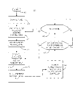
signal
is passed to an antenna 104 through a switch 108. Since modern receiver
designs
may operate over multiple bands, multiple transmitters and receivers may be
represented by transmitter 100 and receiver 112. Since the transmitter and
receiver share the same antenna, for each band of frequencies used by the
receiver, the design shown in FIG. 1 utilizes a separate filter 116, 120
through 124
(e.g., a SAW filter or the like) configured as notch filters. Switch 108
switches to
the correct notch filter for the band of transmitted signals based on commands
from
a control processor 130 based on a selected channel or band. These notch
filters
are used to prevent the relatively high power from the RF amplifier 134 of
transmitter 100 from entering the front end low noise amplifier of the
receiver 112
1
CA 02822138 2013-07-24
and either damaging the receiver or degrading operation thereof.
[0004] As worldwide radio receivers are developed, as many as 20 (or
possibly more) bands of frequencies may need to be accommodated to truly
handle
each possible frequency band.
[0005] BRIEF DESCRIPTION OF THE DRAWINGS
[0006] Example embodiments of the present disclosure will be described
below with reference to the included drawings such that like reference
numerals
refer to like elements and in which:
[0007] FIG. 1 is block diagram of an example full duplex radio design for
multiple frequency bands.
[0008] FIG. 2 is an exemplary implementation of a variable filter
arrangement consistent with certain embodiments of the present invention.
[0009] FIG. 3 is an exemplary implementation of a filter tuner circuit
consistent with certain embodiments of the present invention.
[0010] FIG. 4 is an example of a process flow for a filter tuning process
consistent with certain embodiments of the present invention.
DETAILED DESCRIPTION
[0011] The various examples presented herein outline methods, user
interfaces, and electronic devices that allow a multiple band radio to operate
without use of large numbers of individual filters for each of a plurality of
radio
bands.
[0012] For simplicity and clarity of illustration, reference numerals may
be
repeated among the figures to indicate corresponding or analogous elements.
Numerous details are set forth to provide an understanding of the embodiments
described herein. The embodiments may be practiced without these details. In
other instances, well-known methods, procedures, and components have not been
2
CA 02822138 2013-07-24
described in detail to avoid obscuring the embodiments described. The
description
is not to be considered as limited to the scope of the embodiments described
herein.
[0013] The terms "a" or "an", as used herein, are defined as one or more
than
one. The term "plurality", as used herein, is defined as two or more than two.
The
term "another", as used herein, is defined as at least a second or more. The
terms
"including" and/or "having", as used herein, are defined as comprising (i.e.,
open
language). The term "coupled", as used herein, is defined as connected,
although
not necessarily directly, and not necessarily mechanically. The term "program"
or
"computer program" or similar terms, as used herein, is defined as a sequence
of
instructions designed for execution on a computer system. A "program", or
"computer program", may include a subroutine, a function, a procedure, an
application or "app", an object method, an object implementation, in an
executable
application, an applet, a servlet, a source code, an object code, a script, a
program
module, a shared library / dynamic load library and/or other sequence of
instructions designed for execution on a computer system.
[0014] Therefore, in accordance with certain aspects of the present
disclosure, there is provided a radio transceiver having a transmitter and a
receiver.
A filter is coupled to an output of the transmitter, the filter having one or
more
integrated capacitors, where the filter is tuned by varying one or more
capacitance
values of the one or more integrated capacitors in the filter to tune the
filter, at
least one of the one or more integrated capacitors comprise Barium Strontium
Titanate (BST) ceramic integrated capacitors that are each tuneable by
application
of a bias voltage thereto. A filter tuner circuit is configured to apply the
bias
voltage to the one or more integrated capacitors, where the bias voltage is
initially
established as a stored initial value. A proportional-integral-derivative
(PID)
controller is configured to refine the bias voltage to optimize a power within
the
transceiver.
[0015] In certain implementations, the filter is a notch filter coupled
between
a transmitter output and a receiver input of the transceiver that blocks
transmitter
power from entering the receiver. In certain implementations, the ND
controller is
3
CA 02822138 2013-07-24
configured to maximize a difference between receiver frequency power and
transmitter frequency power at the receiver input. In certain implementations,
the
filter tuner circuit has a low pass filter configured to receive transmitter
signals
present at the receiver input, a power calculator configured to calculate
power
received from the low pass filter, and an error calculator configured to
calculate a
difference between the calculated power and receive frequency power present at
the receiver input, where the PID controller is configured to maximize a
difference
between the receiver frequency power and transmitter frequency power at the
receiver input. In certain implementations, the PID controller is configured
to
maximize a difference between receiver frequency power and transmitter
frequency
power at the receiver input. In certain implementations, the filter is a notch
filter.
[0016] In certain implementations, the transmitter and receiver described
above represent a plurality of transmitters and receivers operable over three
bands,
where the three bands comprise a low band between 700Mhz and 1Ghz, a middle
band between 1.8Ghz and 2.2Ghz and a high band between 2.3Ghz and 2.7Ghz. In
certain implementations, the filter described above represents three filters,
one for
each of the three bands, and where each of the three filters are coupled
directly to
one of three receivers. In certain implementations, the one or more integrated
capacitors are exposed to transmitter power in excess of 20dBm.
[0017] A radio transceiver consistent with certain implementations has a
multi-band transmitter and a multi-band receiver, where the transmitter and
receiver are configured to operate in full duplex with a transmitter channel
for use
by the transmitter and a receiver channel for use by the receiver. An antenna
is
shared by the transmitter and the receiver for full duplex communication,
where
the transmitter has an output coupled to the receiver and the receiver has an
input
coupled to the antenna. A notch filter made up of one or more integrated
capacitors is disposed between the antenna and the receiver. The notch filter
is
configured to be tuned by varying one or more capacitance values of the one or
more integrated capacitors in the notch filter to select the transmitter
channel for
rejection by the notch filter, at least one of the one or more integrated
capacitors
comprising Barium Strontium Titanate (BST) ceramic integrated capacitors that
are
4
CA 02822138 2013-07-24
each tuneable by application of a bias voltage thereto. A filter tuner circuit
is
configured to apply the bias voltage to the one or more integrated capacitors,
where the bias voltage is initially established as a stored initial value, and
where
the bias voltage is refined by a proportional-integral-derivative (PID)
controller
configured to optimize a power in the transceiver.
[0018] In certain implementations, the PID controller is configured to
maximize a difference between receiver frequency power and transmitter
frequency
power at the receiver input. In certain implementations, the filter tuner
circuit is a
low pass filter configured to receive transmitter signals present at the
receiver input
with a power calculator configured to calculate power received from the low
pass
filter, and an error calculator configured to calculate a difference between
the
calculated power and receive frequency power present at the receiver input,
where
the PID controller is configured to maximize a difference between receiver
frequency power and transmitter frequency power at the receiver input.
[0019] In certain implementations, the multi-band transmitter and multi-
band receiver described above represents a plurality of transmitters and
receivers
operable over three bands, where the three bands comprise a low band between
700Mhz and 1Ghz, a middle band between 1.8Ghz and 2.2Ghz and a high band
between 2.3Ghz and 2.7Ghz. Similarly, the filter described above represents
three
filters, one for each of the three bands, and where each of the three filters
are
coupled directly to one of three receivers. In certain implementations, the
one or
more integrated capacitors are exposed to transmitter power in excess of
20dBm.
[0020] An example method of tuning a filter in a radio transceiver,
involves
providing a tuneable filter forming a part of the transceiver having an
integrated
capacitor, where the integrated capacitor comprises as Barium Strontium
Titanate
(BST) ceramic integrated capacitor that is tuneable by application of a bias
voltage
thereto, where the transceiver has a transmitter and a receiver; retrieving a
stored
initial value of the bias voltage from a memory; and refining the initial
value of the
bias voltage by using a proportional-integral-derivative (PID) controller to
produce
CA 02822138 2013-07-24
a refined bias voltage and applying the refined value bias voltage to the
capacitor to
optimize a signal in the radio transceiver.
[0021] In certain implementations, the method further involves applying
the
initial value of the bias voltage to the capacitor prior to refining the
initial value. In
certain implementations, the refining comprises maximizing a difference
between a
power transmitted by the transmitter and a power from the transmitter
appearing
at the input of the receiver. In certain implementations, the filter comprises
a
notch filter coupled between a transmitter output and a receiver input of the
transceiver that blocks transmitter power from entering the receiver. In
certain
implementations, the refining comprises maximizing a difference between
receiver
frequency power and transmitter frequency power at the receiver input. In
certain
implementations, the transmitter and receiver comprise a plurality of
transmitters
and receivers operable over three bands, where the three bands comprise a low
band between 700Mhz and 1Ghz, a middle band between 1.8Ghz and 2.2Ghz and a
high band between 2.3Ghz and 2.7Ghz. In certain implementations, the filter
discussed above represents three filters, one for each of the three bands, and
where each of the three filters are coupled directly to one of three
receivers. In
certain implementations, the integrated capacitor is exposed to transmitter
power
in excess of 20dBm.
[0022] As noted above, as many as 20 bands of channels are to be
accommodated in order to provide a single radio that operates worldwide.
Unfortunately, the mechanism used in FIG. 1 for isolating the sensitive input
of the
receiver from high powers from the transmitter would result in use of a
complex
switch circuit 108 and perhaps twenty or more notch filters 116, 120 through
124.
Such filters while having a relatively small footprint individually, will
occupy a
considerable amount of space when twenty such filters are used. Moreover, the
cost of twenty filters increases the cost of the radio and constrains the how
small
the radio can be.
[0023] An improvement can be made by utilizing tuneable capacitors to
implement traditional inductor and capacitor filter structures. But simply
6
CA 02822138 2013-07-24
substituting LC filter designs that utilize conventional variable integrated
capacitors
may be detrimental to the life of the radio and may not conserve valuable real
estate. Conventional metal-insulator-metal (MIM) and metal-oxide-metal (MOM)
integrated capacitors may fail or degrade if exposed to high voltage and
power. For
example, such capacitors are generally limited to voltages of 3.0 volts
maximum to
achieve long term reliable performance. This corresponds to a maximum power of
about 13-14 dBm. But, 3G and 4G LTE cellular radio transmitters can output
between about 8 and 20 volts to provide output power in excess of 20 dBm and
generally between about 22 and 33 dBm. The filters may be exposed to such
powers in use for up to 5-10 years. Using conventional MIM and MOM integrated
capacitors to implement such filters will surely result in premature failure
or
performance degradation, and likely catastrophic failure of the radio.
[0024] In order to achieve a reasonable substitution of variable LC
filters in an
integrated radio system, conventional capacitors such as MIM capacitors or MOM
capacitors are clearly unsuitable. However, it has been found that doped
Barium
Strontium Titanate (BST) integrated ceramic capacitors such as those
manufactured
by Paratek Microwave, Inc. can reliably handle power in the range of 40 dBm
reliably for long periods of time. Additionally, in the present application,
twenty
bands of filters can be handled with only three variable filters for high,
middle and
low band frequency ranges. For current frequency allocations, this can be done
with a low band between 700Mhz and 1.0Ghz, a middle band of 1.86Ghz to 2.2Ghz
and a high band between 2.3Ghz and 2.7Ghz, with each band handling six to
seven
channels.
[0025] In the present case, this means that only three variable
integrated
variable capacitor based filters can be used to replace twenty fixed filters.
Since
suitable BST based filters designs occupy approximately the same footprint as
a
single fixed SAW filter, the size savings within the radio are substantial
(3/20=0.15
for approximately an 85% savings). Additionally, since a separate receiver is
used
for each of the three bands (high, low and middle) the switch can be
eliminated by
simply attaching the variable filter to the front end of each of the three
receivers.
Thus, each variable filter is paired with a radio receiver of the same band.
Any
7
CA 02822138 2013-07-24
suitable notch filter design, for the present implementation, can be utilized.
[0026] An example receiver has the following elements: The receiver is
coupled to the output of the transmitter (i.e. near the antenna) via a
coupler. This
then goes through a tuneable LC (inductive-capacitive) tank that uses BST
tuneable
integrated capacitors. This is followed by the receiver pre-amp or attenuator,
and
then a mixer that is attached to a voltage controlled oscillator (VCO) and
phase
locked loop (PLL). The VCO uses an oscillator that has high frequency
protection on
the supplies and grounds. After the mixer, filtering and automatic gain
control
(AGC) follow and then a high band width low current analog to digital
converter
(ADC) (for example a 100MHz SAR ADC). The output of ADC are then applied to
the various digital signal processing (DSP) blocks for either envelope
tracking,
antenna tuning, or detecting the contents of the RX spectrum.
[0027] FIG. 2 is a simplified illustration of an example electronic
device 200
in accordance with aspects of the present disclosure. In this example radio,
the
bank of filters depicted in FIG. 1 is replaced with one or more variable
filters 204.
These variable notch filters 204 are coupled directly to the input RF
amplifier (i.e.,
the "front end") 208 of the receivers 210 in accord with certain
implementations
(only one band shown for simplicity and ease of illustration, but it will be
understood that multiple filters and receivers are utilized to cover all
twenty bands).
The variable LC filter 204 is configured as any desired LC notch filter
circuit in this
application so that power from the transmitter 206's output power amplifier
212
which is intended for antenna 216 is largely blocked from the input of
receiver RF
amplifier 208. The RF amplifier 208 is coupled to the remainder of the
receiver
which is shown in part by mixer 220 (which mixes the incoming receiver channel
signal with the receiver frequency FRF for direct conversion to baseband) and
ADC
224 for operation in a more or less conventional manner which need not be
discussed in detail for purposes of this discussion.
[0028] The signal at the receiver input is also utilized to control the
tuning of
the variable integrated capacitor or capacitors used in the LC filter 204 by
amplifying the signal using RF amplifier 230 to condition the signal to a
suitable
8
CA 02822138 2013-07-24
level for mixing at mixer 234 with the receiver frequency using a local
oscillator at
the transmitter frequency F-rx. Hence, signals at the receive frequency and
the
transmit frequency are available for measurement and calculation of
adjustments
for the filter 204 using the filter tuner 250.
[0029] In order to implement a suitable filter controller 250, the filter
controller is designed and configured so that the adjusted frequency of the
filter is
manipulated such that the transmit signal is effectively notched out. In this
example implementation, a proportional-integral-derivative (PID) controller is
chosen to do this. Since the carrier frequency of the transmitter is known by
virtue
of the channel selection mechanism of the radio, this information can be used
to
initially coarsely tune the capacitor(s) of the LC filter(s) 204. The PID
controller can
then be used in a feedback loop as shown with the filter tuner 250 feeding
back
control signals to LC filter 204 to adjust the capacitor values to achieve an
optimized tuning. Any suitable optimization technique can be utilized by the
PID
controller without limitation.
[0030] FIG. 3 is a block diagram of an example functional representation
of
the filter tuner 250. In accord with this example filter tuner 250, the
baseband
transmit signal is low pass filtered to eliminate mixing artefacts at filter
304. This
filtered baseband transmit signal is passed to a power calculator block 308
that
calculates the power in the residual transmit signal present at the input of
the
receiver. This calculated power is then sent to error calculator 312 that
compares
this power to a reference value and the output is provided to a PID controller
318
for processing. The initial value or values used to initially set the filter's
tuning is
stored in memory 324 and that value is initially loaded into the LC filter 204
when
the channel is selected. The PID controller modifies this value iteratively to
minimize the amount of power from the transmitter that is received at the
receiver.
In one example implementation, this can be effectively accomplished by
maximizing
the difference between receiver frequency power PRx and transmit frequency
power
P-rx at the receiver input (i.e., RX-=TX,/ MAX(P P 11, where in this
example, the reference
=
value provided to the error calculator is the receive frequency power. This
maximization process accounts for any effects the notch filter has on the
receive
9
CA 02822138 2013-07-24
frequency power as well as the transmit frequency power.
[0031] In the present example implementation, any number of filter tuner
implementations can be utilized. FIG. 4 depicts one example implementation
process 400 starting at 402. When a channel is tuned at 406, by any suitable
mechanism, initial filter values may be loaded into the tuneable LC filter 204
at
410. These initial values may be factory generated as approximate values for a
given design, or may be measured and stored for a particular production radio.
Even if the initial value is selected for an individual production radio, the
RF filter
based on inductors and capacitors values will desirably be tuned to optimize
the
filter characteristics since given components will drift in values with age,
changes in
temperature, etc. Once the filter has been adjusted according to the present
process, the value used most recently may be stored as a new initial value on
a
channel by channel basis or the original default may be used each time without
limitation.
[0032] The transmit frequency signal at the receiver input is low pass
filtered
to remove the unneeded mixing components at 414 and the transmit power at the
receiver input is calculated from the signal at 418. The error from the
reference
values (the receiver power signal) is calculated at 422 and a correction
factor is
computed at 426 using the PID controller in order to optimize the power
difference
between the receiver and transmit power at 430. The calculation of a
correction
factor is iterated in the loop made up of 418, 422, 426 and 430 until the
filter value
is optimized at 430. Once this correction factor is optimized it may be
monitored
periodically or simply left in place at 430. This process repeats itself
starting at 410
whenever a new channel is selected at 440.
[0033] Those skilled in the art will appreciate that this process may be
interrupted during the optimizing process should a channel change be effected
prior
to full optimization, but the basic process can be understood by reference to
the
process 400 for illustrative purposes. Other variations will occur to those
skilled in
the art upon consideration of the present teachings. For example, the
optimization
can be carried out by minimizing the transmit power at the receiver input or
by
CA 02822138 2013-07-24
other techniques than those depicted herein without departing from embodiments
consistent with the present invention.
[0034] The order in which the optional operations represented in the flow
chart 400 may occur in any operative order without limitation. Thus, while the
blocks comprising the methods are shown as occurring in a particular order, it
will
be appreciated by those skilled in the art that certain of the blocks may be
rearranged and can occur in different orders and be augmented by other process
functions than those shown without materially affecting the end results of the
methods.
[0035] The implementations of the present disclosure described above are
intended to be examples only. Those of skill in the art can effect
alterations,
modifications and variations to the particular example embodiments herein
without
departing from the intended scope of the present disclosure. Moreover,
selected
features from one or more of the above-described example embodiments can be
combined to create alternative example embodiments not explicitly described
herein. For example, while the embodiment discussed above utilizes a notch
filter
that prevents excessive transmitter power from entering the receiver, other
example implementations could use a band pass, low pass or high pass filter
configuration where tuning of the filter is accomplished by optimization of a
power
or power difference (both referred to herein as a power).
[0036] It will be appreciated that any module or component disclosed
herein
that executes instructions may include or otherwise have access to non-
transitory
and tangible computer readable media such as storage media, computer storage
media, or data storage devices (removable or non-removable) such as, for
example, magnetic disks, optical disks, or tape data storage. In this
document, the
term "non-transitory" is only intended to exclude propagating waves and
signals
and does not exclude volatile memory or memory that can be rewritten or
erased.
Computer storage media may include volatile and non-volatile, removable and
non-
removable media implemented in any method or technology for storage of
information, such as computer readable instructions, data structures, program
11
CA 02822138 2015-03-09
modules, or other data. Examples of computer storage media include random
access memory (RAM), read only memory ROM, electrically erasable programmable
read only memory (EEPROM), flash memory or other memory technology, compact
disc ROM (CD-ROM), digital versatile disks (DVD) or other optical storage,
magnetic
cassettes, magnetic tape, magnetic disk storage or other magnetic storage
devices,
or any other medium which can be used to store the desired information and
which
can be accessed by an application, module, or both. Any such computer storage
media may be part of the server, any component of or related to the network,
backend, etc., or accessible or connectable thereto. Any application or module
herein described may be implemented using computer readable/executable
instructions that may be stored or otherwise held by such computer readable
media.
[0037] The present disclosure may be embodied in other specific forms
without departing from its essential characteristics. The described
embodiments
are to be considered in all respects only as illustrative and not restrictive.
The
scope of the disclosure is, therefore, indicated by the appended claims rather
than
by the foregoing description. All changes that come within the meaning and
range
of equivalency of the claims are to be embraced within their scope.
[0038] What is claimed is:
12