Note: Descriptions are shown in the official language in which they were submitted.
CA 02823254 2013-06-27
WO 2012/092209 PCT/US2011/067258
WIRELESSS ENERGY SOURCES FOR INTEGRATED CIRCUITS
INTRODUCTION
[001] Pursuant to 35 U.S.C. 119 (e), this application claims priority to the
filing date
of United States Provisional Patent Application Serial No. 61/428,055 entitled
WIRELESS ENERGY SOURCES FOR INTEGRATED CIRCUITS filed November
29, 2010, the disclosure of which applications is herein incorporated by
reference.
[002] The present disclosure is related generally to wireless energy sources
for
integrated circuits. More particularly, the present disclosure is related to
wireless
energy sources comprising energy harvesting and power management circuits for
wireless power delivery to ingestible identifiers comprising an integrated
circuit.
[003] In the context of ingestible identifiers, such as an ingestible event
marker (I EM),
prescription medications are effective remedies for many patients when taken
properly, e.g., according to instructions. Studies have shown, however, that
on
average, about 50% of patients do not comply with prescribed medication
regimens.
A low rate of compliance with medication regimens results in a large number of
hospitalizations and admissions to nursing homes every year. In the United
States
alone, it has recently been estimated that the healthcare related costs
resulting from
patient non-compliance is reaching $100 billion annually.
[004] Consequently, identifiers generally referred to as event markers have
been
developed, which may be incorporated into pharma-informatics enabled
pharmaceutical compositions. These devices are ingestible and/or digestible or
partially digestible. Ingestible devices include electronic circuitry for use
in a variety
of different medical applications, including both diagnostic and therapeutic
applications. Some ingestible devices such as I EMs made by Proteus
Biomedical,
Inc., Redwood City, California, typically do not require an internal energy
source for
operation. The energy sources for these I EMs are activated upon association
with a
target site of a body by the presence of a predetermined specific stimulus at
the
target site, e.g., liquid (wetting), time, pH, ionic strength, conductivity,
presence of
biological molecules (e.g., specific proteins or enzymes that are present in
the
stomach, small intestine, colon), blood, temperature, specific auxiliary
agents (foods
1
CA 02823254 2013-06-27
WO 2012/092209 PCT/US2011/067258
ingredients such as fat, salt, or sugar, or other pharmaceuticals whose co-
presence
is clinically relevant), bacteria in the stomach, pressure, light. The
predetermined
specific stimulus is a known stimulus for which the controlled activation
identifier is
designed or configured to respond by activation.
[005] A communication broadcasted by the energized ingestible identifier may
be
received by another device, e.g., a receiver, either inside or near the body,
which
may then record that the identifier, e.g., one that is associated with one or
more
active agents and pharmaceutical composition, has in fact reached the target
site.
[006] The digestibility or partial digestibility of the internal energy source
and circuitry
make it difficult to run diagnostic tests on the circuitry or other components
without
energizing the ingestible identifier and/or dissolving the device and thus
deploying
and/or destroying it prior to its ultimate end use. Therefore, it would be
advantageous to provide a wireless energy source to energize ingestible
identifier
systems in a wireless mode and carry out diagnostic tests and verify
operation,
presence, and/or functionality of the ingestible identifier prior to its
ultimate use.
SUMMARY
[007] In one aspect, a system comprises a control device and a wireless energy
source
electrically coupled to the control device. The wireless energy source
comprises an
energy harvester to receive energy at an input thereof in one form and to
convert the
energy into a voltage potential difference to energize the control device.
[008] In another aspect, a system comprises a control device for altering
conductance,
a wireless energy source electrically coupled to the control device, and a
partial
power source. The wireless energy source comprises an energy harvester to
receive energy at an input thereof in one form and to convert the energy into
a first
voltage potential difference to energize the control device. The partial power
source
comprises a first material electrically coupled to the control device and a
second
material electrically coupled to the control device and electrically isolated
from the
first material. The first and second materials are selected to provide a
second
voltage potential difference when in contact with a conducting liquid. The
control
2
CA 02823254 2013-06-27
WO 2012/092209 PCT/US2011/067258
device alters the conductance between the first and second materials such that
the
magnitude of the current flow is varied to encode information.
[009] In yet another aspect, a system comprises a control device, a wireless
energy
source electrically coupled to the control device and a power source
electrically
coupled to the control device. The wireless energy source comprises an energy
harvester to receive energy at an input thereof in one form and to convert the
energy
into a first voltage potential difference to energize the control device. The
power
source is electrically coupled to the control device and provides a second
voltage
potential difference to the control device.
FIGURES
[010] FIG. 1 illustrates one aspect of a system comprising a wireless energy
source
and an identifier system for indicating the occurrence of an event.
[011] FIG. 2 illustrates one aspect of a system comprising a wireless energy
source,
similar to the wireless energy source of FIG. 1, and an identifier system for
indicating
the occurrence of an event.
[012] FIG. 3 illustrates one aspect of a system comprising a wireless energy
source,
similar to the wireless energy sources of FIGS. 1 and 2, and an identifier
system for
indicating the occurrence of an event.
[013] FIG. 4 illustrates one aspect of a wireless energy source comprising an
energy
harvester and a power management circuit configured to harvest electromagnetic
energy from the environment in the form of optical radiation.
[014] FIG. 5 illustrates one aspect of a system that employs an energy
harvesting
technique based on optical radiation.
[015] FIG. 6 illustrates one aspect of a system that employs an energy
harvesting
technique based on modulated optical radiation.
[016] FIG. 7 is a schematic diagram of a vibration/motion system that may be
employed in vibration energy harvester described herein in connection with
FIGS. 8-
11.
3
CA 02823254 2013-06-27
WO 2012/092209 PCT/US2011/067258
[017] FIG. 8 illustrates one aspect of a system comprising a wireless energy
source
that comprises an energy harvester comprising an electrostatic energy
conversion
element to convert vibration/motion energy into electrical energy as described
in
connection with FIG. 7.
[018] FIG. 9 illustrates one aspect of a system comprising a wireless energy
source
that comprises an energy harvester comprising a piezoelectric energy
conversion
element to convert vibration/motion energy into electrical energy as described
in
connection with FIG. 7.
[019] FIG. 10 is a schematic diagram of a piezoelectric type capacitor element
of a
wireless energy source that is configured to operate on the vibration/motion
energy
harvesting principle described in FIG. 7.
[020] FIG. 11 illustrates one aspect of a system comprising a wireless energy
source
that comprises an energy harvester comprising an electromagnetic energy
conversion element to convert vibration/motion energy into electrical energy
as
described in connection with FIG. 7.
[021] FIG. 12 illustrates one aspect of a system comprising a wireless energy
source
that comprises an energy harvester comprising an acoustic energy conversion
element.
[022] FIG. 13 illustrates one aspect of a system comprising a wireless energy
source
comprising an energy harvester comprising a radio frequency energy conversion
element.
[023] FIG. 14 illustrates one aspect of a system comprising a wireless energy
source
comprising an energy harvester comprising a thermoelectric energy conversion
element.
[024] FIG. 15 illustrates one aspect of a system comprising a wireless energy
source
comprising an energy harvester comprising a thermoelectric energy conversion
element similar to the element discussed in connection with FIG. 14.
[025] FIG. 16 illustrates one aspect of an ingestible product that comprises a
system
for indicating the occurrence of an event is shown inside the body.
4
CA 02823254 2013-06-27
WO 2012/092209 PCT/US2011/067258
[026] FIG. 17A illustrates a pharmaceutical product shown with a system, such
as an
ingestible event marker or an ionic emission module.
[027] FIG. 17B illustrates a pharmaceutical product, similar to the product of
FIG. 17A,
shown with a system, such as an ingestible event marker or an identifiable
emission
module.
[028] FIG. 18 illustrates a more detailed diagram of one aspect of the systems
of FIGS.
17A and 17B.
[029] FIG. 19 illustrates one aspect of a system comprising a sensor and in
contact
with the conducting fluid.
[030] FIG. 20 is a block diagram representation of a device described in
connection
with FIGS. 18 and 19.
[031] FIG. 21 illustrates another aspect of the systems of FIGS. 17A and 17B,
respectively, shown in more detail as system.
[032] FIG. 22 illustrates one aspect of a system, similar to the system of
FIG. 18, which
includes a pH sensor module connected to a material, which is selected in
accordance with the specific type of sensing function being performed.
[033] FIG. 23 is a schematic diagram of a pharmaceutical product supply chain
management system.
[034] FIG. 24 is schematic diagram of a circuit that may be representative of
various
aspects.
DESCRIPTION
[035] The present disclosure provides multiple aspects of systems comprising a
wireless energy source for energizing identifiers to indicate the occurrence
of an
event. In addition, the system may include other energy sources and may be
activated in multiple other modes as described below. In one aspect, the
wireless
energy source may be activated in a wireless mode by an external source. In
another aspect, in addition, the system may be activated in a galvanic mode by
a
chemical reaction by exposing the system to a conducting fluid.
CA 02823254 2013-06-27
WO 2012/092209 PCT/US2011/067258
[036] In the wireless activation mode, the identifier system may be activated
by a
stimulus from an external and/or an internal source for example, an
Implantable
Pulse Generator (IPG). The stimulus provides energy that can be harvested by
the
wireless energy source. The external stimulus may be provided by
electromagnetic
radiation in the form of light or radio frequency (RF), vibration, motion,
and/or
thermal sources. In response to the stimulus, the system is energized and
generates a signal that can be detected by external and/or internal devices in
order
to communicate information associated with the system to such devices. In one
aspect, the system is operative to communicate information that can be used to
conduct diagnostic tests on, verify operation of, detect presence of, and/or
determine
the functionality of the system. In other aspects, the system is operative to
communicate a unique current signature associated with the system.
[037] In the galvanic activation mode, the system is activated when it comes
into
contact with a conducting fluid. In the instance where the system is used with
a
product intended to be ingested by a living organism, upon ingestion, the
system
comes into contact with a conducting body fluid and is activated. In one
aspect, the
system includes dissimilar materials positioned on a framework such that when
a
conducting fluid comes into contact with the dissimilar materials, a voltage
potential
difference is created. The voltage potential difference, and hence the
voltage, is
used to energize or power up control logic that is positioned within the
framework.
The potential difference causes ions or current to flow from the first
dissimilar
material to the second dissimilar material via the control logic and then
through the
conducting fluid to complete a circuit. The control logic is operative to
control the
conductance between the two dissimilar materials and, hence, controls or
modulates
the conductance. In addition, the control logic is capable of encoding
information on
a current signature.
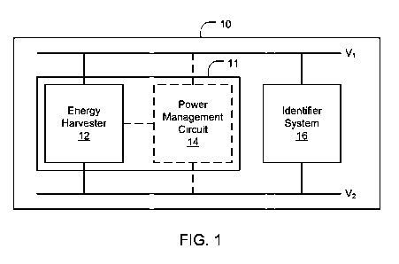
[038] FIG. 1 illustrates one aspect of a system 10 comprising a wireless
energy source
11 and an identifier system 16 comprising a control device for indicating the
occurrence of an event. The wireless energy source 11 energizes the control
device
in a wireless mode. The wireless energy source 11 comprises an energy
harvester
12 to convert energy in one form received at an input thereof to energy in
another
6
CA 02823254 2013-06-27
WO 2012/092209 PCT/US2011/067258
form at an output thereof. In various aspects, the output energy is in the
form of a
voltage potential difference. Optionally, the wireless energy source may
comprise a
power management circuit 14 (shown in phantom to indicate that it is optional)
for
providing energy suitable to operate the circuits of the identifier system 16.
In one
aspect, the system 10 may be a tag, such as an electronic label associated
with an
article for the purpose of identifying the article, for example. The system 10
can be
used in a variety of different applications, including as a component of an
ingestible
identifier, such as an IEM, e.g., pharma-informatics enabled pharmaceutical
composition. In one aspect, the identifier system 16 comprises an in-body
device
that is operative when energized to communicate information to an external
system
located outside the body. In one aspect, the in-body device is operative to
communicate information outside the body only when the wireless energy source
is
energized by an external energy source located outside the body.
[039] In the most general aspect referenced in FIG. 1, the system 10 does not
contain
a standalone internal energy source, such as a partial power supply (described
hereinbelow), battery, or supercapacitor, for example, and is powered solely
by a
voltage potential (V1-V2) generated by the wireless energy source 11 from the
energy collected by the energy harvester 12 as disclosed herein.
[040] In various aspects, described in more detail below, the energy harvester
12
collects energy from the environment using a variety of techniques including,
but not
limited to, electromagnetic radiation (e.g., light or RF radiation),
vibrations/motion,
acoustic waves, thermal. Such techniques may be implemented using a variety of
technologies, such as, for example, micro-electro mechanical systems (MEMS),
electromagnetic, piezoelectric, thermoelectric (e.g., Seebeck or Peltier
effects),
among others. The energy harvester 12 may be optimized to accommodate the
particular energy harvesting technique implemented by the system 10.
[041] In some aspects, the input to the energy harvester 12 can be driven or
stimulated
directly by a dedicated source to produce direct current power source, such as
a
battery in the form of a voltage potential suitable to operate the circuits of
the
identifier system 16 at the output of the energy harvester 12. In such
aspects, the
7
CA 02823254 2013-06-27
WO 2012/092209 PCT/US2011/067258
power management circuit 14 may be eliminated. In other aspects, when the
voltage potential developed by the energy harvester 12 is not suitable to
operate the
circuits of the identifier system 16, the power management circuit 14 may
employed
to provide a voltage potential that is suitable for powering the circuits of
the identifier
system 16. The power management circuit 14 can adapt its input to the energy
harvester 12 implemented by the system 10 and its output to the load, e.g.,
the
identifier system 16. In various aspects, the power management circuit 14 may
comprise some form of converter to convert the input voltage generated by the
energy harvester 12 to a voltage potential suitable for operating the
identifier system
16. Although the converter may be implemented in different configurations, DC-
DC
converters, charge pumps, boost converters, and rectifying AC-DC converters
may
be adapted for use in the power management circuit 14. Additionally, the power
management circuit 14 may comprise voltage regulator, buffer, and control
circuits,
among others.
[042] In one aspect, either the system 10 and/or the identifier system 16 may
be
fabricated on an integrated circuit (IC). In certain aspects, the identifier
system 16
may comprise an on-board random access memory (RAM). The identifier system 16
comprises control logic that is operative to modulate the voltage on a
capacitor plate
located on a top surface of the IC with respect to the substrate voltage of
the IC to
modulate the information to be communicated. The modulated voltage can be
detected by a capacitively coupled reader (not shown). Accordingly, when the
wireless energy source 11 is activated by an external source, the identifier
system
16 is operative to communicate information associated with the system 10. The
information may be employed to functionally test and perform diagnostic tests
on the
system 10 as well as verify the operation of and detect the presence of the
system
10. In other aspects, the identifier system 16 is operative to communicate a
unique
signature associated with the system 10.
[043] Although described generally herein in terms of voltage potential, the
scope of
the disclosed systems is not so limited. In that regard, where the operation
of the
circuits of the identifier system 16 depend on the delivery of a predetermined
current
8
CA 02823254 2013-06-27
WO 2012/092209 PCT/US2011/067258
rather than a predetermined voltage potential, the energy harvester 12 and/or
power
management circuit 14 may be designed and implemented to operate accordingly.
[044] FIG. 2 illustrates one aspect of a system 20 comprising a wireless
energy source
21, similar to the wireless energy source 11 of FIG. 1, and an identifier
system 22 for
indicating the occurrence of an event. The wireless energy source 21 energizes
the
control device in a wireless mode. The wireless energy source 21 comprises an
energy harvester 12 to convert energy in one form received at an input thereof
to
energy in another form at an output thereof. In various aspects, the output
energy is
in the form of a voltage potential difference. Optionally, the wireless energy
source
may comprise a power management circuit 14 (shown in phantom to indicate that
it
is optional) for providing energy suitable to operate the circuits of the
identifier
system 16. In the referenced aspect, the system 20 comprises a hybrid energy
source comprising the wireless energy source 11 and a partial power source in
the
identifier system 22. The wireless energy source 11 is electrically coupled to
the
control device 24 to supply power to the circuits of the identifier system 22
separately from the partial power source. In one aspect, the partial power
source
can be activated in galvanic mode when it comes into contact with a conductive
fluid,
which may comprise a conductive liquid, gas, mist, or any combination thereof.
The
wireless energy source 11 and the partial power source may be activated either
individually or in combination. Accordingly, the system 20 may be operated in
a
wireless mode, a galvanic mode, or combinations thereof. The system 20 can be
used in a variety of different applications, including as a component of an
ingestible
identifier, such as an IEM, e.g., pharma-informatics enabled pharmaceutical
composition.
[045] The identifier system 22 comprises a control device 24 for altering
conductance
and a partial power source comprising a first conductive material 26
electrically
coupled to the control device 24 and a second conductive material 28
electrically
coupled to the control device and electrically isolated from the first
material 26. The
first and second conductive materials 26, 28 are selected to provide a voltage
potential difference when in contact with a conducting fluid. The control
device 24
alters the conductance between the first and second conductive materials 26,
28
9
CA 02823254 2013-06-27
WO 2012/092209 PCT/US2011/067258
such that the magnitude of the current flow is varied to encode information.
As
discussed in reference to FIG. 1, optionally the power management circuit 14
may
be employed to adapt its input to the energy harvester 12 and its output to
the load,
e.g., the identifier system 22. The control device 24 comprises control logic
that is
operative in either wireless or galvanic modes to modulate the voltage on the
first
and second conductive materials 26, 28 to communicate information. The
modulated voltage can be detected by respective first and second capacitively
coupled plates of a reader positioned externally of the system 20. In one
aspect, the
system 20 may comprise additional capacitive plates formed of similar or
dissimilar
conductive materials operative to communicate information associated with the
system 20.
[046] FIG. 3 illustrates one aspect of a system 30 comprising a wireless
energy source
31, similar to the wireless energy sources 11, 21 of FIGS. 1 and 2, and an
identifier
system 32 for indicating the occurrence of an event. The wireless energy
source 31
energizes the control device in a wireless mode. The wireless energy source 31
comprises an energy harvester 12 to convert energy in one form received at an
input
thereof to energy in another form at an output thereof. In various aspects,
the output
energy is in the form of a voltage potential difference. Optionally, the
wireless
energy source may comprise a power management circuit 14 (shown in phantom to
indicate that it is optional) for providing energy suitable to operate the
circuits of the
identifier system 16. The system 30 can be used in a variety of different
applications, including as a component of an ingestible identifier, such as an
IEM,
e.g., pharma-informatics enabled pharmaceutical composition.
[047] In the referenced aspect, the system 30 comprises a hybrid energy source
comprising the wireless energy source 31 and an on-board power source 35 such
as
a micro-battery or supercapacitor. The wireless energy source 31 is coupled to
the
on-board power source 35 and can be employed to power the identifier system 30
in
the wireless mode. In one aspect, the micro-battery may be a thin film
integrated
battery fabricated directly in IC packages in any shape or size. In another
aspect, a
thin-film rechargeable battery or a supercapacitor may be designed and
implemented to bridge the gap between a battery and a conventional capacitor.
In
CA 02823254 2013-06-27
WO 2012/092209 PCT/US2011/067258
design implementations incorporating a rechargeable thin-film micro-battery or
supercapacitor, the wireless energy source 31 may be employed for charging or
recharging the battery or supercapacitor. Thus, the wireless energy source 31
can
be employed to minimize energy drain of the on-board power source 35.
[048] The identifier system 32 comprises a control device 34 for altering
conductance
and a partial power source comprising a first capacitive plate 36 electrically
coupled
to the control device 34 and a second capacitive plate 38 electrically coupled
to the
control device and electrically isolated from the first capacitive plate 36.
The control
device 34 alters the conductance between the first and second capacitive
plates 36,
38 such that the magnitude of the current flow is varied to encode
information. The
wireless energy source 31 is coupled to the control device 34 to supply power
to the
circuits of identifier system 32 separately from or in conjunction with the on-
board
power source 35. As discussed in reference to FIGS. 1 and 2, optionally the
input of
the power management circuit 14 may be adapted to the output of the energy
harvester 12 and the output of the power management circuit 14 may be adapted
to
the load, e.g., the identifier system 32. The control device 34 comprises
control logic
that is operative to modulate a voltage on the first and second conductive
plates 36,
38 to modulate the information to be communicated. The voltage modulated onto
the first and second conductive plates 36, 38 can be detected by respective
first and
second capacitively coupled plates of a reader. The first and second
capacitive
plates 36, 38 may be formed of similar or dissimilar materials.
[049] In the aspects referenced in FIGS. 1-3, the power management circuit 14
is
shown in phantom to indicate that it may be optional. The power management
circuit 14 may be employed to regulate, boost, or condition the energy
collected by
the energy harvester 12 to provide a direct current power source, such as a
battery,
in the form of a voltage potential suitable for operating the circuits of the
systems 16,
22, 32. It will be appreciated that any of the components or elements of the
systems
16, 22, 32 can be used alone or in combination in other systems within the
scope of
the present disclosure.
11
CA 02823254 2013-06-27
WO 2012/092209 PCT/US2011/067258
[050] In the various aspects of the systems 10, 20, 30 described in connection
with
FIGS. 1-3, the energy harvester 12, power management circuit 14, and circuits
of
the identifier systems 16, 22, 32 can be integrated in a one or multiple ICs.
In
operation, when activated in either in wireless or galvanic mode, the systems
10, 20,
30 are operable to indicate the occurrence of an event. Although different
modes of
communication may be employed, the information communicated may be the same.
In the wireless mode, the information may be communicated as a series of
pulses at
a rate of 10-20 Hz and may be phase modulated at 1kHz. The information may be
encoded using a variety of techniques such as Binary Phase-Shift Keying
(BPSK),
Frequency Modulation (FM), Amplitude Modulation (AM), On-Off Keying, and PSK
with On-Off keying. In certain aspects, the systems 10, 20, 30 and/or
identifier
systems 16, 22, 32 may comprise an on-board RAM. The information may comprise
identification number, information contained in the on-board RAM such as
medication, date code, and manufacturing date. In one aspect, the information
may
be communicated by modulating a voltage on a plate formed on a top surface of
the
IC with respect to the substrate voltage of the IC. A capacitively coupled
reader can
be used to detect the modulated voltage (shown in FIGS. 23, 24, for example).
[051] Furthermore, any of the identifier systems 16, 22, 32 described in
connection
with respective FIGS. 1-3 can be implemented to include an in-body device such
as
an I EM that can be energized in multiple modes and communicate information
outside the body using multiple techniques. By way of example and not
limitation, in
one aspect the I EM may be energized by deriving external (outside the body)
potentials and internal (inside the body) potentials at different points in
time and
responding to such external and internal potentials by communicating to at
least one
external device located inside or partially inside or outside the body. In
another
aspect, the I EM may derive different levels of potentials through external
and
internal energizing elements (e.g., energy harvester comprising a wireless
energy
source, an internal galvanic energy system, a micro-battery, or
supercapacitor) and
communicating to an external device in response to such derived different
levels of
potentials. In another aspect, the I EM may derive energy from an external
source
and store the derived energy in a capacitor or supercapacitor, for example,
where
12
CA 02823254 2013-06-27
WO 2012/092209 PCT/US2011/067258
the IEM can employ the stored energy for communicating to an external device
after
a delay. In yet another aspect, the IEM can be energized by external or
internal
sources at different locations within the body such as, for example,
esophagus,
stomach, lower part of the intestine, colon, and so forth. In another aspect,
the IEM
may employ external and internal energy selectively to communicate to
different
external devices at different points in time. In various aspects, the IEM may
communicate with different external devices e.g., a patch or other receivers
placed
in watches, necklaces or external locations. Examples of external devices that
the
IEM may communicate with are described in commonly assigned U.S. Patent
Application Publication No. 201 0/031 21 88 (Serial No. 12/673326) filed
December
15, 2009 and entitled "Body-Associated Receiver and Method," U.S. Patent
Application Publication Number 2008/0284599 (Serial No. 11/912475) filed April
28,
2006 entitled "Pharma-Informatics System," and U.S. Patent Application
Publication
Number 2009/0227204 (Serial No. 12/404184) filed March 13, 2009 entitled
"Pharma-Informatics System," where the disclosure of each is incorporated
herein
by reference in its entirety. In yet another aspect, the IEM may only receive
a
control command for its activation from any external and/ or internal device
while the
IEM is energized by any of the modes discussed above.
[052] FIG. 4 illustrates one aspect of a wireless energy source 41 comprising
an
energy harvester 12 and a power management circuit 14 configured to harvest
electromagnetic energy from the environment in the form of optical radiation.
The
energy harvester 12 comprises an optical energy conversion element such as a
photodiode 42 configured to convert incoming radiant electromagnetic energy in
the
form of light 44 photons into electrical energy. The particular photodiode 42
may be
selected to optimally respond to the wavelength of the incoming light 44,
which can
range from the visible spectrum to the invisible spectrum. As used herein the
term
radiant electromagnetic energy refers to light in the visible or invisible
spectrum
ranging from the ultraviolet to the infrared frequency range.
[053] As shown in FIG. 4, as light 44 strikes the P-N junction of the
photodiode 42,
either a current or voltage is generated by the photodiode 42 depending on the
mode of operation. In the referenced aspect, the photodiode 42 is reverse
biased
13
CA 02823254 2013-06-27
WO 2012/092209 PCT/US2011/067258
and a current i proportional to the amount of light 44 striking the photodiode
42 flows
from the photodiode 42 into a charge pump 46 circuit. The charge pump 46 may
be
implemented in a variety of configurations. Essentially, a charge pump is a
type of
DC-DC converter that uses capacitors as energy storage elements to create a
higher (boost) voltage power source. The charge pump 46 circuits are
relatively
simple and are capable of high efficiencies - as high as 90-95%, making them
attractive solutions for voltage boosting applications.
[054] The charge pump 46 uses some form of switching device(s) to control the
connection of voltages to the capacitors. To generate a higher voltage, a
first stage
involves connecting a capacitor across a voltage to charge it up. In a second
stage,
the capacitor is disconnected from the original charging voltage and
reconnected
with its negative terminal to the original positive charging voltage. Because
the
capacitor retains the voltage stored across it (ignoring leakage effects) the
positive
terminal voltage is added to the original, effectively doubling the voltage.
The
pulsing nature of the higher voltage output can be typically smoothed by the
use of
an output capacitor. Accordingly, the charge pump 46 converts the current i
generated by the photodiode 42 into an output voltage v0. The charge pump 46
may
have any suitable number of stages to boost the input voltage to any suitable
level.
A control circuit 49 controls the operation of the switching device(s) to
coordinate the
connection of voltages to the capacitors of the charge pump 46 to generate an
output voltage v, suitable to operate the circuits of the identifier systems
16, 22, 32
of FIGS. 1-3.
[055] DC-DC converters can be either boost converters or charge pumps. For
high
efficiency, most conventional DC-DC converters employ an external inductor.
Because large value inductors with many windings are difficult to fabricate
using a
monolithic or planar micro-fabrication process, charge pumps are more readily
suited in integrated circuit implementations because capacitors are used
rather than
inductors. This enables efficient DC-DC conversion. There exist many
alternative
configurations for DC-DC converters using switching capacitors. Such DC-DC
converters include, without limitation, voltage doublers, the Dickson charge
pump,
the ring converter, and the Fibonacci converter, among others.
14
CA 02823254 2013-06-27
WO 2012/092209 PCT/US2011/067258
[056] A voltage regulator 48 may optionally be coupled to the charge pump 46.
The
voltage regulator regulates the output voltage v, of the charge pump 46 and
produces a regulated output voltage V1 relative to a substrate voltage V2. The
voltage potential (V1-V2) is suitable to operate the circuits of any of the
systems 16,
22, 32 of FIGS. 1-3. In various aspects, the charge pump 46 may be replaced
with
any suitable voltage boosting circuit such as boost regulator, flyback, step-
up
(boost), or forward converter. In other aspects, the charge pump 46 may be
replaced with a DC-DC converter type voltage boosting circuit.
[057] In one aspect, the photodiode 42 may be a conventional photodiode, PIN
photodiode, or Complementary Metal Oxide Semiconductor (CMOS) PN diode. The
photodiode may be a monolithic integrated circuit element fabricated using
semiconductor materials such as Silicon (Si), Silicon Nitride (SiNi), Indium
Gallium
Arsenide (InGaAs), among other semiconductor materials. Although shown as a
single component, the photodiode 42 may comprise a plurality of photodiodes
connected in series and/or in parallel depending on the particular design and
implementation. In various aspects, the photodiode 42 may be implemented with
diodes or phototransistors. In other aspects, the photodiode 42 may be
replaced
with a photovoltaic cell that generates a voltage proportional to incident
light 44
striking a surface thereof. A charge pump 46 circuit may be employed to boost
the
voltage output of the photovoltaic cell to a level suitable for operating the
circuits of
the identifier system 12, 22, 32.
[058] In various aspects, the photodiode 42 may be integrated with the IC
portions of
the systems 10, 20, 30, layered on the surface of the IC, or coated into a
skirt or a
current path extender portion of the IC. A light aperture may be formed on the
system 10, 20, 30 IC to allow incident light 44 to strike the P-N junction of
the
photodiode 42. A MEMS process may used to shield other areas of the system 10,
20, 30 from incident light 44.
[059] Where the underlying energy harvester 12 technology employs light
radiation
techniques, a light source having a predetermined spectral composition and
illumination level may be used to generate a light beam to strike the
photodiode 42
CA 02823254 2013-06-27
WO 2012/092209 PCT/US2011/067258
element of the energy harvester 12 in a precise manner, such that a suitable
voltage
output is developed by the charge pump 46 directly. Where the underlying
energy
harvester 12 technology employs vibration/motion techniques, a source of
vibration
or motion energy may be employed to drive the energy harvester 12. Likewise,
where the underlying energy harvester 12 technology employs thermal energy
techniques, a source of thermal energy can be employed to generate a
temperature
gradient, which can be converted to a suitable voltage potential. Similarly,
where the
underlying energy harvester 12 technology employs RF radiation techniques, a
source of RF energy having a predetermined frequency and power level may be
used to generate an electromagnetic beam to drive an input element of the
energy
harvester 12, such as for example, a coil or antenna. These and other
techniques
are described in more detail below.
[060] FIG. 5 illustrates one aspect of a system 50 that employs an energy
harvesting
technique based on optical radiation. A light source 53 located remotely from
the
wireless energy source 51 includes a light emitting element 55 configured to
emit
light 54 at a predetermined wavelength and power level. The radiated light 54
is
detected by an optical energy conversion element such as a photodiode 52,
similar
to the photodiode 42 of FIG. 4, of the energy harvester 12. In the referenced
aspect,
the photodiode 52 is reverse biased and a current i (or voltage depending on
the
mode of operation) proportional to the amount of light 54 that strikes the
photodiode
52 is converted to a voltage potential (V1-V2) by the power management circuit
14
and is stored in a capacitor 57.
[061] The light emitting element 55 may be a light emitting diode (LED), laser
diode,
laser, or any source of radiant energy capable of generating light 54 at a
wavelength
(or frequency) and power level suitable for generating a suitable current
/through the
photodiode 52. In various aspects, the light emitting element 55 may be
designed
and implemented to generate light 54 of a wavelength in the visible and/or
invisible
spectrum including light 54 of a wavelength ranging from ultraviolet to
infrared
wavelengths. In one aspect, the light source 53 may be configured to radiate
light of
a single monochromatic wavelength. It will be appreciated by those skilled in
the art
that the light source 53 may comprise one or more light emitting elements 55
that,
16
CA 02823254 2013-06-27
WO 2012/092209 PCT/US2011/067258
when energized by an electrical power source, may be configured to radiate
electromagnetic energy in the visible spectrum as well as the invisible
spectrum. In
such aspects, the light source 53 may be configured to radiate light composed
of a
mix of a multiple monochromatic wavelengths.
[062] The visible spectrum, sometimes referred to as the optical spectrum or
luminous
spectrum, is that portion of the electromagnetic spectrum that is visible to
(e.g., can
be detected by) the human eye and may referred to as visible light or simply
light. A
typical human eye will respond to wavelengths in air from about 380nm to about
750nm. The visible spectrum is continuous and without clear boundaries between
one color and the next. The following ranges may be used as an approximation
of
color wavelength:
Violet: about 380nm to about 450nm;
Blue: about 450nm to about 495nm;
Green: about 495nm to about 570nm;
Yellow: about 570nm to about 590nm;
Orange: about 590nm to about 620nm; and
Red: about 620nm to about 750nm.
[063] The invisible spectrum (i.e., non-luminous spectrum) is that portion of
the
electromagnetic spectrum lies below and above the visible spectrum (e.g.,
below
about 380 nm and above about 750nm). The invisible spectrum is not detectable
by
the human eye. Wavelengths greater than about 750nm are longer than the red
visible spectrum and they become invisible infrared, microwave, and radio
electromagnetic radiation. Wavelengths less than about 380nm are shorter than
the
violet spectrum and they become invisible ultra-violet, x-ray, and gamma ray
electromagnetic radiation.
[064] In various other aspects, the light emitting element 54 may be a source
of radiant
electromagnetic energy in the form of X-rays, microwaves, and radio waves. In
such
aspects, the energy harvester 12 may be designed and implemented to be
compatible with the particular type of radiated electromagnetic energy emitted
by the
source 53.
17
CA 02823254 2013-06-27
WO 2012/092209 PCT/US2011/067258
[065] FIG. 6 illustrates one aspect of a system 60 that employs an energy
harvesting
technique based on modulated optical radiation. A light source 63 located
remotely
from the wireless energy source 61 includes a light emitting element 65,
similar to
the light emitting element 55 of FIG. 5, that emits light 64 at a
predetermined
wavelength and power level. The light 64 is modulated by the switch 66 and is
radiated at the frequency of the control signal. The modulated light 64 is
detected by
an optical energy conversion element such as a photodiode 62, which is similar
to
the photodiode 52 of FIG. 5. An alternating current (AC) current i (or voltage
depending on the mode of operation) proportional to the amount of light 64
that
strikes the photodiode 62 is provided to an AC/DC converter 66, where it
converted
to a voltage potential (V1-V2) and is stored in a capacitor 67. The frequency
of the
AC current i is substantially equal to the frequency of the control signal.
[066] In one aspect, information may be communicated from the system 60 by
modulating the photodiode 62 using light 64 modulated by the switch 66 and
radiated at the frequency of the control signal. For example, when the system
60 is
used as a component of an ingestible identifier, such as an I EM or a pharma-
informatics enabled pharmaceutical composition, for example, information may
be
communicated from the system 60 by modulating the photodiode 62 with the light
64, which is radiated at the frequency of the control signal to the photodiode
62. In
another aspect, a switch similar to the switch 66 may be placed in series with
the
photodiode 62 to modulate the photodiode with a control signal in order to
communicate information from the system 60.
[067] FIG. 7 is a schematic diagram of a vibration/motion system 70 that may
be
employed in vibration energy harvester described herein in connection with
FIGS. 8-
11. The vibration/motion system 70 is a model useful for understanding the
general
concept of converting vibration or motion energy into electrical energy. Known
transducer mechanisms for converting vibration/motion energy into electrical
energy
are electrostatic, piezoelectric, or electromagnetic. In electrostatic
transducers, a
polarized capacitor produces an AC voltage when the distance or overlap of two
electrodes of a polarized capacitor changes due to the movement or vibration
of one
movable electrode relative to the other. In piezoelectric transducers, a
voltage is
18
CA 02823254 2013-06-27
WO 2012/092209 PCT/US2011/067258
generated when the vibrations or movement cause the deformation of a
piezoelectric
capacitor. Finally, in electromagnetic transducers, an AC voltage is developed
across a coil (or an AC current is induced through the coil) when a movable
magnetic mass is moved relative to the coil causing a change in magnetic flux.
[068] Referring still to FIG. 7, the vibration/motion system 70 comprises a
transducer
inserted in an inertial frame 71. One portion of the transducer is fixed to
the frame
71 and the other portion if free to move with the vibration/motion input. The
frame
71 is coupled to the source of vibration or motion and the relative motion of
the
portions of the transducer moves in accordance with the laws of inertia. The
system
70 depicted in FIG. 7 is made resonant by attaching a moveable mass 72 to a
spring
74. In other aspects, a non-resonant system may be employed where no spring is
used. An energy harvester based on the vibration/motion system 70 can be
treated
as a velocity damped mass 72 spring 74 system where Z(t) represents the motion
of
the mass 72, d is a damper 76 coefficient due to air resistance, friction, and
the like,
K is the spring 74 constant of the suspension, m is the moving mass 72, and
Y(t) is
the amplitude of the movement of the frame 71 in the Zdirection. In addition,
there
may be damping due to the transfer of mechanical energy to electrical energy
Vg to
the load 79 by the generator 79. It will be appreciated that electrical power
may be
maximized by equalizing the generator and parasitic damping.
[069] Electrostatic and piezoelectric vibration/motion based energy harvesters
may be
fabricated using micromachining processes such as a MEMS process.
Electromagnetic energy harvesting devices may be fabricated using a
combination
of micromachining and mechanical tooling techniques when using large inductors
(coils) with sufficient windings for efficient electromagnetic conversion,
which may
not necessarily be compatible with monolithic or planar microfabrication
processes.
Alternatively, small value inductors can be fabricated on integrated circuits
using the
same processes that are used to make transistors. Integrated inductors may be
laid
out in spiral coil patterns with aluminum interconnections. The small
dimensions of
integrated inductors, however, limit the value of the inductance that can be
achieved
in integrated coils. Another option is to use a "gyrator," which uses
capacitors and
active components to create electrical behavior similar to that of an
inductor.
19
CA 02823254 2013-06-27
WO 2012/092209 PCT/US2011/067258
[070] FIG. 8 illustrates one aspect of a system 80 comprising a wireless
energy source
81 that comprises an energy harvester 12 comprising an electrostatic energy
conversion element to convert vibration/motion energy into electrical energy
as
described in connection with FIG. 7. In the aspect referenced in FIG. 8, the
electrostatic energy conversion element of the energy harvester 12 converts
vibration/motion energy into electrical energy using electrostatic energy
conversion
techniques. The energy harvester 12 transducer comprises an inertial frame 84
which contains a polarized capacitor 82 comprising a first electrode 82, and a
second electrode 82b. The first capacitor electrode 82, is connected to a
movable
element 86 (shown schematically as a spring with a spring constant K), which
is free
to move in response to a vibration/motion input Y(t). The motion of the first
capacitor
electrode 82a is represented by Z(t). The second electrode 82b is fixed to the
frame
84 and does not move relative thereto. The polarized capacitor 82 produces an
AC
current i(t) when the distance between the first and second electrodes 82,,
82b
changes in response to the movement Z(t) or vibration of the first capacitor
electrode
82,.
[071] An AC/DC converter 86 of the power management circuit 14 converts the AC
capacitor current i(t) into a voltage potential suitable to operate the
circuits of the
identifier systems 16, 22, 32 of respective FIGS. 1-3. The AC/DC converter
comprises a rectifier circuit to rectify the AC input into a DC output. A DC-
level
shifter and voltage regulator circuit also may be included in the AC/DC
converter 86
to provide a suitable voltage potential (V1-V2) for the identifier systems 16,
22, 32.
Although the AC/DC converter 86 may employ diodes in the rectifier portion,
higher
efficiency can be achieved by substituting transistor switches for the diodes
because
transistors have a lower voltage drop and thus are conducive to a more
efficient
rectification. A capacitor 87 smoothes the output voltage and acts as an
energy
storage device.
[072] FIG. 9 illustrates one aspect of a system 90 comprising a wireless
energy source
91 that comprises an energy harvester 12 comprising a piezoelectric energy
conversion element to convert vibration/motion energy into electrical energy
as
described in connection with FIG. 7. In the aspect referenced in FIG. 9, the
CA 02823254 2013-06-27
WO 2012/092209 PCT/US2011/067258
piezoelectric energy conversion element of the energy harvester 12 transducer
mechanism converts vibration/motion energy into electrical energy using
piezoelectric energy conversion techniques. The energy harvester 12 transducer
comprises an inertial frame 94 which contains a piezoelectric capacitor 92
comprising a first electrode 92, and a second electrode 92b. The piezoelectric
transducer 92 produces an AC voltage v(t) when the piezoelectric capacitor 92
deforms in response to the vibration/motion input Y(t). The power management
circuit 14 comprises an AC/DC converter 96, similar to the AC/DC converter 86
of
FIG. 8, to convert the AC voltage v(t) at its input into a voltage potential
at its output
that is suitable to operate the circuits of the identifier systems 16, 22, 32
of
respective FIGS. 1-3. A capacitor 97 smoothes the output voltage and acts as
an
energy storage device.
[073] FIG. 10 is a schematic diagram of a piezoelectric type capacitor 100
element of a
wireless energy source that is configured to operate on the vibration/motion
energy
harvesting principle described in FIG. 7. The piezoelectric capacitor 100
comprises
a body 102, which acts as the inertial frame, and a cantilever 104 having one
end
fixed to the body 102 and a second end that is free to move in response to a
vibration/motion input Y(t). The cantilever 104 may be designed and
implemented to
have a predetermined spring constant. The cantilever 104 comprises a thin
layer of
piezoelectric material 106 formed on a surface thereof. As the cantilever 104
moves
in response to the vibration/motion input Y(t) an AC voltage V(t) develops
across the
electrodes 108, and 108b. The AC voltage can be converted to a suitable DC
voltage potential by an AC/DC converter similar to the AC/DC converters 86, 96
of
respective FIGS. 8 and 9.
[074] FIG. 11 illustrates one aspect of a system 110 comprising a wireless
energy
source 111 that comprises an energy harvester 12 comprising an electromagnetic
energy conversion element to convert vibration/motion energy into electrical
energy
as described in connection with FIG. 7. In the aspect referenced in FIG. 11,
the
electromagnetic energy conversion element of the energy harvester 12
transducer
mechanism converts vibration/motion energy into electrical energy using
electromagnetic energy conversion techniques. The energy harvester 12
transducer
21
CA 02823254 2013-06-27
WO 2012/092209 PCT/US2011/067258
comprises an inertial frame 114 which contains a fixed coil 112 (e.g.,
inductor) and a
movable magnetic mass 114 (e.g., magnet). The magnetic mass 114 has a first
end
fixed to a spring element 116 and a free second end. An AC current i(t) (or
voltage
depending on the particular implementation) is generated by the coil 112 when
the
movable magnetic mass 114 moves relative to the fixed coil 112 and causes a
change in magnetic flux. In other aspects, an AC voltage v(t) develops across
the
coil 112 when the movable magnetic mass 114 moves relative to the coil 112 and
causes a change in magnetic flux. It will be appreciated that in other aspects
the
magnetic mass 114 may be fixed and the coil 112 may be movable.
[075] An AC/DC converter 116, similar to the AC/DC converter 86, 96 of
respective
FIGS. 8 and 9, converts the AC current i(t) or voltage v(t) at its input into
a voltage
potential at its output that is suitable to operate the circuits of the
identifier systems
16, 22, 32 of respective FIGS. 1-3. A capacitor 117 smoothes the output
voltage
and acts as an energy storage device.
[076] FIG. 12 illustrates one aspect of a system 120 comprising a wireless
energy
source 121 that comprises an energy harvester 12 comprising an acoustic energy
conversion element. In the aspect referenced in FIG. 12, the acoustic energy
conversion element of the energy harvester 12 transducer mechanism converts
acoustic energy to electrical energy. A piezoelectric transducer 128 is
configured to
detect acoustic waves 127 generated by an acoustic source 122. The acoustic
source 122 comprises an oscillator and a speaker 126. The oscillator 124
drives the
speaker 126 at a predetermined frequency. The frequency may be in the audible
frequency band or in the ultrasonic energy band depending on the design and
implementation of the system 120. The piezoelectric transducer 128 detects the
acoustic waves 127 generated by the acoustic source 122. A voltage develops
across the piezoelectric transducer 128 proportional to the acoustic pressure
incident upon the piezoelectric transducer 128. The voltage is converted by
the
power management circuit 14 to a voltage potential suitable to operate the
circuits of
the identifier systems 16, 22, 32 of respective FIGS. 1-3. As described in
connection
with FIGS. 8, 9, and 11, the power management circuit 14 may be an AC/DC
22
CA 02823254 2013-06-27
WO 2012/092209 PCT/US2011/067258
converter. A capacitor 129 smoothes the output voltage and acts as an energy
storage device.
[077] FIG. 13 illustrates one aspect of a system 130 comprising a wireless
energy
source 131 comprising an energy harvester 12 comprising a RF energy conversion
element. In the aspect referenced in FIG. 13, the RF energy conversion element
of
the energy harvester 12 converts RF energy into electrical energy. The energy
harvester 12 comprises an antenna 132 to receive RF energy. The power
management circuit 14 comprises an RF converter 134 coupled to the input
antenna
132. The RF converter 134 converts RF radiation received by the input antenna
132
to a voltage v0. The voltage v, is provided to a voltage regulator 136 to
regulate the
output voltage potential (V1-V2). A capacitor 138 is coupled to the output of
the
voltage regulator 136. The capacitor 138 smoothes the output voltage and acts
as
an energy storage device.
[078] An RF source 133 is configured to generate an RF waveform. An oscillator
135
can be used to generate the frequency of the RF waveform. The output of the
oscillator 135 is coupled to an amplifier 137, which determines the power
level of the
RF waveform. The output of the amplifier 137 is coupled to an output antenna
139,
which generates an electromagnetic beam to drive the input antenna 132 of the
energy harvester 12. In one aspect, the input antenna 132 may be an integrated
circuit antenna.
[079] FIG. 14 illustrates one aspect of a system 140 comprising a wireless
energy
source 141 comprising an energy harvester 12 comprising a thermoelectric
energy
conversion element. In one aspect, thermoelectric energy harvesting may be
based
on the Seebeck effect. In other aspects, thermoelectric energy harvesting may
be
based on the Peltier effect. In the aspect referenced in FIG. 14, the
thermoelectric
energy conversion element of the energy harvester 12 converts thermal energy
into
electrical energy. The energy harvester 12 comprises a thermocouple 142 - a
junction between two different metals that produces a voltage related to a
temperature difference. The thermocouple 142 can be used for converting heat
energy into electric energy. Any junction of dissimilar metals will produce an
electric
23
CA 02823254 2013-06-27
WO 2012/092209 PCT/US2011/067258
potential related to temperature. Thermocouples are junctions of specific
alloys
which have a predictable and repeatable relationship between temperature and
voltage. Different alloys may be used for different temperature ranges. Where
the
measurement point is far from the measuring wireless energy harvester 12, an
intermediate connection can be made by extension wires.
[080] The power management circuit 14 comprises a charge pump 144, similar to
the
charge pump 46 of FIG. 4. The charge pump 144 boosts the voltage vt produced
by
the junction of the thermocouple 142 and produces an output voltage v0. The
charge pump 144 may have any suitable number of stages to boost the input
voltage
to a suitable level. A control circuit 146 controls the operation of the
switching
device(s) that controls the connection of voltages to the capacitors of the
charge
pump 144 to generate the output voltage v0. The output voltage v, is provided
to a
voltage regulator 148 to regulate the output voltage Vito a voltage that is
suitable to
operate the circuits of the identifier systems 16, 22, 32 of FIGS. 1-3. A
capacitor 149
smoothes the output voltage and acts as an energy storage device. Any suitable
thermal source (e.g., hot or cold) can be used to drive the system 140.
[081] FIG. 15 illustrates one aspect of a system 150 comprising a wireless
energy
source 151 comprising an energy harvester 12 comprising a thermoelectric
energy
conversion element similar to the element discussed in connection with FIG.
14. In
the aspect referenced in FIG. 15, the thermoelectric energy conversion element
of
the energy harvester 12 converts thermal energy into electrical energy. The
energy
harvester 12 comprises a thermopile 152 - an electronic device that converts
thermal
energy into electrical energy. A thermopile 152 comprises multiple
thermocouples
connected in series. In other aspects, the thermocouples may be connected in
parallel. The thermopile 152 generates an output voltage vt that is
proportional to a
local temperature difference or temperature gradient.
[082] The power management circuit 14 comprises a charge pump 154, similar to
the
charge pump 144 of FIG. 14. The charge pump 154 boosts the voltage vt produced
by the thermopile 152 and produces an output voltage v0. A control circuit 156
controls the operation of the switching device(s) that controls the connection
of
24
CA 02823254 2013-06-27
WO 2012/092209 PCT/US2011/067258
voltages to the capacitors of the charge pump 154 to generate the output
voltage v0.
The output voltage v, is provided to a voltage regulator 158 to regulate the
output
voltage Vito a voltage that is suitable to operate the circuits of the
identifier systems
16, 22, 32 of FIGS. 1-3. A capacitor 159 smoothes the output voltage and acts
as
an energy storage device. Any suitable thermal source (e.g., hot or cold) can
be
used to drive the system 150.
[083] Having described various aspects systems comprising wireless energy
sources
based on optical, vibration/motion, acoustic, RF, and thermal energy
conversion
principles, the disclosure now turns to one example application of the system
20
described in connection with FIG. 2. Briefly, the system 20 of FIG. 2
comprises a
wireless energy source 21 and an identifier system 22 for indicating the
occurrence
of an event. The system 20 comprises a hybrid energy source comprising a
wireless
energy source 11 and a partial power source in the identifier system 22 that
can be
activated when the first and second conductive materials 26, 28 provide a
voltage
potential difference when in contact with a conducting fluid, which may
comprise a
conductive liquid, gas, mist, or any combinations thereof, to indicate an
event. In the
aspect referenced in FIG. 2, the event may be marked by activating the
wireless
energy source 21 or by contact between the conducting fluid and the system 20,
more particularly, contact between the identifier system 22 and the conducting
fluid.
[084] In one aspect, the system 20 may be used with a pharmaceutical product
and the
event that is indicated is when the product is taken or ingested. The term
"ingested"
or "ingest" or "ingesting" is understood to mean any introduction of the
system 20
internal to the body. For example, ingesting includes simply placing the
system 20
in the mouth all the way to the descending colon. Thus, the term ingesting
refers to
any instant in time when the system is introduced to an environment that
contains a
conducting fluid. Another example would be a situation when a non-conducting
fluid
is mixed with a conducting fluid. In such a situation the system 20 would be
present
in the non-conduction fluid and when the two fluids are mixed, the system 20
comes
into contact with the conducting fluid and the system is activated. Yet
another
example would be the situation when the presence of certain conducting fluids
needed to be detected. In such instances, the presence of the system 20, which
CA 02823254 2013-06-27
WO 2012/092209 PCT/US2011/067258
would be activated within the conducting fluid could be detected and, hence,
the
presence of the respective fluid would be detected.
[085] Referring now to FIGS. 2 and 16, the system 20 is used with a product
164 that
is ingested by a living organism. When the product 164 that includes the
system 20
is taken or ingested, the system 20 comes into contact with the conducting
body
fluid. When the presently disclosed system 20 comes into contact with the body
fluid, a voltage potential is created and system 20 is activated. A portion of
the
power source is provided by the device, while another portion of the power
source is
provided by the conducting fluid, which is discussed in detail below.
[086] With reference now to FIG. 16, one aspect of an ingestible product
164 that
comprises a system for indicating the occurrence of an event is shown inside
the
body. The system comprises a wireless energy source comprising an energy
harvester and a power management circuit as described above for wireless power
delivery to electronic components of the system. In the referenced aspect, the
product 164 is configured as an orally ingestible pharmaceutical formulation
in the
form of a pill or capsule. Upon ingestion, the pill moves to the stomach. Upon
reaching the stomach, the product 164 is in contact with stomach fluid 168 and
undergoes a chemical reaction with the various materials in the stomach fluid
168,
such as hydrochloric acid and other digestive agents. The system is discussed
in
reference to a pharmaceutical environment. The scope of the present
disclosure,
however, is not limited thereby. The product 164 and system according to the
present disclosure can be used in any environment where a conducting fluid is
present or becomes present through mixing of two or more components that
result in
a conducting liquid.
[087] Referring now to FIG. 17A, a pharmaceutical product 170 is shown with a
system
172, such as an I EM or also known as an ionic emission module. In the
referenced
aspect, the system 172 is similar to the system 20 of FIG. 2. In other
aspects, the
systems 10 and 30 of respective FIGS. 1 and 3 may be substituted for the
system 20
of FIG. 2. Any of these systems 10, 20, 30 may comprise one or more than one
of
the wireless energy sources 51, 61, 81, 91, 111, 121, 131, 141, 151 of
respective
26
CA 02823254 2013-06-27
WO 2012/092209 PCT/US2011/067258
FIGS. 4-6, 8-9, and 11-15 described herein for activating the system 172 in
wireless
mode. For conciseness and clarity, however, only the system 20 of FIG. 2 in
combination with the pharmaceutical product will be described with
particularity. The
scope of the present disclosure is not limited by the shape or type of the
product
170. For example, it will be clear to one skilled in the art that the product
170 can be
a capsule, a time-release oral dosage, a tablet, a gel cap, a sub-lingual
tablet, or any
oral dosage product that can be combined with the system 172. In the
referenced
aspect, the product 170 has the system 172 secured to the exterior using known
methods of securing micro-devices to the exterior of pharmaceutical products.
Example of methods for securing the micro-device to the product is disclosed
in U.S.
Provisional Patent Application No. 61/142,849 filed on Jan. 6, 2009 and
entitled
!!HIGH THROUGHPUT PRODUCTION OF INGESTIBLE EVENT MARKERS" as
well as U.S. Provisional Patent Application Serial No. 61/177,611 filed on May
12,
2009 and entitled "INGESTIBLE EVENT MARKERS COMPRISING AN IDENTIFIER
AND AN INGESTIBLE COMPONENT," where the disclosure of each is incorporated
herein by reference in its entirety. Once ingested, the system 172 comes into
contact with body liquids and the system 172 is activated. In galvanic mode,
the
system 172 uses the voltage potential difference to power up and thereafter
modulates conductance to create a unique and identifiable current signature.
Upon
activation, the system 172 controls the conductance and, hence, current flow
to
produce the current signature.
[088] The system 172 comprises a wireless energy source comprising any one of
the
wireless energy harvesters and power management circuits according to any one
of
the various aspects described herein. Thus, the system 172 may be energized by
the wireless energy source without activating the system 172 with a conductive
fluid.
[089] In one aspect, the activation of the system 172 may be delayed for
various
reasons. In order to delay the activation of the system 172, the system 172
may be
coated with a shielding material or protective layer. The layer is dissolved
over a
period of time, thereby allowing the system 172 to be activated when the
product
170 has reached a target location.
27
CA 02823254 2013-06-27
WO 2012/092209 PCT/US2011/067258
[090] Referring now to FIG. 17B, a pharmaceutical product 174, similar to the
product
170 of FIG. 17A, is shown with a system 176, such as an I EM or an
identifiable
emission module. The system 176 of FIG. 17B is similar to the system 20 of
FIG. 2.
In other aspects, the systems 10 and 30 of respective FIGS. 1 and 3 may be
substituted for the system 20 of FIG. 2. Any of these systems 10, 20, 30 may
comprise a wireless energy source described herein. The scope of the present
disclosure is not limited by the environment to which the system 176 is
introduced.
For example, the system 176 can be enclosed in a capsule that is taken in
addition
to/independently from the pharmaceutical product. The capsule may be simply a
carrier for the system 176 and may not contain any product. Furthermore, the
scope
of the present disclosure is not limited by the shape or type of product 174.
For
example, it will be clear to one skilled in the art that the product 174 can
be a
capsule, a time-release oral dosage, a tablet, a gel capsule, a sub-lingual
tablet, or
any oral dosage product. In the referenced aspect, the product 174 has the
system
176 positioned inside or secured to the interior of the product 174. In one
aspect,
the system 176 is secured to the interior wall of the product 176. When the
system
176 is positioned inside a gel capsule, then the content of the gel capsule is
a non-
conducting gel-liquid. On the other hand, if the content of the gel capsule is
a
conducting gel-liquid, then in an alternative aspect, the system 176 is coated
with a
protective cover to prevent unwanted activation by the gel capsule content. If
the
content of the capsule is a dry powder or microspheres, then the system 176 is
positioned or placed within the capsule. If the product 174 is a tablet or
hard pill,
then the system 176 is held in place inside the tablet. Once ingested, the
product
174 containing the system 176 is dissolved. The system 176 comes into contact
with
body liquids and the system 176 is activated. Depending on the product 174,
the
system 176 may be positioned in either a near-central or near-perimeter
position
depending on the desired activation delay between the time of initial
ingestion and
activation of the system 176. For example, a central position for the system
176
means that it will take longer for the system 176 to be in contact with the
conducting
liquid and, hence, it will take longer for the system 176 to be activated.
Therefore, it
will take longer for the occurrence of the event to be detected.
28
CA 02823254 2013-06-27
WO 2012/092209 PCT/US2011/067258
[091] The system 176 comprises a wireless energy source (e.g., 51, 61, 81, 91,
111,
121, 131, 141, 151 of respective FIGS. 4-6, 8-9, and 11-15) comprising any one
of
the wireless energy harvesters and power management circuits according to any
one of the various aspects described herein. Thus, the system 176 may be
energized by the wireless energy source without activating the system 176 with
a
conductive fluid. For energy harvesting purposes, the capsule, time-release
oral
dosage, tablet, hard pill, gel capsule, sub-lingual tablet, or any oral dosage
product,
non-conducting gel-liquid, protective cover coating, dry powder or
microspheres
should be selected such that they are compatible with the energy harvesting
mechanism being employed. In particular, with respect to the product 174, when
the
system 176 is an optical system similar to the systems 41, 50, and 60 of
respective
FIGS. 4-6, an optically transparent aperture may be provided in the product
174 in
order for the system 176 to operate properly. It will be appreciated that the
optically
transparent aperture may not be required if the product 174 is coated with an
optically transparent gel, or other coating.
[092] Referring now to FIG. 18, in one aspect, the systems 172 and 176 of
FIGS. 17A
and 17B, respectively, are shown in more detail as system 180. The system 180
can be used in association with any pharmaceutical product, as mentioned
above, to
determine when a patient takes the pharmaceutical product. As indicated above,
the
scope of the present disclosure is not limited by the environment and the
product
that is used with the system 180. For example, the system may be activated
either
in wireless mode by the wireless energy source, in galvanic mode by placing
the
system 180 within a capsule and the placing the capsule within the conducting
fluid,
or a combination thereof. The capsule would then dissolve over a period of
time and
release the system 180 into the conducting fluid. Thus, in one aspect, the
capsule
would contain the system 180 and no product. Such a capsule may then be used
in
any environment where a conducting fluid is present and with any product. For
example, the capsule may be dropped into a container filled with jet fuel,
salt water,
tomato sauce, motor oil, or any similar product. Additionally, the capsule
containing
the system 180 may be ingested at the same time that any pharmaceutical
product
29
CA 02823254 2013-06-27
WO 2012/092209 PCT/US2011/067258
is ingested in order to record the occurrence of the event, such as when the
product
was taken.
[093] As discussed above with reference to FIGS. 17A, 17B, the system 180
comprises a wireless energy source comprising any of the wireless energy
harvesters and power management circuits described herein. Accordingly, the
system 180 may be energized in wireless mode by the wireless energy source
without activating the system 180 in galvanic mode by exposing the system to a
conductive fluid. Alternatively, the system 180 may be energized in galvanic
mode
only by exposing the system 180 to a conductive fluid or may be energized in
both
wireless and galvanic modes. In other aspects, the system 180 may be activated
in
combination in the wireless mode and galvanic mode. When the system 180 is
activated in wireless mode, the system 180 is operative to communicate
information
associated with the system 180. The information may be used for diagnosing,
verifying the operation of, detecting the presence of, and testing the
functionality of
the system 180. In other aspects, the system is operative to communicate a
unique
signature associated with the system 180.
[094] In the specific example of the system 180 combined with the
pharmaceutical
product, as the product or pill is ingested, the system 180 is activated in
galvanic
mode. The system 180 controls conductance to produce a unique current
signature
that is detected, thereby signifying that the pharmaceutical product has been
taken.
When activated in wireless mode, the system controls modulation of capacitive
plates to produce a unique voltage signature associated with the system 180
that is
detected.
[095] In one aspect, the system 180 includes a framework 182. The framework
182 is
a chassis for the system 180 and multiple components are attached to,
deposited
upon, or secured to the framework 182. In this aspect of the system 180, a
digestible material 184 is physically associated with the framework 182. The
material 184 may be chemically deposited on, evaporated onto, secured to, or
built-
up on the framework all of which may be referred to herein as "deposit" with
respect
to the framework 182. The material 184 is deposited on one side of the
framework
CA 02823254 2013-06-27
WO 2012/092209 PCT/US2011/067258
182. The materials of interest that can be used as material 184 include, but
are not
limited to: Cu or Cul. The material 184 is deposited by physical vapor
deposition,
electrodeposition, or plasma deposition, among other protocols. The material
184
may be from about 0.05 to about 500 m thick, such as from about 5 to about
100
m thick. The shape is controlled by shadow mask deposition, or
photolithography
and etching. Additionally, even though only one region is shown for depositing
the
material, each system 180 may contain two or more electrically unique regions
where the material 184 may be deposited, as desired.
[096] At a different side, which is the opposite side as shown in FIG. 18,
another
digestible material 186 is deposited, such that materials 184 and 186 are
dissimilar.
Although not shown, the different side selected may be the side next to the
side
selected for the material 184. The scope of the present disclosure is not
limited by
the side selected and the term "different side" can mean any of the multiple
sides
that are different from the first selected side. Furthermore, although the
shape of the
system is shown as a square, the shape may be any geometrically suitable
shape.
The materials 184 and 186 are selected such that they produce a voltage
potential
difference when the system 180 is in contact with conducting liquid, such as
body
fluids. The materials of interest for material 186 include, but are not
limited to: Mg,
Zn, or other electronegative metals. As indicated above with respect to the
material
184, the material 186 may be chemically deposited on, evaporated onto, secured
to,
or built-up on the framework. Also, an adhesion layer may be necessary to help
the
material 186 (as well as material 184 when needed) to adhere to the framework
182.
Typical adhesion layers for the material 186 are Ti, TiW, Cr or similar
material.
Anode material and the adhesion layer may be deposited by physical vapor
deposition, electrodeposition or plasma deposition. The material 186 may be
from
about 0.05 to about 500 m thick, such as from about 5 to about 100 m thick.
However, the scope of the present disclosure is not limited by the thickness
of any of
the materials nor by the type of process used to deposit or secure the
materials to
the framework 182.
[097] According to the disclosure set forth, the materials 184 and 186 can be
any pair
of materials with different electrochemical potentials. Additionally, in the
aspects
31
CA 02823254 2013-06-27
WO 2012/092209 PCT/US2011/067258
wherein the system 180 is used in-vivo, the materials 184 and 186 may be
vitamins
that can be absorbed. More specifically, the materials 184 and 186 can be made
of
any two materials appropriate for the environment in which the system 180 will
be
operating. For example, when used with an ingestible product, the materials
184
and 186 are any pair of materials with different electrochemical potentials
that are
ingestible. An illustrative example includes the instance when the system 180
is in
contact with an ionic solution, such as stomach acids. Suitable materials are
not
restricted to metals, and in certain aspects the paired materials are chosen
from
metals and non-metals, e.g., a pair made up of a metal (such as Mg) and a salt
(such as CuCI or Cul). With respect to the active electrode materials, any
pairing of
substances--metals, salts, or intercalation compounds--with suitably different
electrochemical potentials (voltage) and low interfacial resistance are
suitable.
[098] Materials and pairings of interest include, but are not limited to,
those reported in
TABLE 1 below. In one aspect, one or both of the metals may be doped with a
non-
metal, e.g., to enhance the voltage potential created between the materials as
they
come into contact with a conducting liquid. Non-metals that may be used as
doping
agents in certain aspects include, but are not limited to: sulfur, iodine, and
the like.
In another aspect, the materials are copper iodine (Cu I) as the anode and
magnesium (Mg) as the cathode. Aspects of the present disclosure use electrode
materials that are not harmful to the human body.
32
CA 02823254 2013-06-27
WO 2012/092209 PCT/US2011/067258
TABLE 1
Anode Cathode
Metals Magnesium, Zinc
Sodium (t), Lithium (t)
Iron
Salts Copper salts: iodide, chloride, bromide,
sulfate,
formate, (other anions possible)
Fe3+ salts: e.g. orthophosphate,
pyrophosphate, (other anions possible)
Oxygen (tt) on platinum, gold or other catalytic
surfaces
Intercalation Graphite with Li, K, Ca, Vanadium oxide Manganese oxide
compounds Na, Mg
[099] Thus, when the system 180 is in contact with the conducting fluid, a
current path,
an example is shown in FIG. 19, is formed through the conducting fluid between
material 184 and 186. A control device 188 is secured to the framework 182 and
electrically coupled to the materials 184 and 186. The control device 188
includes
electronic circuitry, for example control logic that is capable of controlling
and
altering the conductance between the materials 184 and 186.
[0100]The voltage potential created between the materials 184 and 186 provides
the
power for operating the system as well as produces the current flow through
the
conducting fluid and the system 180. In one aspect, the system 180 operates in
direct current mode. In an alternative aspect, the system 180 controls the
direction
of the current so that the direction of current is reversed in a cyclic
manner, similar to
alternating current. As the system reaches the conducting fluid or the
electrolyte,
where the fluid or electrolyte component is provided by a physiological fluid,
e.g.,
stomach acid, the path for current flow between the materials 184 and 186 is
33
CA 02823254 2013-06-27
WO 2012/092209 PCT/US2011/067258
completed external to the system 180; the current path through the system 180
is
controlled by the control device 188. Completion of the current path allows
for the
current to flow and in turn a receiver, not shown, can detect the presence of
the
current and recognize that the system 180 has been activate and the desired
event
is occurring or has occurred.
[0101] In one aspect, the two materials 184 and 186 are similar in function to
the two
electrodes needed for a direct current power source, such as a battery. The
conducting liquid acts as the electrolyte needed to complete the power source.
The
completed power source described is defined by the physical chemical reaction
between the materials 184 and 186 of the system 180 and the surrounding fluids
of
the body. The completed power source may be viewed as a power source that
exploits reverse electrolysis in an ionic or a conduction solution such as
gastric fluid,
blood, or other bodily fluids and some tissues. Additionally, the environment
may be
something other than a body and the liquid may be any conducting liquid. For
example, the conducting fluid may be salt water or a metallic based paint.
[0102] In certain aspects, the two materials 184 and 186 are shielded from the
surrounding environment by an additional layer of material. Accordingly, when
the
shield is dissolved and the two dissimilar materials are exposed to the target
site, a
voltage potential is generated.
[0103] In certain aspects, the complete power source or supply is one that is
made up of
active electrode materials, electrolytes, and inactive materials, such as
current
collectors, packaging. The active materials are any pair of materials with
different
electrochemical potentials. Suitable materials are not restricted to metals,
and in
certain aspects the paired materials are chosen from metals and non-metals,
e.g., a
pair made up of a metal (such as Mg) and a salt (such as Cul). With respect to
the
active electrode materials, any pairing of substances--metals, salts, or
intercalation
compounds -- with suitably different electrochemical potentials (voltage) and
low
interfacial resistance are suitable.
[0104] A variety of different materials may be employed as the materials that
form the
electrodes. In certain aspects, electrode materials are chosen to provide for
a
34
CA 02823254 2013-06-27
WO 2012/092209 PCT/US2011/067258
voltage upon contact with the target physiological site, e.g., the stomach,
sufficient to
drive the system of the identifier. In certain aspects, the voltage provided
by the
electrode materials upon contact of the metals of the power source with the
target
physiological site is 0.001 V or higher, including 0.01 V or higher, such as
0.1 V or
higher, e.g., 0.3 V or higher, including 0.5 volts or higher, and including
1.0 volts or
higher, where in certain aspects, the voltage ranges from about 0.001 to about
10
volts, such as from about 0.01 to about 10 V.
[0105] Referring again to FIG. 18, the materials 184 and 186 provide the
voltage
potential to activate the control device 188. Once the control device 188 is
activated
or powered up, the control device 188 can alter conductance between the first
and
second materials 184 and 186 in a unique manner. By altering the conductance
between the first and second materials 184 and 186, the control device 38 is
capable of controlling the magnitude of the current through the conducting
liquid that
surrounds the system 180. This produces a unique current signature that can be
detected and measured by a receiver (not shown), which can be positioned
internal
or external to the body. In addition to controlling the magnitude of the
current path
between the materials, non-conducting materials, membrane, or "skirt" are used
to
increase the "length" of the current path and, hence, act to boost the
conductance
path, as disclosed in the U.S. Patent Application Serial No. 12/238,345
entitled, "IN
-
BODY DEVICE WITH VIRTUAL DIPOLE SIGNAL AMPLIFICATION" filed
September 25, 2008, the entire content of which is incorporated herein by
reference.
Alternatively, throughout the disclosure herein, the terms "non-conducting
material,"
"membrane," and "skirt" are interchangeably with the term "current path
extender"
without impacting the scope or the present aspects and the claims herein. The
skirt,
shown in portion at 185 and 187, respectively, may be associated with, e.g.,
secured
to, the framework 182. Various shapes and configurations for the skirt are
contemplated as within the scope of the present disclosure. For example, the
system 180 may be surrounded entirely or partially by the skirt and the skirt
maybe
positioned along a central axis of the system 180 or off-center relative to a
central
axis. Thus, the scope of the present disclosure as claimed herein is not
limited by
the shape or size of the skirt. Furthermore, in other aspects, the materials
184 and
CA 02823254 2013-06-27
WO 2012/092209 PCT/US2011/067258
186 may be separated by one skirt that is positioned in any defined region
between
the materials 184 and 186.
[0106] In addition to the above components, the system 180 also comprises a
wireless
energy source 183 for activating the system 180 in wireless mode. As
previously
discussed, the system 183 may be energized in wireless mode, galvanic mode, or
a
combination thereof. In the referenced aspect, the wireless energy source 183
is
similar to the wireless energy source 21 and more particularly to the wireless
energy
source 41 of FIG. 4. In other aspects, the wireless energy source 183 may be
implemented as any one of the wireless energy sources 51, 61, 81, 91, 111,
121,
131, 141,151 of respective FIGS. 4-6, 8-9, and 11-15.
[0107] Accordingly, as previously discussed, the wireless energy source 183
comprises
an energy harvester and power management circuit configured to harvest energy
from the environment using optical radiation techniques as described in
connection
with FIG. 4. The energy harvester comprises a photodiode configured to convert
incoming radiant electromagnetic energy in the form of light photons into
electrical
energy. The particular photodiode may be selected to optimally respond to the
wavelength of the incoming light, which can range from the visible spectrum to
the
invisible spectrum. As used herein the term radiant electromagnetic energy
refers to
light in the visible or invisible spectrum ranging from the ultraviolet to the
infrared
frequency range. A charge pump DC-DC converter boosts the voltage level
suitable
to operate the control device 188 and activate the system in a wireless mode.
Once
activated, the control device 188 modulates the voltage on the capacitive
plate
elements formed by the first material 184 and the second material 186 to
communicate information associated with the system 180. The modulated voltage
can be detected by a capacitively coupled reader (not shown).
[0108] Referring now to FIG. 19, a system 190, which is similar to the system
180 of
FIG. 18 with the addition of a sensor 199 element coupled to the control
device, is
shown in an activated state and in contact with conducting liquid. The system
180 is
grounded through ground contact 194. The system 180 also includes a sensor
module 199, which is described in greater detail in connection with Fig. 20.
Ion or
36
CA 02823254 2013-06-27
WO 2012/092209 PCT/US2011/067258
current paths 192 are established between the first material 184 to the second
material 186 and through the conducting fluid in contact with the system 180.
The
voltage potential created between the first and second materials 184 and 186
is
created through chemical reactions between the first and second materials
184/186
and the conducting fluid. The surface of the first material 184 is not planar,
but
rather an irregular surface. The irregular surface increases the surface area
of the
material and, hence, the area that comes in contact with the conducting fluid.
[0109] In one aspect, at the surface of the first material 184, there is
chemical reaction
between the material 184 and the surrounding conducting fluid such that mass
is
released into the conducting fluid. The term mass as used herein refers to
protons
and neutrons that form a substance. One example includes the instant where the
material is CuCI and when in contact with the conducting fluid, CuCI becomes
Cu
(solid) and Cl- in solution. The flow of ions into the conduction fluid is
depicted by
the ion paths 192. In a similar manner, there is a chemical reaction between
the
second material 186 and the surrounding conducting fluid and ions are captured
by
the second material 186. The release of ions at the first material 184 and
capture of
ion by the second material 186 is collectively referred to as the ionic
exchange. The
rate of ionic exchange and, hence the ionic emission rate or flow, is
controlled by the
control device 188. The control device 188 can increase or decrease the rate
of ion
flow by altering the conductance, which alters the impedance, between the
first and
second materials 184 and 186. Through controlling the ion exchange, the system
180 can encode information in the ionic exchange process. Thus, the system 180
uses ionic emission to encode information in the ionic exchange.
[0110] The control device 188 can vary the duration of a fixed ionic exchange
rate or
current flow magnitude while keeping the rate or magnitude near constant,
similar to
when the frequency is modulated and the amplitude is constant. Also, the
control
device 188 can vary the level of the ionic exchange rate or the magnitude of
the
current flow while keeping the duration near constant. Thus, using various
combinations of changes in duration and altering the rate or magnitude, the
control
device 188 encodes information in the current flow or the ionic exchange. For
example, the control device 188 may use, but is not limited to any of the
following
37
CA 02823254 2013-06-27
WO 2012/092209 PCT/US2011/067258
techniques namely, Binary Phase-Shift Keying (PSK), Frequency Modulation (FM),
Amplitude Modulation (AM), On-Off Keying, and PSK with On-Off Keying.
[0111]As indicated above, the various aspects disclosed herein, such as the
system
180 FIG. 18, comprise electronic components as part of the control device 188.
Components that may be present include but are not limited to: logic and/or
memory
elements, an integrated circuit, an inductor, a resistor, and sensors for
measuring
various parameters. Each component may be secured to the framework and/or to
another component. The components on the surface of the support may be laid
out
in any convenient configuration. Where two or more components are present on
the
surface of the solid support, interconnects may be provided.
[0112] As indicated above, the system 180 controls the conductance between the
dissimilar materials and, hence, the rate of ionic exchange or the current
flow.
Through altering the conductance in a specific manner the system is capable of
encoding information in the ionic exchange and the current signature. The
ionic
exchange or the current signature is used to uniquely identify the specific
system.
Additionally, the system 180 is capable of producing various different unique
exchanges or signatures and, thus, provides additional information. For
example, a
second current signature based on a second conductance alteration pattern may
be
used to provide additional information, which information may be related to
the
physical environment. To further illustrate, a first current signature may be
a very
low current state that maintains an oscillator on the chip and a second
current
signature may be a current state at least a factor of ten higher than the
current state
associated with the first current signature.
[0113] FIG. 20 is a block diagram representation of the device 188 described
in
connection with FIGS. 18 and 19. The device 188 includes a control module 201,
a
counter or clock 202, and a memory 203. Additionally, the device 188 is shown
to
include a sensor module 206 as well as the sensor module 199, which was
referenced in FIG. 19. The control module 201 has an input 204 electrically
coupled
to the first material 184 (FIGS. 18, 19) and an output 205 electrically
coupled to the
second material 186 (FIGS. 18, 19). The control module 201, the clock 202, the
38
CA 02823254 2013-06-27
WO 2012/092209 PCT/US2011/067258
memory 203, and the sensor modules 206/199 also have power inputs (some not
shown). In one aspect, the power for each of these components is supplied by
the
voltage potential produced by the chemical reaction between the first and
second
materials 184 and 186 and the conducting fluid, when the system 190 is in
contact
with the conducting fluid. In another aspect, the power for each of these
components is supplied by the voltage potential produced by a wireless energy
source. The control module 201 controls the conductance through logic that
alters
the overall impedance of the system 190. The control module 201 is
electrically
coupled to the clock 202. The clock 204 provides a clock cycle to the control
module
201. Based upon the programmed characteristics of the control module 201, when
a
set number of clock cycles have passed, the control module 201 alters the
conductance characteristics between the first and second materials 184 and
186.
This cycle is repeated and thereby the control device 188 produces a unique
current
signature characteristic. The control module 201 is also electrically coupled
to the
memory 203. Both the clock 202 and the memory 203 are powered by the voltage
potential created between the first and second materials 184 and 186.
[0114] Additionally, the control module 201 is electrically coupled to and in
communication with the sensor modules 206 and 199. In the aspects shown, the
sensor module 206 is part of the control device 188 and the sensor module 199
is a
separate component. In alternative aspects, either one of the sensor modules
206
and 199 can be used without the other. The scope of the present disclosure,
however, is not limited by the structural or functional location of the sensor
modules
206 or 199. Additionally, any component of the system 190 may be functionally
or
structurally moved, combined, or repositioned without limiting the scope of
the
present disclosure. Thus, it is possible to have one single structure, for
example a
processor, which is designed to perform the functions of all of the following
modules:
the control module 201, the clock 202, the memory 203, and the sensor module
206
or 199. On the other hand, it is also within the scope of the present
disclosure to
have each of these functional components located in independent structures
that are
linked electrically and able to communicate.
39
CA 02823254 2013-06-27
WO 2012/092209 PCT/US2011/067258
[0115] Referring again to FIG. 20, the sensor modules 206 or 199 can include
any of the
following sensors: temperature, pressure, pH level, and conductivity. In one
aspect,
the sensor modules 206 or 199 gather information from the environment and
communicate the analog information to the control module 201. The control
module
then converts the analog information to digital information and the digital
information
is encoded in the current flow or the rate of the transfer of mass that
produces the
ionic flow. In another aspect, the sensor modules 206 or 199 gather
information
from the environment and convert the analog information to digital information
and
then communicate the digital information to control module 201. In the aspect
shown in FIG. 20, the sensor module 199 is shown as being electrically coupled
to
the first and second materials 184 and 186 as well as the control device 188.
In
another aspect, as shown in FIG. 20, the sensor module 199 is electrically
coupled
to the control device 188 at connection 204. The connection 204 acts both as a
source for power supply to the sensor module 199 and a communication channel
between the sensor module 199 and the control device 188.
[0116] Referring now to FIG. 21, in another aspect, the systems 170 and 174 of
FIGS.
17A and 17B, respectively, are shown in more detail as system 210. The system
210 includes a framework 212. The framework 212 is similar to the framework
182
of FIG. 18. In this aspect of the system 210, a digestible or dissolvable
first material
214 is deposited on a portion of one side of the framework 212. At a different
portion of the same side of the framework 212, another digestible second
material
216 is deposited, such that the first and second materials 214 and 216 are
dissimilar. More specifically, material 214 and 216 are selected such that
they form
a voltage potential difference when in contact with a conducting liquid, such
as body
fluids. Thus, when the system 210 is in contact with and/or partially in
contact with
the conducting liquid, then a current path 192, an example is shown in FIG.
19, is
formed through the conducting liquid between first and second material 214 and
216. A control device 218 is secured to the framework 212 and electrically
coupled
to the first and second materials 214 and 216. The control device 218 includes
electronic circuitry that is capable of controlling part of the conductance
path
between the first and second materials 214 and 216. The first and second
materials
CA 02823254 2013-06-27
WO 2012/092209 PCT/US2011/067258
214 and 216 are separated by a non-conducting skirt 219. Various examples of
the
skirt 219 are disclosed in U.S. Provisional Patent Application Serial No.
61/173,511
filed on April 28, 2009 and entitled "HIGHLY RELIABLE INGESTIBLE EVENT
MARKERS AND METHODS OF USING SAME" and U.S. Provisional Patent
Application Serial No. 61/173,564 filed on April 28, 2009 and entitled
"INGESTIBLE
EVENT MARKERSHAVING SIGNAL AMPLIFIERS THAT COMPRISE AN ACTIVE
AGENT"; as well as U.S. Patent Application Serial No. 12/238,345 filed
September
25, 2008 and entitled "IN BODY DEVICE WITH VIRTUAL DIPOLE SIGNAL
AMPLIFICATION"; the entire disclosure of each is incorporated herein by
reference.
[0117] When the control device 218 is activated or powered up, either in
wireless mode
or galvanic mode, the control device 228 can alter conductance between the
materials 214 and 216. Thus, the control device 218 is capable of controlling
the
magnitude of the current through the conducting liquid that surrounds the
system
210. As described with respect to system 180 of FIG. 18, a unique current
signature
that is associated with the system 210 can be detected by a receiver (not
shown) to
mark the activation of the system 210. In order to increase the length of the
current
path the size of the skirt 219 is altered. The longer the current path, the
easier it
may be for the receiver to detect the current.
[0118] In addition to the above components, the system 210 also comprises a
wireless
energy source 213 for activating the system 210 in wireless mode. As
previously
discussed, the system 210 may be energized in wireless mode, galvanic mode, or
a
combination thereof. In the referenced aspect, the wireless energy source 213
is
similar to the wireless energy source 21 of FIG. 2 and more particularly to
the
wireless energy source 41 of FIG. 4. In other aspects, the wireless energy
source
213 may be implemented as any one of the wireless energy sources 51, 61, 81,
91,
111, 121, 131, 141, 151 of respective FIGS. 4-6, 8-9, and 11-15. Accordingly,
as
previously discussed, the wireless energy source 213 comprises an energy
harvester and power management circuit configured to harvest energy from the
environment using optical radiation techniques as described in connection with
FIG.
4. The energy harvester comprises a photodiode configured to convert incoming
radiant electromagnetic energy in the form of light photons into electrical
energy.
41
CA 02823254 2013-06-27
WO 2012/092209 PCT/US2011/067258
The particular photodiode may be selected to optimally respond to the
wavelength of
the incoming light, which can range from the visible spectrum to the invisible
spectrum. As used herein the term radiant electromagnetic energy refers to
light in
the visible or invisible spectrum ranging from the ultraviolet to the infrared
frequency
range. A charge pump DC-DC converter boosts the voltage level suitable to
operate
the control device 218 and activate the system in a wireless mode. Once
activated,
the control device 218 modulates the voltage on the capacitive plate elements
formed by the first material 214 and the second material 216 to communicate
information associated with the system 210. The modulated voltage can be
detected by a capacitively coupled reader (not shown).
[0119] Referring now to FIG. 22, a system 220, similar to the system 180 of
FIG. 18,
includes a pH sensor module 221 connected to a material 229, which is selected
in
accordance with the specific type of sensing function being performed. The pH
sensor module 221 is also connected to the control device 228. The material
229 is
electrically isolated from the material 224 by a non-conductive barrier 223.
In one
aspect, the material 229 is platinum. In operation, the pH sensor module 221
uses
the voltage potential difference between the materials 224/226. The pH sensor
module 221 measures the voltage potential difference between the material 224
and
the material 229 and records that value for later comparison. The pH sensor
module
221 also measures the voltage potential difference between the material 229
and the
material 226 and records that value for later comparison. The pH sensor module
221 calculates the pH level of the surrounding environment using the voltage
potential values. The pH sensor module 221 provides that information to the
control
device 228. The control device 228 varies the rate of the transfer of mass
that
produces the ionic transfer and the current flow to encode the information
relevant to
the pH level in the ionic transfer, which can be detected by a receiver (not
shown).
Thus, the system 220 can determine and provide the information related to the
pH
level to a source external to the environment.
[0120] As indicated above, the control device 228 can be programmed in advance
to
output a pre-defined current signature. In another aspect, the system can
include a
receiver system that can receive programming information when the system is
42
CA 02823254 2013-06-27
WO 2012/092209 PCT/US2011/067258
activated. In another aspect, not shown, the clock 202 and the memory 203 of
FIG.
20 can be combined into one device.
[0121] In addition to the above components, the system 220 also comprises a
wireless
energy source 231 for activating the system 220 in wireless mode. As
previously
discussed, the system 220 may be energized in wireless mode, galvanic mode, or
a
combination thereof. In the referenced aspect, the wireless energy source 231
is
similar to the wireless energy source 21 of FIG. 2 and more particularly to
the
wireless energy source 41 of FIG. 4. In other aspects, the wireless energy
source
231 may be implemented as any one of the wireless energy sources 51, 61, 81,
91,
111, 121, 131, 141, 151 of respective FIGS. 4-6, 8-9, and 11-15. Accordingly,
as
previously discussed, the wireless energy source 231 comprises an energy
harvester and power management circuit configured to harvest energy from the
environment using optical radiation techniques as described in connection with
FIG.
4. The energy harvester comprises a photodiode configured to convert incoming
radiant electromagnetic energy in the form of light photons into electrical
energy.
The particular photodiode may be selected to optimally respond to the
wavelength of
the incoming light, which can range from the visible spectrum to the invisible
spectrum. As used herein the term radiant electromagnetic energy refers to
light in
the visible or invisible spectrum ranging from the ultraviolet to the infrared
frequency
range. A charge pump DC-DC converter boosts the voltage level suitable to
operate
the control device 228 and activate the system in a wireless mode. Once
activated,
the control device 228 modulates the voltage on the capacitive plate elements
formed by the first material 229 and the second material 224 to communicate
information associated with the system 220. The modulated voltage can be
detected by a capacitively coupled reader (not shown).
[0122] In addition to the above components, the system 220 may also include
one or
other electronic components. Electrical components of interest include, but
are not
limited to: additional logic and/or memory elements, e.g., in the form of an
integrated circuit; a power regulation device, e.g., battery, fuel cell or
capacitor; a
sensor, a stimulator; a signal transmission element, e.g., in the form of an
antenna,
electrode, coil; a passive element, e.g., an inductor, resistor.
43
CA 02823254 2013-06-27
WO 2012/092209 PCT/US2011/067258
[0123] FIG. 23 is a schematic diagram of a pharmaceutical product 237 supply
chain
management system 230. The supply chain management system 230 is designed
to manage the supply of a pharmaceutical product 237 comprising a system 239,
such as an IEM or an ionic emission module comprising a wireless energy source
in
accordance with the various aspects of the wireless energy sources described
herein. The system 239 is representative of the systems 180, 190, 188, 210,
220 of
respective FIGS. 18-22. In the referenced aspect, the pharmaceutical product
237
comprises a wireless energy source similar to the wireless energy source 21 of
FIG.
2 and more particularly to a wireless energy source 41 of FIG. 4. In other
aspects,
the wireless energy source may be implemented as any one of the wireless
energy
sources 51, 61, 81, 91, 111, 121, 131, 141,151 of respective FIGS. 4-6, 8-9,
and
11-15.
[0124] The supply chain management system 230 is used to probe the
pharmaceutical
product 237 in a wireless mode to energize the system 239 and conduct
diagnostic
tests, verify operation, detect presence, and determine functionality of the
pharmaceutical product 237 in the supply chain. In other aspects, the system
239,
when energized, is operative to communicate a unique current signature
associated
with the pharmaceutical product 237 to a computer system 236 to determine the
validity or invalidity of the pharmaceutical product 237 based on information
communicated.
[0125] In various aspects, the supply management system 230 comprises an
optical
energy source 232 such as a laser, for example, capable of generating an
optical
beam 234 to activate the wireless energy source and probe system 239. When
energized, a capacitive coupling device comprising first and second capacitive
plates 238a, 238b detect information communicated by the system 239. The
information detected by the capacitive plates 238a, 238b is provided to a
computer
system 236, which determines the validity or invalidity of the pharmaceutical
product
237. In this manner, various supply chain or other pursuits may be
accomplished.
[0126] The products include, for example, IV bags, syringes, I EMs, and
similar devices,
as disclosed and described in: PCT Patent Application Serial No.
44
CA 02823254 2013-06-27
WO 2012/092209 PCT/US2011/067258
PCT/US1886/016370 published as WO/1886/116718; PCT Patent Application Serial
No. PCT/US1887/082S63 published as W0/1888/0S2136; PCT Patent Application
Serial No. PCT/US1887/02422S published as WO/1888/063626; PCT Patent
Application Serial No. PCT/US1887/0222S7 published as WO/1888/066617; PCT
Patent Application Serial No. PCT/US1888/0S284S published as W0/1888/09S183;
PCT Patent Application Serial No. PCT/US1888/0S3999 published as
WO/1888/101107; PCT Patent Application Serial No. PCT/US1888/0S6296
published as W0/1888/112S77; PCT Patent Application Serial No.
PCT/US1888/0S6299 published as W0/1888/112S78; PCT Patent Application Serial
No. PCT/U51888/077753 published as WO 1889/042812; PCT Patent Application
Serial No. PCT/U509/53721; PCT Patent Application Serial No.
PCT/US1887/01SS47 published as WO 1888/008281; and U.S. Provisional Patent
Application Serial Nos. 61/142,849; 61/142,861; 61/177,611; 61/173,564; where
each of the above applications is incorporated herein by reference in its
entirety.
Such products typically may be designed and implemented to include conductive
materials/components and wireless energy sources. Probing of the product's
conductive materials/components by the capacitive plates may indicate the
presence
of the correct configuration of conductive components of the product.
Alternatively,
failure to communicatively couple when probed may indicate product
nonconformance, e.g., one or more conductive materials is absent, incorrectly
configured.
[0127]As illustrated, an IEM, such as system 239 configured inside the
pharmaceutical
product 237 with excipient is completely packaged up and tested via the
optical
energy source 232 probe to ensure, for example, the IEM is still functioning
and
doing so in a way that is non-contacting or perhaps contacting and uses
optical
probing to energize the IEM and capacitive coupling to detect the information
communicated by the IEM by non-contacting capacitive plates. A first probing
capacitive plate 238, is coupled to a first metal or material on one side of
the
framework of the IEM and a second probing capacitive plate 238b is coupled to
a
second metal or material on another side of the framework of the IEM. For
example,
the pharmaceutical product 237 may be coated with something to keep it stable
and
CA 02823254 2013-06-27
WO 2012/092209 PCT/US2011/067258
such a coating may likely be a non-conductive material. Various ways to
capacitively couple the system 237 may be accomplished, e.g., metal, metal
pads.
As shown in FIG. 23, first and second capacitive plates 238,, 238b are
capacitively
coupled to corresponding first and second materials formed on the framework of
the
system 237.
[0128] FIG. 24 is schematic diagram of a circuit 250 that may be
representative of
various aspects. The first and second capacitive plates 238a, 238b are coupled
to
the input of a sensing amplifier 252. The output of the amplifier 252 is
provided to
the computer system 236. When the pharmaceutical product 237 is introduced
between the first and second capacitive plates 238a, 238b, the optical energy
source
232 (FIG. 23) such as a laser, for example, energizes the system 239 with an
optical
beam 234. The controller then modulates a voltage on the first and second
materials of the system 239. The modulated voltage 254 is detected by the
capacitive plates 238a, 238b, amplified by the amplifier 252, and provided to
the
computer system 236, which may conduct diagnostic tests on the system 239,
verify
operation of the system 239, detect the presence of the system 239 in the
pharmaceutical product 237, and test the functionality of the system 239 in
the
supply chain. In other aspects, the computer system 236 receives a unique
current
signature associated with the pharmaceutical product 237. Overall, the
computer
system 236 determines the validity or invalidity of the pharmaceutical product
237
based on the information communicated during the probing process.
[0129] In various aspects, the capacitive coupling device may be used with any
devices
designed and implemented with a wireless energy source, e.g., I EM or similar
devices which may be DC source devices that are modified for interoperability,
e.g.,
a device having a rectifier in place to provide a stable voltage on the chip,
the
impedance of which may be modulated.
[0130] In various aspects, the capacitive plates 238a, 238b may be integrated
or
otherwise associated with various structural components and other devices,
e.g., a
tubular structure having capacitive plates. One or more pharmaceutical
products
237 having an I EM or similar device may be introduced into, e.g., manually,
via
46
CA 02823254 2013-06-27
WO 2012/092209 PCT/US2011/067258
automated means, and the I EM is probed by the capacitive plates in the tube
when
the wireless energy source of the system 239 is energized by the probing
source
232 (FIG. 23).
[0131] In one aspect, a method of testing a pharmaceutical product 237 having
a first
conductive region and a second conductive region is provided. The
pharmaceutical
product 237 is introduced into a capacitive coupling device. The wireless
energy
source within the system 239 of the pharmaceutical product 237 is probed by a
source to energize the system 239. A first capacitive plate of the capacitive
coupling device is capacitively coupled to the first conductive region of the
system
239 and a second capacitive plate of the capacitive coupling device is
capacitively
coupled to the second conduction region of the system 239. A computer system
236
is coupled to the capacitive device. The computer system 236 comprises a data
storage element to store data associated with the information stored in the
system
239.
[0132] In various aspects, other devices and/or components may be associated.
In one
example, a programmable device may be communicatively associated with the
capacitive coupling device to receive, communicate, data and/or information
derived
by the capacitive coupling device. To continue with the foregoing
illustration, once
all or a portion of the number of pharmaceutical products 237 are "read" by
the
capacitive coupling device, the capacitive coupling device may communicate,
e.g.,
wireless, wired, to the computer system 236, which may include a database and
display device for further storage, display, manipulation. In this manner, an
individual datum, data, large volumes of date, may be processed for various
purposes. One such purpose may be, for example, to track pharmaceuticals in a
supply chain application, e.g., during a manufacturing process such as a
tablet
pressing or other process, during a pharmacy verification process, during a
pharmacy prescription process. Various processes may be complementary,
incorporated. One such example is validation through reading the number. If it
is
valid, e.g., readable, the tablet is accepted. If not, the tablet is rejected.
47
CA 02823254 2013-06-27
WO 2012/092209 PCT/US2011/067258
[0133] In another aspect, a pharmaceutical product having an IC chip, e.g., I
EM, with a
skirt, such as skirts 185, 187 of system 180 shown in FIGS. 18 and 19, for
example.
In one example, the pill is coated with a non-conductive or fairly impervious
coating
(as shown) and the pill itself comprises a non-conductive medicine powder. A
region, e.g., a cone-shaped region, for example, comprises a conductive
material,
e.g., small particles or grains of conductive material intermixed with other
pharmaceutical material(s), excipient(s), placebo material(s), such that the
region is
converted into a conductive region. For example, graphite and other conductive
materials may be used, e.g., one part in ten, five parts in ten, such that the
region is
conductive. Other materials and compositions are possible, e.g., a gel or
liquid
capsule having conductive particles therein. Thus, at high enough frequencies,
the
conductive particles may be shorted together. One skilled in the art will
recognize
that the conductive material(s) may include various materials and form
factors, as
well as combinations thereof, e.g., variously sized particles, wires, metal
films,
threads.
[0134] In various aspects, the conductive particles may be integrated or
formed via a
variety of methods and proportions. In one example, an I EM or similar device
is
embedded or otherwise mechanically associated with a "doughnut-shaped" powder
and the hole formed therein is filled or otherwise associated with the
conductive
particles, to form the conductive region. The size, area, volume, locations or
other
parameters of the conductive regions may vary to the extent the functionality
described herein may be carried out.
[0135] In certain aspects, a close proximity between the capacitive coupling
device and
I EM or similar device may facilitate or promote privacy aspects. In certain
aspects,
certain related devices may include, for example, a circuit with a Schottky
diode in
parallel with a CMOS transistor that is timed to be opened and closed, opened
up.
Other circuit designs and modifications are possible.
[0136] In certain aspects, the ingestible circuitry includes a coating layer.
The purpose
of this coating layer can vary, e.g., to protect the circuitry, the chip
and/or the battery,
or any components during processing, during storage, or even during ingestion.
In
48
CA 02823254 2013-06-27
WO 2012/092209 PCT/US2011/067258
such instances, a coating on top of the circuitry may be included. Also of
interest
are coatings that are designed to protect the ingestible circuitry during
storage, but
dissolve immediately during use. For example, coatings that dissolve upon
contact
with an aqueous fluid, e.g. stomach fluid, or the conducting fluid as
referenced
above. Also of interest are protective processing coatings that are employed
to
allow the use of processing steps that would otherwise damage certain
components
of the device. For example, in aspects where a chip with dissimilar material
deposited on the top and bottom is produced, the product needs to be diced.
The
dicing process, however, can scratch off the dissimilar material, and also
there might
be liquid involved which would cause the dissimilar materials to discharge or
dissolve. In such instances, a protective coating on the materials prevents
mechanical or liquid contact with the component during processing can be
employed. Another purpose of the dissolvable coatings may be to delay
activation
of the device. For example, the coating that sits on the dissimilar material
and takes
a certain period of time, e.g., five minutes, to dissolve upon contact with
stomach
fluid may be employed. The coating can also be an environmentally sensitive
coating, e.g., a temperature or pH sensitive coating, or other chemically
sensitive
coating that provides for dissolution in a controlled fashion and allows one
to activate
the device when desired. Coatings that survive the stomach but dissolve in the
intestine are also of interest, e.g., where one desires to delay activation
until the
device leaves the stomach. An example of such a coating is a polymer that is
insoluble at low pH, but becomes soluble at a higher pH. Also of interest are
pharmaceutical formulation protective coatings, e.g., a gel cap liquid
protective
coating that prevents the circuit from being activated by liquid of the gel
cap. When
optical wireless energy sources are provided, the coating may be optically
transparent or an optically transparent aperture may be formed in the coating
to
allow optical radiation to reach the photodiode element of the wireless energy
source.
[0137] Identifiers of interest include two dissimilar electrochemical
materials, which act
similar to the electrodes (e.g., anode and cathode) of a power source. The
reference to an electrode or anode or cathode are used here merely as
illustrative
49
CA 02823254 2013-06-27
WO 2012/092209 PCT/US2011/067258
examples. The scope of the present disclosure is not limited by the label used
and
includes the aspect wherein the voltage potential is created between two
dissimilar
materials. Thus, when reference is made to an electrode, anode, or cathode it
is
intended as a reference to a voltage potential created between two dissimilar
materials.
[0138] When the materials are exposed and come into contact with the body
fluid, such
as stomach acid or other types of fluid (either alone or in combination with a
dried
conductive medium precursor), a potential difference, that is, a voltage, is
generated
between the electrodes as a result of the respective oxidation and reduction
reactions incurred to the two electrode materials. A voltaic cell, or battery,
can
thereby be produced. Accordingly, in aspects of the present disclosure, such
power
supplies are configured such that when the two dissimilar materials are
exposed to
the target site, e.g., the stomach, the digestive tract, a voltage is
generated.
[0139] In certain aspects, one or both of the metals may be doped with a
nonmetal, e.g.,
to enhance the voltage output of the battery. Non-metals that may be used as
doping agents in certain aspects include, but are not limited to: sulfur,
iodine and
the like.
Notwithstanding the claims, the invention is also defined by the following
clauses:
1. A system comprising:
a control device; and
a wireless energy source electrically coupled to the control device, the
wireless
energy source comprising an energy harvester to receive energy at an input
thereof in one form and to convert the energy into a voltage potential
difference
to energize the control device.
2. The system of clause 1, wherein the energy harvester comprises one or
more of
the following:
an optical energy conversion element to receive optical energy at the input of
the
energy harvester and to convert the optical energy into electrical energy,
CA 02823254 2013-06-27
WO 2012/092209 PCT/US2011/067258
a vibration/motion energy conversion element to receive vibration/motion
energy
at the input of the energy harvester and to convert the vibration/motion
energy
into electrical energy,
an acoustic energy conversion element to receive acoustic energy at the input
of
the energy harvester and to convert the acoustic energy into electrical
energy,
comprises a radio frequency energy conversion element to receive radio
frequency energy at the input of the energy harvester and to convert the radio
frequency energy into electrical energy,
a thermal energy conversion element to receive radio thermal energy at the
input
of the energy harvester and to convert the thermal energy into electrical
energy.
3. The system of clause 1 or 2, further comprising a power management
circuit
coupled to the energy harvester to convert the electrical energy from the
energy
harvester to the voltage potential difference suitable to energize the control
device.
4. The system according to any of the preceding clauses further comprising
an in-
body device operative to communicate information to an external system located
outside the body.
5. The system of clause 4, wherein the in-body device is operative to
communicate
information outside the body only when the wireless energy source is energized
by an
external energy source located outside the body.
6. The system according to any of the preceding clauses for altering
conductance.
7. The system according to any of the preceding clauses further comprising
a partial power source.
8. The system according to clause 7 wherein the partial power source
comprises
a first material electrically coupled to the control device; and
a second material electrically coupled to the control device and electrically
isolated from the first material.
9. The system according to clause 8
wherein the first and second materials are selected to provide a second
voltage
potential difference when in contact with a conducting liquid.
51
CA 02823254 2013-06-27
WO 2012/092209 PCT/US2011/067258
10. The system according to clause 8 or 9 wherein the control device alters
the
conductance between the first and second materials such that the magnitude of
the
current flow is varied to encode information.
11. The system of any of the preceding clauses, wherein when the control
device is
energized by the wireless energy source and the control device alters the
first voltage
potential difference between the first and second materials such that a
magnitude of the
first voltage is varied to encode information.
12. The system according to any of the preceding clauses further comprising
one or
more of the following:
a charge pump coupled to the energy harvester,
a DC-DC converter coupled to the energy harvester,
an AC-DC converter coupled to the energy harvester.
13. The system according to any of the preceding clauses further comprising
a power source electrically coupled to the control device, the power source to
provide a second voltage potential difference to the control device.
14. The system of clause 13, wherein the power source is one or more of the
following:
a thin film integrated battery,
a supercapacitor,
a thin film integrated rechargeable battery.
15. A system according to any of the preceding clauses which is ingestible.
16. System according to clause 15 further comprising a pharmaceutical
product.
17. System according to any of the preceding clauses, which is activateable
on
coming into contact with a conducting body fluid.
18. System according to any of the preceding clauses further comprising a
protective
coating, which protective coating is dissolvable by body liquids and which
coating can
comprise conductive or non-conductive materials.
19. System according to any of the preceding clauses including a framework,
upon
which framework a first and a second digestible material is arranged, whereby
upon
52
CA 02823254 2013-06-27
WO 2012/092209 PCT/US2011/067258
contact with a bodily fluid a potential difference results between the two
digestible
materials, so that a current path is formed between the two digestible
materials.
20. System according to clause 20 whereby the magnitude of the current is
controllable by altering conductance between the first and second digestible
materials.
21. System according to any of the preceding clauses further comprising
current path
extending means.
22. System according to any of the preceding clauses further comprising a
pH
sensor.
23. A pharmaceutical product supply chain management system comprising the
system according to any of the preceding clauses.
24. A capacitive coupling device for testing a system according to any of
the
preceding clauses comprising a pharmaceutical product.
25. A method of testing a pharmaceutical product comprising the steps of
associating
the product with a system according to any of the clauses 1-23, and
introducing the
system into a capacitive coupling device.
26. Use of a system according to any of the preceding clauses 1-23 for
indicating the
occurrence of an event within the body.
53