Note: Descriptions are shown in the official language in which they were submitted.
CA 02823543 2013-07-02
MEDICAL ELECTRODE WITH PRINTED SHIELDED FEED LINE
The invention relates to a medical electrode with an electrode head and an
electric
feed line to the electrode head, wherein the feed line has an electrically
conductive
shielding layer, a dielectric element and an electric conductor, wherein the
feed line
has an elongated substrate element onto which the electrically conductive
shielding
layer is at least partly printed, and also relates to a method for producing
such a
medical electrode.
Medical electrodes for introducing and discharging electric currents into and
from the
human or animal body have been known for a considerable length of time. A very
wide
range of production methods also exists in this field, in which connection it
has become
increasingly important in recent years to produce electrodes that are as small
and light
as possible. In the field of diagnostic electrodes there is also increasingly
a desire to
.. allow evaluations that are uninfluenced as far as possible by
electromagnetic radiation
and other sources of interference. To this end, in addition to corresponding
electrode
designs shielded cables in particular are used. These shield the detected
signal
against interference by electromagnetic radiation and possibly also protect
the patient.
In order in particular to produce the electrode head ¨ with which the medical
electrode
is attached to the body ¨ as simply and thinly as possible, it is known from
the prior art
to apply at least individual layers by a printing method. For example, US
2010/0030167 Al shows an electrode with electrically conductive rings and a
further
shielding layer as second electrically conductive layer. This second
electrically
conductive layer can be printed onto the electrode.
According to WO 2009/007877 A2 an electrode head is principally described, in
which
a conductive ink is applied to the surface of a film layer. It can also be
envisaged to
print a dielectric layer over a base conductor.
Furthermore it is known from DE 699 23 680 T2 that in the case of an electrode
a
sealing layer (in the chemical sense) of a silver alloy ink is printed over a
circuit of
conductive ink.
Furthermore DE 40 91 800 C2 shows a biosignal electrode onto which a two-ply
electrically conductive layer is printed.
CA 02823543 2013-07-02
2
In the technical field of the feed line to the electrode head, shielded and
unshielded
cables of round cross-section are known. For a connection that integrates the
electrode head into the shielding, the connections and associated plugs either
have to
be configured in a relatively complicated manner, as is illustrated in EP 1
569 551 Bl,
or the plug additionally has to be designed as a shield overlapping the
electrode head,
which means that this region is heavy and inflexible and moreover is
qualitatively
inferior to a shielding integrated into the electrode.
The disadvantage therefore is basically the fact that the production of a
medical
electrode with an electrode head and integrated, unshielded and round cable
feed line
is carried out in a series of steps that are always very complicated,
expensive and
normally completely separate from one another, involving to some extent manual
assembly, which is why the processes for producing such medical electrodes are
very
inefficient.
These difficulties ¨ and therefore the costs ¨ are magnified especially if
only one
electrode with a shielded electrode head and integrated shielded cable feed
line is to
be produced, which is why such single-use products are hardly ever found on
the
market.
Furthermore, as regards the feed line to the electrode head of a medical
electrode it is
known from US 4,353,372 A that the electric conductor on the feed line as well
as the
conductor in the region of the connecting plug are printed as a conductive
layer.
From US 4,442,315 A and US 2007/0299471 Al in each case medical electrodes
with
an electrode head and feed line are known, in which the shielding layers and
insulating
layer can be printed on in the region of the feed line. With these printed-on
shielding
layers there is however no complete shielding of the electric conductors, so
that
electromagnetic radiation or other sources of interference can influence the
signals fed
through the electric conductor in the feed line.
The object of the present invention is therefore to provide an improved
medical
electrode compared to the prior art. In particular the hitherto known
(shielded) feed
cables should be easier to handle. In addition the electrical connections
between the
= 81771980
3
electrode head and a medical evaluation or initiation unit should be able to
be
designed in a less complicated manner and produced more efficiently. Also, the
signals transmitted via the electric conductor in the feed line should be
unaffected as
far as possible by sources of interference.
According to an aspect of the present invention, there is provided a medical
electrode
with an electrode head and an electric feed line to the electrode head,
wherein the
feed line comprises an electrically conductive shielding layer, a dielectric
element and
an electric conductor, and wherein the feed line comprises an elongated
substrate
element onto which the electrically conductive shielding layer is at least
partly printed,
wherein the at least partly printed shielding layer comprises an upper and a
lower
printed electrical shielding ply, the upper and lower shielding plies being
cohesively
connected at least over certain regions, and the at least partly printed
shielding layer
entirely surrounds the dielectric element and the electric conductor
transverse to the
longitudinal axis of the feed line.
In one aspect, the feed line comprises an elongated substrate element onto
which the
electrically conductive shielding layer is at least partly printed. Due to the
fact that at
least a part of the shielding is printed, a significantly simpler fabrication
and a
production of the medical electrode that more accurately matches the
requirements
can be achieved.
In some embodiments, in order to achieve a particularly efficient and fast
manufacture, it may particularly preferably be envisaged that also the
dielectric
element and/or the electric conductor are printed.
An implementation variant may be envisaged in which the substrate element is
implemented as a metalized film so that the substrate element already acts as
a
shield over certain regions. The electric conductor together with the
dielectric are
applied, preferably printed, onto this metalized film, and then first of all
the printed
part of the shield is printed on and is joined to the metalized film so that
the electric
CA 2823543 2017-10-18
81771980
4
conductor together with the dielectric is entirely surrounded transverse to
the
longitudinal direction of the feed line by the (two-part) shielding.
According to a particularly preferred embodiment of the present invention it
may
however also be envisaged that the electrically conductive shielding layer,
the
dielectric element and the electric conductor are printed, wherein preferably
the
shielding layer is printed at least partly directly onto the substrate element
and the
dielectric element and the electric conductor are printed indirectly onto the
substrate
element. This means that the dielectric element and the electric conductor do
not
directly contact the actual substrate, but are printed on top of one another
in layers.
In some embodiments, a feed line in the form of an at least partly printed
"cable" can
be improved if the feed line comprises an upper and a lower dielectric element
that
surrounds the electric conductor transverse to the longitudinal axis of the
feed line. In
order to achieve a feed line that is secure and is shielded all the way round,
it is
particularly preferred if the feed line comprises an upper and a lower printed
shielding
ply, wherein the upper and lower printed electric shielding ply surround the
upper and
lower printed dielectric element transverse to the longitudinal direction of
the feed
line.
The advantages of printing at least individual plies can be used not only for
the feed
line, but it is preferably also envisaged that in some embodiments, the
electrode head
comprises an electrically conductive signal transmitting and receiving layer
that is
connected to the electric conductor of the feed line, a dielectric element
that is
connected to the dielectric element of the feed line, and a shielding layer
that is
connected to the shielding layer of the feed line, wherein at least the
electrically
conductive signal transmitting and receiving layer of the electrode head, the
dielectric
layer of the electrode head and/or the shielding layer of the electrode head
are
printed. At least two or all three of these components of the electrode head
may also
be printed.
CA 2823543 2017-10-18
81771980
In some embodiments, for a particularly simple fabrication it may be envisaged
in this
connection that also the electrode head comprises an electrically non-
conductive
substrate element, wherein the shielding layer of the electrode head is
printed directly
onto the substrate element of the electrode head.
5 In principle it should also be possible for the substrate element to form
the dielectric
element, preferably the lower dielectric element. Accordingly no actual
substrate
element is necessary, but instead the necessary layers are simply printed
directly or
indirectly onto a dielectric element acting as substrate element.
In some embodiments, in order to improve the patient's comfort, achieve a
better
protection against environmental influences and ensure a longer service life,
it may
preferably be envisaged that a protective layer, preferably consisting of
plastic
material, at least partly surrounds the electric feed line. Preferably this
protective
layer or coating layer completely encloses the other parts of the feed line
transverse
to the longitudinal direction of the feed line.
For a reliable and simple tapping and feeding of electric current, in some
embodiments, it may preferably be envisaged that a connecting plug can be
attached
or mounted on the end of the feed line remote from the electrode head, via
which the
medical electrode can be connected to a medical evaluation and/or signal
initiation
unit. A particularly simple connectability to a connecting plug is possible by
implementing the feed line with partly printed elements.
In principle it is of course possible for only individual regions or
individual parts of the
feed line and electrode head to be printed, though it is particularly
preferably
envisaged in some embodiments that the whole shielding layer, the whole
dielectric
element and/or the whole electric conductor between the electrode head and
connecting plug is/are printed. This means that the shielding, dielectric
element and
electric conductor as well as the electrode head and also the feed line can be
produced in a quick printing method involving only a few steps.
CA 2823543 2017-10-18
81771980
5a
According to another aspect, there is provided a method for producing a
medical
electrode, with an electrode head and an electric feed line, the method
comprising:
arranging a substrate element for the electrode head and the electric feed
line in a
printing device, printing a common, electrically conductive shielding layer
onto the
substrate element in the region of the electrode head and the feed line,
printing a
common, dielectric element onto the printed, electrically conductive shielding
layer in
the region of the electrode head and the feed line, printing an electric
conductor onto
the dielectric element in the region of the feed line and printing a signal
transmitting
and receiving layer in the region of the electrode head, wherein the electric
conductor
and the signal transmitting and receiving layer are electrically connected to
one
another, wherein printing the common, dielectric element onto the printed,
electronically conductive shielding layer comprises printing an upper,
dielectric
element with inclusion of the electric conductor onto a lower, dielectric
element at
least in the region of the feed line, wherein the upper and lower dielectric
elements
are cohesively joined to one another by the printing, and wherein printing a
common,
electrically conductive shielding layer onto the substrate element comprises
printing
an upper, dielectric shielding ply with the inclusion of the upper and lower
dielectric
element onto a lower shielding ply at least in the region of the feed line,
wherein the
upper and lower shielding plies are cohesively joined to one another by the
printing.
In some embodiments, these steps are preferably implemented in the order
specified
above. In order to be able to produce a feed line that is secure all the way
round,
further steps provide for the printing of an upper, dielectric element with
the inclusion
of the electric conductor onto the lower, dielectric element at least in the
region of the
feed line, wherein by means of the printing the upper and lower dielectric
elements
are cohesively connected at least over certain regions, and the printing of an
upper,
dielectric shielding ply with the inclusion of the upper and lower dielectric
element
onto the lower shielding ply at least in the region of the feed line, wherein
by means
of the printing the upper and lower shielding plies are cohesively connected
at least
over certain regions.
CA 2823543 2018-05-25
81771980
5b
Such a production method is particularly suitable for producing a multiple
electrode
with at least two separate signal transmitting and receiving layers, wherein
also at
least two separate shielding layers, at least two separate dielectric elements
and at
least two separate electric conductors are printed onto a common substrate
element.
This substrate element can of course also be partly cut to size or cut into
sections
after the printing, so as to provide a greater compatibility with the feed
line.
Further details and advantages of some embodiments of the present invention
are
described in more detail hereinafter with the aid of the description of the
figures and
with reference to the exemplary embodiments illustrated in the drawings, in
which:
Fig. 1 is a schematic view of a medical electrode in the sections A-A and B-B,
CA 2823543 2017-10-18
CA 02823543 2013-07-02
6
Fig. 2 is a cross-section through a feed line cable according to the prior
art,
Fig. 3 is a cross-section through an embodiment of a feed line according to
the
invention,
Fig. 4 is a cross-section through an alternative implementation of a feed
line,
Fig. 5 shows schematically a printing device,
Fig. 6 is a plan view of a printed substrate element, and
Figs. 7 and 8 are schematic views of multiple electrodes.
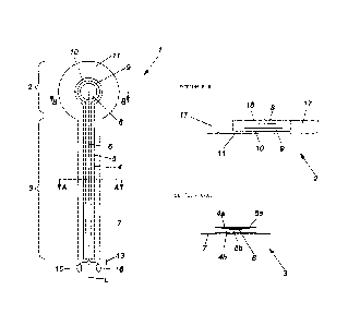
Fig. 1 shows a medical electrode 1, which comprises an electrode head 2, a
feed line 3
.. and a connecting plug 13 (with in this case projecting pins 16). According
to Fig. 1 the
substrate element 7 of the feed line 3 and the substrate element 11 of the
electrode
head 2 are formed in one piece, onto which the shielding plies 4 and 10 are
printed as
the next layer. The dielectric elements 5 and 9 are then printed on, followed
by the
electric conductor 6 and the signal transmitting and receiving layer 8.
A schematic cross-section in the region of the feed line 3 is shown in the
section A-A,
wherein firstly the lower shielding ply 4b and the lower dielectric element 5b
are printed
onto the substrate element 7. The upper dielectric element 5a and the upper
shielding
ply 4a are printed over the then applied electric conductor 6.
The essential components of the electrode head 2 can be seen schematically in
cross-
section in the section B-B, wherein the shielding layer 10, the dielectric
element 9 and
the signal transmitting and receiving layer 8 are printed onto the substrate
element 11.
In the lateral region these printed-on layers are bounded for example by a
foamed
material 17. To provide a better current conduction a gel 18 may be applied to
the
electrode head 2, as is known per se.
It should be noted in principle that in the drawings the interface between the
electrode
head 2 and feed line 3 is merely indicated. This interface where the electric
conductor
6 is no longer covered by the upper dielectric element 5a or by the upper
shielding ply
4a and can thus act without this protection as a signal transmitting and
receiving layer
8, is described in words.
CA 02823543 2013-07-02
=
7
Fig. 2 shows in principle a section through a round shielded cable 23 already
used in
medical electrodes, with an electric conductor 6, a dielectric element 5,
shielding 4 and
optionally a protective sleeve 12.
Since in addition to the handling the fabrication in particular of such a
known shielded
cable 23 is relatively complicated and disadvantageous, according to the
invention it is
envisaged that the feed line 3 comprises an elongated substrate element 7 onto
which
at least a part of the electrically conductive shielding layer 4 is printed. A
particularly
preferred embodiment in this respect is shown in Fig. 3. In this case the
lower
shielding ply 4b is printed onto the substrate element 7 and the dielectric
element 5b is
printed on top of this. After the printing-on of the electric conductor 6 this
is overprinted
by the upper dielectric element 5a, whereby the electric conductor 6 is
completely
surrounded by the dielectric element 5 transverse to the longitudinal axis L,
since the
elements 5a and 5b are cohesively joined to one another at least over certain
regions.
The same also applies to the shielding plies 4a and 4b, which in turn
completely
surround the dielectric element 5 transverse to the longitudinal axis L.
Furthermore a
protective sleeve 12 can be applied for example by means of a lacquer spray,
according to the dotted lines. It is also possible for the substrate element 7
and the
lower shielding ply 4b to be designed in the form of a one-piece metalized
film. The
advantage of this is that only the upper shielding ply 4a has to be printed.
Fig. 4 shows an alternative embodiment of the present invention, in which no
separate
substrate element 7 is provided, but instead the lower dielectric element 5b
is formed
as substrate element 7.
In principle in all variants it should be possible that at least individual
layers (4b, 5a, 5b
and 6) are not applied in the printing method, but instead for example are
also
introduced as individual films between the other layers in the production
process (e.g.
in the form of an adhesive film or in the form of a wire).
Fig. 5 shows schematically a printing device 14, with which at least
individual layers of
the medical electrode 1 can be printed. In principle it should be possible for
the printing
to take place in an in-line method or also by ink-jet printing. A screen-
printing method
is however preferred, in which a sheet up to several square metres in size,
preferably
in the form of a plastic substrate element 7, is fed into the printing device
14. The
CA 02823543 2013-07-02
8
required basic components 20a and 20b are then applied to the substrate
element 7
and onto previously extruded further layers 4, 5 or 6, via a moveable screen
printing
element 21 and via the printer nozzles 19. The desired final shapes of the
feed line 3
and electrode head 2 are of course already taken into account in the printing,
whereby
as the simplest variant the feed line 3 is printed on as a straight, elongated
element
and the electrode head 2 is printed on as a relatively compact element.
As an alternative a plan view of a substrate element 7 after the printing is
shown in Fig.
6, wherein in the upper region a relatively long feed line cable 3 is printed
with the
layers 4, 5 and 6, wherein after the printed components have dried a
relatively long
feed line cable can be formed by means of a corresponding blank 22 cut out as
illustrated by the shears. In a similar way and manner a spiral-shaped print
and blank
¨ as illustrated in the lower part of Fig. 6 ¨ can lead to a relatively long
feed line cable
3. In principle however it is preferably envisaged that the feed line cable 3
is relatively
straight and has a length between 30 and 150 cm, preferably between 50 and 100
cm.
Multiple electrodes 15 are illustrated in Fig.? and 8, in which a plurality of
separate
layers 4, 5 and 6 and 8,9 and 10 are applied to a substrate element 7 and 11.
An only very slightly extensible plastic material, such as for example a
polyester (in
particular PET), is preferably used as substrate element 7 and 11. It is
however also
possible to use a metalized film or even a polystyrene film as substrate
element 7 and
11.
Carbo inks or metal inks (for example copper or silver inks) are used as
shielding layer
4 and 10. These can be printed fully (over the whole surface) or in the manner
of a
grid.
In the printing method any suitable lacquer that is non-conductive and free
from pores
can be used as dielectric element 5 and 9.
The electric conductor 6 is produced, preferably printed, as a silver
conductor. The
signal receiving and transmitting layer 8 can also be applied in the form of a
silver
chloride layer. Tin and tin chloride can in principle also be used.
CA 02823543 2013-07-02
=
9
It should also be noted that in virtually all printed components 20a and 20b
various
additives such as lacquer elements, binders, solvents, etc are present, in
order to
ensure a friction-less printing procedure and to be able to produce functional
layers that
adhere well to one another.
Accordingly, the invention can be summarised as being based on replacing
(shielded)
feed line cables by a printed shielded feed line, wherein ideally this is
produced
(=printed) together with the electrode head (sensor region) in one production
procedure. This has advantages especially as regards the subsequent assembly
and
installation. In particular the very complicated assembly of a plug
integrating the
shielding for the connection to the device, which is necessary in the case of
shielded
round cables, but also even in the hypothetical installation of such a cable
on an
electrode in the sense that a shielding element of the electrode would its elf
have to be
electrically connected to the shielding of the cable, are radically simplified
by the
present invention.