Note: Descriptions are shown in the official language in which they were submitted.
CA 02823589 2013-08-09
DATA AND/OR COMMAND SIGNAL TRANSMISSION DEVICE
WITH ANTENNA ARRANGEMENTS
FIELD OF THE INVENTION
The invention concerns a device for transmitting data and/or
command signals, which uses a set of antennas, in particular of small
dimensions, for the combined transmission of said signals. This
transmission device is mainly used for transmitting long or medium wave
signals, such as, for example, for transponder systems.
BACKGROUND OF THE INVENTION
For data or command signal transmission, transmission antennas
must be capable of irradiating or radiating one or more electrical signals
with minimum losses and with a properly matched bandwidth. Thus, all the
spectral components of the electrical signals are radiated in the best
possible manner.
For small electrical antennas, namely antennas which have a much
smaller physical size than the transmission signal wavelength, it is
necessary to define a compromise between power loss and the bandwidth
of the signals to be transmitted. As a general rule, for small antennas with a
reasonable bandwidth, the product between power loss and signal
bandwidth must be constant. This property may also be explained by the
quality factor expression Q.
CA 02823589 2013-08-09
-2-
Some progress has already been made towards producing antennas
beyond this operating limit, but without attaining the hoped-for operation.
Thus, transmission antennas do not exist which are capable of radiating
electrical signals with a good quality factor Q taking into account the Chu
limit. The Chu limit for conventional antennas describes the minimum
quality factor, and consequently the maximum bandwidth, according to the
size of the conventional antenna. The Chu limit, well known for developing
said antennas, is based on the hypothesis that said antenna is passive,
linear and small.
To precisely determine this quality factor Q, reference may be made
to the article entitled "A re-examination of the fundamental limits on the
radiation Q of electrically small antennas" by J. S. McLean in the journal
IEEE transaction on antennas and propagation, 1996, vol. 44, issue 5.
Some small antenna embodiments are also described in the article entitled
"Electrically small super-directive and super-conductive antennas" by R.C.
Hansen in the 2006 work by Wiley, pages 62 to 84.
SUMMARY OF THE INVENTION
It is therefore an object of the invention to overcome the drawbacks
of the aforementioned state of the art by proposing a data and/or command
signal transmission device with small, high quality antennas, having a
bandwidth beyond the Chu limit and capable of transmitting electromagnetic
signals with a relatively low power loss.
The invention therefore concerns a data and/or command signal
transmission device, which includes the features defined in the independent
claim 1.
Specific embodiments of the data and/or command signal
transmission device are defined in the dependent claims 2 to 15.
CA 02823589 2013-08-09
-3-
One advantage of the data and/or command signal transmission
device lies in the fact that frequency switching for amplitude modulation of
the signals transmitted by the antenna arrangements is performed
synchronously with dynamic frequency adaptation of the resonance
frequency of the antenna arrangements.
Advantageously, the resonance frequency of at least one antenna
arrangement may be adapted by adding or removing a complementary
capacitor in parallel with a capacitor series-connected to an inductance and
a loss resistor. Synchronous frequency switching for data modulation is thus
performed at a zero voltage crossing across each capacitor. This allows the
use of loop antennas with a high quality factor Q and avoids any transitory
response during modulation state transition.
Advantageously, the transmission device of the present invention
produces cosine transition of symbols or of modulation states in the
modulated signals. This has an advantageous effect on the spectral
efficiency of the transmitted signals.
The invention therefore also concerns a method of actuating the data
and/or command signal transmission device, which includes the features
defined in the independent claim 16.
The invention therefore also concerns a method of actuating the data
and/or command signal transmission device, which includes the features
defined in the independent claim 17.
BRIEF DESCRIPTION OF THE DRAWINGS
The objects, advantages and features of the data and/or command
signal transmission device according to the invention, and the method of
activating the same will appear more clearly in the following description of
non-limiting embodiments illustrated by the drawings, in which:
CA 02823589 2013-08-09
-4-
Figure 1 is a general view of the various components of a data and/or
command signal transmission device according to the invention,
Figure 2 shows a temporal diagram of signals transmitted by the
antennas for data and/or command amplitude modulation of the data and/or
command signal transmission device according to the invention,
Figure 3 shows a first embodiment of the data and/or command
signal transmission device according to the invention,
Figure 4 shows a second embodiment of the data and/or command
signal transmission device according to the invention, and
Figures 5a and 5b show two comparative graphs of the data
amplitude modulation spectrum in signals transmitted by an antenna with
synchronous switching at the current crossing through 0 A and by antenna
arrangements according to the present invention.
DETAILED DESCRIPTION OF THE INVENTION
In the following description, all those elements of the data and/or
command signal transmission device that are well known to those skilled in
the art in this technical field will be described only in a simplified manner.
Figure 1 shows a simplified view of data and/or command signal
transmission device 1. This transmission device 1 can be used for
transmitting data and/or command signals to a set of transponders for a
sports competition, for example, or to radio stations. Each transponder
provided with a side antenna may be carried, in particular by a competitor,
in order to receive data from transmission device 1 of the present invention.
Preferably, the carrier frequency of the data and/or command signals
transmitted by transmission device 1 may be within the low frequency
range. The carrier frequency may be around 128 kHz. The transmitted data
rate in the signals may be around 16.5 kbit/s. The signals are transmitted
CA 02823589 2013-08-09
-5--
with a bandwidth of around 4 kHz, which is suitable for a transponder
system.
Transmission device 1 transmits data and/or command amplitude
modulation signals. The amplitude modulation may be ON-OFF keying or at
two amplitude levels for amplitude shift keying. To achieve this, the data
and/or command amplitude modulation may be performed immediately via
two or three antennas A1, A2, A3 of the transmission device by combining
or adding signals transmitted by each antenna. The antennas are controlled
independently of each other. Overlaying the transmitted signals may be
destructive depending on the signal phase difference, which depends on
the data and/or command state to be transmitted. This means that
amplitude modulation of the data and/or command to be transmitted is
obtained by combining or adding the transmitted in-phase or out-of-phase
signals. Any transmission power loss is also reduced by using the set of
antennas, which, in addition to radiating the electromagnetic signals, act as
a modulator assembly for the data and/or command to be transmitted.
Generally, transmission device 1 includes a synchronisation circuit 2,
a first signal generator 3 for controlling a first antenna arrangement 6, a
second signal generator 4 for controlling a second antenna arrangement 7,
and a third signal generator 5 for controlling a third antenna arrangement 8.
An oscillator (not shown) is also provided for synchronously clocking the
three signal generators 3, 4, 5. The oscillator may form part of
synchronisation circuit 2, which in this case controls the three signal
generators, but preferably the oscillator is comprised in second signal
generator 4. If the oscillator is comprised in the second signal generator, a
synchronous clocking signal is delivered from second signal generator 4 to
first signal generator 3 and to third signal generator 5.
With no data and/or command amplitude modulation or in a stable
modulation state, all of the sinusoidal signals transmitted by antenna
arrangements 6, 7 and 8 are at the same carrier frequency f0. To perform
CA 02823589 2013-08-09
,
-6-
the data and/or command amplitude modulation, the frequency of the
signals delivered by the first and third generators 3, 5, is temporarily
modified relative to the carrier frequency of the signals of second signal
generator 4 during each modulation state transition. The frequency change
in the signals delivered by the first and third signal generators 3, 5 occurs
temporarily during the transition phase from a first state to a second data
and/or command modulation state. A first state may define a "1" state, while
a second state may define a "0" state or vice versa.
During each modulation state transition phase, the signals delivered
to the first antenna arrangement 6 by first signal generator 3 are temporarily
at a frequency equal to f1=f0-Af for a certain number of signal cycles of the
signals of second signal generator 4, which remain at a carrier frequency
equal to f0. The signals delivered to the third antenna arrangement 8 by
third signal generator 5 are also temporarily at a frequency equal to
f3=f0+Af for a certain number of cycles of the signals of second signal
generator 4. After this certain number of cycles, the frequency of the signals
delivered by the three generators is re-set to the same carrier frequency f0.
Synchronisation circuit 2, explained in more detail below with
reference to Figures 3 and 4, is arranged to control the synchronous
switching of signals delivered by the signal generators. To achieve this,
frequency fl must be equal to f0.(n-0.5)/n, while frequency 13 must be equal
to f0.(n+0.5)/n, where n is an integer number defining the number of cycles
at frequency f0 for each modulation state transition phase. For a carrier
frequency f0 selected at 128 kHz, the number n must be equal to 8, which
gives a first frequency fl equal to 120 kHz and a third frequency f3 equal to
136 kHz. The ratio fO/Af may also be defined as equal to N, which is an
even integer number, where it is necessary to count N/2 cycles at frequency
f0 of the signals delivered by second signal generator 7 for each modulation
state transition phase.
CA 02823589 2013-08-09
-7-
To generate a second modulation state "0", the signals transmitted
by the first and third antenna arrangements 6 and 8 must, in principle, have
a phase difference of 1800 relative to the signals transmitted by the second
antenna arrangement 7. Conversely, to generate a first modulation state
"1", all the signals transmitted by antenna arrangements 6, 7 and 8 are in-
phase. Preferably, the amplitude of the signals transmitted by first antenna
arrangement 6 and third antenna arrangement 8 may be adapted to half the
amplitude of the signals transmitted by the second antenna arrangement 7.
Thus, with a 180 phase difference of the signals transmitted by the first
and third antenna arrangements 6 and 8 relative to the signals transmitted
by the second antenna arrangement 7, the combination or addition of the
three transmitted signals becomes zero after the transition phase from a
first state "1" to second state "0".
Figure 2 shows the signals transmitted by antennas A1, A2, A3 of the
three antenna arrangements 6, 7, 8, which are normally sinusoidal signals,
and the combined signals SD, in which data amplitude modulation is carried
out. It may be noted in Figure 2 that the amplitude of the combined data
signals SD is maximum when the three signals transmitted by the antennas
are in-phase, whereas the amplitude becomes zero when the signals
transmitted by antenna 1 and antenna 3 are out-of-phase by 180 from the
signals transmitted by antenna 2. It is therefore possible to define a first
modulation state "1" and a second modulation state "0" by combining the
three signals transmitted by the transmission device antennas. Each
modulation state transition phase may also be noted, particularly for the
change from a "1" state to a "0" state, and for the change from a "0" state to
a "1" state after 8 signal cycles of the second antenna are counted.
Of course, it is also possible to envisage using only two antennas A1
and A2 to perform data amplitude modulation. In these conditions, only two
signal generators, respectively connected to two antenna arrangements,
are required. Preferably, the signal amplitude of each antenna may be
identical, which produces a "1" state, when the two signals transmitted by
CA 02823589 2013-08-09
-8-
the two antennas are in-phase and a "0" state when the two signals
transmitted by the two antennas are out-of-phase by 180 .
It should also be noted that the amplitude of the first and third signals
of antennas A1 and A3 may be different from half the amplitude of the
signals of antenna A2. However, the amplitude resulting from the addition of
the first and third signals of antennas A1 and A3 must still be equal to or
less than the amplitude of the antenna A2 signals, even if the amplitude of
the antenna A1 signals is also different from the amplitude of the antenna
A3 signals.
In principle, detection of the combined data amplitude modulation
signals SD, as shown, is properly picked up by a receiver device, such as a
transponder, at a distance of at least 2, 10 or 15 m. The loop antennas A1,
A2, A3 used for transmission device 1 of Figure 1 must be arranged to be
oriented in the same direction with their axes parallel to each other. The
dimension of each antenna in the plane may be identical and 60 cm by 60
cm or with a diameter of around 60 cm.
Each loop antenna, not shown, may comprise 14 turns of an
insulated wire winding to obtain an inductance of around 370 pH. A space
of 1 mm may be set between each insulated wire. The maximum current
through each antenna may be around at least 1.2 A, or up to 2.5 A with a
field force generated at 10 m of around 66 dBpA/m. Transmission device 1
may be powered by a 5 V voltage source.
These antennas may be partly overlaid so that the inductive coupling
between antennas A1 and A2 and the inductive coupling between antennas
A2 and A3 is minimal. The antennas may also be arranged next to each
other in the same plane or also be arranged one on top of the other.
However, the dimension of the area occupied by the three antennas A1, A2
and A3 must generally be much smaller than the wavelength of the signals
transmitted by each antenna. For a carrier frequency f0 at 125 kHz for
CA 02823589 2013-08-09
-9-
example, the wavelength is around 2400 m. For close field transmission
applications, the area occupied by the three antennas A1, A2 and A3 must
be much smaller than the transmission distance or the magnetic/electrical
field measuring distance, which is set by national and international
standards.
In each stable modulation state, the resonance frequency of each
antenna arrangement 6, 7 and 8 is well defined as a function of the signals
delivered by each signal generator 3, 4 and 5 at a carrier frequency f0.
However, since the signal frequency is temporarily modified for the first and
third antenna arrangements 6 and 8, the resonance frequency must also be
dynamically adapted during the modulation state transition phase for each
of these antenna arrangements 6 and 8. By dynamically and synchronously
adapting the resonance frequency of the first and third antenna
arrangements 6 and 8 relative to the phase of the signals at carrier
frequency fO, it is possible to make each antenna arrangement with a high
quality factor Q. This high quality factor Q may be higher than 100 to
simultaneously keep a bandwidth much higher than 10%. This reduces
power losses particularly during each modulation state transition phase and
means there is no transitory response, if the antenna switching is performed
synchronously at a well defined moment.
In each antenna arrangement 6, 7 and 8, there may be inductive or
capacitive elements which can be combined to adapt the antenna
resonance frequency as a function of the frequency of the signals delivered
by each signal generator 3, 4 and 5. In principle, only the first antenna
arrangement 6 and the third antenna arrangement 8 include these
complementary inductive or capacitive elements for adapting the resonance
frequency during each modulation state transition phase.
The first antenna arrangement 6 may include, in series between the
output of the first signal generator 3 and an earth terminal, a loss resistor
R1, an inductance A1 defining the first antenna and at least a first capacitor
C11. A second capacitor C12 may be placed in parallel with first capacitor Cii
CA 02823589 2013-08-09
-10-
of the first antenna arrangement via a first switch 9 to adapt the resonance
frequency. This first switch is controlled synchronously by a first command
signal STi of synchronisation circuit 2. This first switch may be
conventionally formed of a MOS transistor, such as an NMOS transistor,
whose source and drain terminals are connected between a terminal of the
second capacitor C12 and the earth terminal. The gate terminal of this
NMOS transistor is arranged to receive the first command signal STi. If this
first command signal ST1 is at the high state, the NMOS transistor is made
conductive and second capacitor C12 is placed in parallel to first capacitor
C11. However, if this first command signal ST is at the low state, for example
at 0 V, the NMOS transistor is non-conductive and only the first capacitor
C11 is series-connected to inductance A1 and loss resistor R1.
The second antenna arrangement 7 may simply include, in series
between the output of the second signal generator 4 and an earth terminal,
a loss resistor R2, an inductance A2 defining the second antenna and at
least one capacitor C21. It is not necessary for this second antenna
arrangement 7 to adapt the resonance frequency during the modulation
state transition phase. The elements which form this second antenna
arrangement 7 are initially determined so that the resonance frequency
matches the carrier frequency f0 of the signals delivered by second signal
generator 4.
The third antenna arrangement 8 may include, in series between the
output of the third signal generator 5 and an earth terminal, a loss resistor
R3, an inductance A3 defining the third antenna and at least a first
capacitor C3i. A second capacitor C32 may be placed in parallel to the first
capacitor C31 of the third antenna arrangement via a second switch 10 to
adapt the resonance frequency. This second switch is controlled
synchronously by a second command signal ST, which is the inverse of the
first command signal STI. The second command signal is delivered by
synchronisation circuit 2. This second switch 10 may, like first switch 9, be
formed of a MOS transistor, such as an NMOS transistor, whose source
CA 02823589 2013-08-09
-I l-
and drain terminals are connected between a terminal of second capacitor
C32 of third antenna arrangement 8 and the earth terminal. The gate
terminal of this NMOS transistor is arranged to receive the second
command signal ST. If this second command signal ST is at the high state,
the NMOS transistor is made conductive and second capacitor C32 is
placed in parallel to first capacitor C31. However, if this second command
signal ST is at the low state, for example at 0 V, the NMOS transistor is non-
conductive and only the first capacitor C31 is series-connected to inductance
A3 and loss resistor R3.
By way of numerical example, loss resistors R1, R2 and R3 may each
be set at a resistive value equal to 3 Ohms. Each inductance A1, A2 and A3
may have a value of 370 pH. The first capacitor C11 of first antenna
arrangement 6 may have a capacitive value equal to 4.183 nF, just like
capacitor C21 of second antenna arrangement 7. The second capacitor C12
of first antenna arrangement 6 may have a capacitive value equal to 576
pF. The first capacitor C31 of third antenna arrangement 8 may have a
capacitive value equal to 3.705 nF, and second capacitor C32 of third
antenna arrangement 8 may have a capacitive value equal to 478 pF.
These numerical values are defined for transmission device 1 to operate
with signals transmitted at a carrier frequency f0 equal to 128 kHz, and for
temporarily modified frequencies of the first and third antenna
arrangements 6 and 8 equal to 120 kHz and 136 kHz. For the modified
frequencies, the first switch 9 is temporarily closed to have a capacitive
value of 4.759 nF with first capacitor C11 placed in parallel to second
capacitor C12, whereas the second switch 10 is open with a capacitive value
of 3.705 nF of first capacitor C31.
Wheneach modulation state is properly set after each modulation
state transition phase, the signals transmitted by the three antennas A1, A2
and A3 are at a carrier frequency fO, which may be equal to 128 kHz. In
each stable modulation state, the first switch 9 is still opened by the first
command signal STi delivered by synchronisation circuit 2, whereas the
CA 02823589 2013-08-09
-12-
second switch 10 is still closed, as it is controlled by the second command
signal ST. However, during the modulation state transition phase, the first
switch 9 is temporarily closed, whereas the second switch 10 is temporarily
open. To be able to switch the frequencies of the signals delivered by the
first and third signal generators 3 and 5, the switching must be performed
synchronously and at the right moment with respect to the phase of the
signals at carrier frequency fO, to avoid any transitory response.
The modulation state transition phase may last for 8 sinusoidal signal
cycles of second antenna arrangement 7. By adapting the resonance
frequency of the first and third antenna arrangements 6 and 8, each
frequency switch of the signals delivered by the first and third signal
generators 3 and 5 must be performed synchronously by detecting the zero
crossings of the sinusoidal signals of the second antenna arrangement. To
achieve this, the connection node between inductance A2 and capacitor C21
of second antenna arrangement 7 is connected to synchronisation circuit 2,
which includes a zero voltage crossing detector. The resonance frequency
must be adapted at the moment when the voltage across capacitor C21 of
second antenna arrangement 7 is at 0 V, with no stored electrical energy to
prevent any transitory response. At the same moment, the voltage at the
start and at the end of each transition phase across each of capacitors Ci
and C31 must necessarily be at 0 V.
Each zero crossing detected by the detector may be counted by a
counter in the synchronisation circuit to control the closing or opening of
the
first and second switches 9 and 10. Likewise, the first command signal ST1
may be used to control the frequency switch of the first and third signal
generators 3 and 5. The frequency switch of antenna arrangements 6 and 8
also occurs at the zero crossing of the signals transmitted by first antenna
A1 and third antenna A3. However, the frequency switch occurs once with
a 1800 phase difference relative to the signals of second antenna
arrangement 7 for the second modulation sate, and in-phase for the first
modulation state. Thus, each modulation state transition is performed
CA 02823589 2013-08-09
-13-
synchronously with dynamic modification of each resonance frequency of
the antenna arrangements. This allows a continuous and muted transition
to be performed with no power loss by a crossing of the disengaged cosine
or raised cosine type from one modulation state to another. However, with
two antennas, the modulation state transition on the 00K modulation
signals cannot be cosine shaped, but with a change, which introduces a
"fold" in the transmitted modulation signals. This results in very poor
behaviour in terms of spectral efficiency.
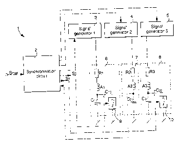
Figure 3 shows a first slightly more detailed embodiment of
transmission device 1. It should be noted that elements in Figure 3 that are
the same as those in Figure 1 bear identical reference signs. Consequently,
for the sake of simplification, the description of all these elements will not
be
repeated. The resonance frequency of the first and third antenna
arrangements 6 and 8 is adapted in a capacitive manner as in the general
embodiment shown in Figure 1. To achieve this, a second complementary
capacitor C12, C32 can be placed in parallel to a first capacitor C11, C31 via
a
first switch 9 or a second switch 10, controlled inversely.
The second signal generator 4 preferably includes an oscillator 40
capable of generating an oscillating signal at a frequency which may be
chosen to be higher than the MHz, for example at 32.64 MHz. The
oscillating signal may be sinusoidal, but is preferably formed of rectangular
pulses. The oscillating signal frequency is divided in a frequency divider 41,
which thus delivers a divided frequency signal to a drive circuit 42. On basis
of the divided frequency signal, drive circuit 42 delivers determined
frequency signals to second antenna arrangement 7. The determined
frequency may be a carrier frequency f0 equal for example to 128 kHz. In
these conditions, frequency divider 41 has to divide the oscillating signal by
a factor equal to 255.
It should be noted that it is also the task of drive circuit 42 to adapt the
amplitude of the signals transmitted by antenna A2 of second antenna
arrangement 7. To achieve this, drive circuit 42 may be controlled by a
CA 02823589 2013-08-09
-14-
processing unit with a microprocessor (not shown). Drive circuit 42 may be
formed of a non-linear amplifier or may also include a well known pulse
width modulator. This pulse width modulator is controlled by the
microprocessor processing unit based on a voltage or current measurement
taken at the output of drive circuit 42, until the desired amplitude is
obtained
for the signals transmitted by antenna A2.
The first signal generator 3 is formed of a programmable frequency
divider 31 followed by a drive circuit 32, which delivers the adapted
frequency signals to first antenna arrangement 6. The frequency divider
receives the oscillating signal from an oscillator 40 of the second signal
generator 4. On the basis of this oscillating signal, frequency divider 31
divides the oscillating signal frequency by factor 255, when a stable data
modulation state is defined or when no data modulation is performed.
However, during a modulation state transition phase for the change from a
"1" state to a "0" state, or vice versa, the oscillating signal frequency is
divided by factor 272. In this manner, drive circuit 32 delivers" signals at a
frequency temporarily equal to 120 kHz to first antenna arrangement 6. The
first command signal STõ delivered by synchronisation circuit 2, may be
used to control the change in division factor of frequency divider 31.
The third signal generator 5 is formed of a programmable frequency
divider 51 followed by a drive circuit 52, which delivers the adapted
frequency signals to third antenna arrangement 8. The frequency divider
receives the oscillating signal from oscillator 40 of the second signal
generator 4. On the basis of this oscillating signal, frequency divider 51
divides the oscillating signal frequency by factor 255, when a stable data
modulation state is defined or when no data modulation is performed.
However, during a modulation state transition phase for the change from a
"1" state to a "0" state, or vice versa, the oscillating signal frequency is
divided by factor 240. In this manner, drive circuit 52 delivers signals at a
frequency temporarily equal to 136 kHz to third antenna arrangement 8.
CA 02823589 2013-08-09
-15-
The first command signal STi, delivered by synchronisation circuit 2, may
also be used to control the change in division factor of frequency divider 51.
It should be noted that the division factor of each frequency divider 31,
41, 51 may be determined according to the desired carrier frequency f0 and
the frequency deviation Af. For a division factor equal to N, which is an
integer number, the divided signals at the frequency dividers' output are at a
carrier frequency f0 determined according to the frequency of the oscillating
signal from the oscillator. For the signals at frequency f0-Af for the first
antenna arrangement 6, the division factor of frequency divider 31 is equal
to N.(1+Af/f0). For the signals at frequency f0+Af for the third antenna
arrangement 6, the division factor of frequency divider 51 is equal to N.(1-
Af/f0).
Drive circuits 32 and 52 of the first and third signal generators 3 and 5,
may also be controlled by the microprocessor processing unit to adapt the
amplitude of the signals transmitted by the first and third antenna
arrangements 6 and 8. The amplitude of the signals of the first and third
antenna arrangements 6 and 8 may be adapted to be half the amplitude of
the signals of the second antenna arrangement 7.
Synchronisation circuit 2 includes a first D-type flip-flop 21 for
receiving at input the modulation signal Smod, which may be formed of
rectangular pulses representing the data or at least one command to be
transmitted. The non-inverted output Q of the first flip-flop 21 is connected
to a first input of an Exclusive-OR gate 23, while the inverted output Qb of
the first flip-flop is connected to the input of a counter-by-n 22, where n is
an integer number greater than 1. The output of counter 22 is connected to
a second input of the Exclusive-OR gate 23. The output of this Exclusive-
OR gate 23 is connected to the input of a second D-type flip-flop 24, which
is capable of delivering, in particular, the first command signal STi at an
inverted output Qb and the second command signal ST at a non-inverted
output Q. These command signals ST and STi are thus partly used to control
CA 02823589 2013-08-09
-16-
the opening or closing of switches 9 and 10 of antenna arrangements 6 and
8.
The first and second D-type flip-flops 21 and 24 are clocked by a
clocking signal from a zero crossing detector 25. Zero crossing detector 25
detects the zero crossings of the sinusoidal voltage at the connection node
between inductance A2 and capacitor C21 of the second antenna
arrangement 7. This sinusoidal voltage represents the shape of the signals
transmitted from second antenna arrangement 7. The sinusoidal voltage is
thus converted via zero crossing detector 25 into a clocking signal formed of
successive rectangular pulses at the same frequency f0 as the sinusoidal
voltage.
Counter-by-n 22 is normally also clocked on the basis of the rising
edges of the clock pulses delivered by zero crossing detector 25. When
there is a change of state at inverted output Qb of first flip-flop 21, the
new
state of output Qb is only transmitted at the output of counter 22 after n
clocking pulses have been delivered by zero crossing detector 25. These n
pulses match the number n of cycles of the sinusoidal voltage across
capacitor C21 or of the signals transmitted by antenna A2 of second
antenna arrangement 7. During a period matching n clocking pulses, the
Exclusive-OR gate only delivers a "0" state to the input of the second flip-
flop 24. The first command signal STi at the inverted output Qb of second
flip-flop 24 is thus at a high "1" level for the duration of n clocking
pulses,
which correspond to the modulation state transition phase. During this
modulation state transition phase, the resonance frequencies of first
antenna arrangement 6 and of third antenna arrangement 8 are adapted as
a function of the modified frequencies of the signals delivered by the first
and third signal generators 3 and 5.
Figure 4 shows a second, more detailed embodiment of transmission
device 1. It should be noted that any elements in Figure 4 which are the
same as those in Figures 1 and 3 bear identical reference signs.
Consequently, for the sake of simplification, the description of all these
CA 02823589 2013-08-09
-17-
elements will not be repeated. The resonance frequency of the first and
third antenna arrangements 6 and 8 is adapted in a capacitive manner as
for the general embodiment shown in Figure 1 and the first embodiment
shown in Figure 3.
The second signal generator 4 preferably includes an oscillator 40
capable of generating an oscillating signal at a frequency which matches
the carrier frequency of the signals to be transmitted by second antenna
arrangement 7. The oscillating signal frequency may thus be selected for
example to be at 128 kHz, like the carrier frequency f0 of the signals to be
transmitted by second antenna arrangement 7. The oscillating signal may
be of sinusoidal shape, but preferably formed of rectangular pulses
delivered straight to drive circuit 42. Drive circuit 42 thus delivers the
signals
at carrier frequency f0 to second antenna arrangement 7.
The second signal generator 4 also includes a frequency multiplier 43
directly connected to oscillator 40. This frequency multiplier is used to
multiply the oscillating signal frequency by a factor n1, which is an integer
number greater than 1. The multiplied frequency signal in frequency
multiplier 43 is delivered to the first and third signal generators 3 and 5.
Where the carrier frequency f0 of the signals to be transmitted by antenna
A2 is selected to be 128 kHz, the multiplication factor n1 may be selected to
be equal to 255.
The first signal generator 3 includes first and second frequency
division branches for the multiplied frequency signal received from
frequency multiplier 43. In the first division branch, the frequency is
divided
by factor n1 so as to deliver signals at carrier frequency f0 at the output of
the first signal generator 3. In the second division branch, the frequency is
divided by a factor n2, which is an integer number greater than 1. This
factor n2 is selected so that the first signal generator temporarily delivers
signals to first antenna arrangement 6 at frequency f1-40-Af, during the
modulation state transition phase. Frequency fl is therefore determined by
CA 02823589 2013-08-09
-18-
fO=nl/n2. To obtain frequency fl equal to 120 kHz for example, factor n2
must be equal to 272.
The first signal generator 3 thus includes for the first division branch, a
first inverter 30, which receives the first command signal Sri from
synchronisation circuit 2. This first command signal ST1 is at the "1" state
during the modulation state transition phase and at the "0" state for each
stable modulation state before and after the transition phase. The first
branch is therefore used when the first command signal ST1 is at the "0"
state, while the second branch is used when the first command signal ST1 is
at the "1" state.
The output of first inverter 30 of the first branch is connected to a first
input of a first AND gate 33, which receives at a second input the multiplied
frequency signal from frequency multiplier 43. The multiplied frequency
signal is transmitted to a first counter-by-n1 35, if the output of first
inverter
30 is at the "1" state. This enables the frequency of the multiplied frequency
signal to be divided by factor n1. The output of first counter 35 is connected
to a second AND gate 37 which receives, at a second input, the output
signal from first inverter 30. The output of the second AND gate 37 is
connected to a first input of an OR gate 39 to deliver the carrier frequency
signal f0 to drive circuit 32. The configuration of drive circuit 32 is
similar to
that of Figure 3 so as to deliver signals at carrier frequency f0 to first
antenna arrangement 6 other than during the modulation state transition
phase.
For the second division branch, the first command signal STi is
delivered directly to a first input of a third AND gate 34, while the second
input of AND gate 34 receives the multiplied frequency signal from
frequency multiplier 43. The multiplied frequency signal is transmitted to a
second counter-by-n2 36, if the first command signal STi is at the "1" state.
This divides the frequency of the multiplied frequency signal by factor n2.
The output of second counter 36 is connected to a fourth AND gate 38,
which receives the first command signal STi at a second input. The output of
CA 02823589 2013-08-09
-19-
the fourth AND gate 38 is connected to a second input of OR gate 39 to
deliver the adapted frequency signal f1=f0-Af to drive circuit 32. This
adapted frequency fl may thus be equal to 120 kHz in this embodiment of
transmission device 1.
The third signal generator 5 also includes first and second frequency
division branches for the multiplied frequency signal received from
frequency multiplier 43. In the first division branch, the frequency is
divided
by factor n1 to output signals at carrier frequency f0 from the third signal
generator 5 to the third antenna arrangement 8. In the second division
branch the frequency is divided by a factor n3, which is an integer number
greater than 1. This factor n3 is selected so that the third signal generator
temporarily delivers signals to third antenna arrangement 8, at frequency
f3=f0+Af, during the modulation state transition phase. Frequency f3 is thus
determined by fO.n1/n3. To obtain frequency f3 equal to 136 kHz, for
example, factor n3 must be equal to 240.
The third signal generator 5 thus includes for the first division branch,
a second inverter 50, which receives the first command signal STi from
synchronisation circuit 2. This first command signal Sri is at the "1" state
during the modulation state transition phase and at the "0" state for each
stable modulation state before and after the transition phase. The first
branch is used when the first command signal S-ri is at the "0" state, while
the second branch is used when the first command signal ST1 is at the "1"
state.
The output of second inverter 50 of the first branch is connected to a
first input of a first AND gate 53, which receives at a second input the
multiplied frequency signal from frequency multiplier 43. The multiplied
frequency signal is transmitted to a first counter-by-n1 55, if the output of
second inverter 50 is at the "1" state. This enables the frequency of the
multiplied frequency signal to be divided by factor n1. The output of first
counter 55 is connected to a second AND gate 57 which receives, at a
second input, the output signal from second inverter 50. The output of the
CA 02823589 2013-08-09
-20-
second AND gate 57 is connected to a first input of an OR gate 59 to
deliver the carrier frequency signal f0 to drive circuit 52. The configuration
of
drive circuit 52 is similar to that of Figure 3 so as to deliver signals at
carrier
frequency f0 to third antenna arrangement 8 other than during the
modulation state transition phase.
For the second division branch, the first command signal ST1 is
delivered directly to a first input of a third AND gate 54, while the second
input of AND gate 54 receives the multiplied frequency signal from
frequency multiplier 43. The multiplied frequency signal is transmitted to a
second counter-by-n3 56, if the first command signal ST, is at the "1" state.
This enables the frequency of the multiplied frequency signal to be divided
by factor n3. The output of second counter 56 is connected to a fourth AND
gate 58, which receives the first command signal STi at a second input. The
output of the fourth AND gate 58 is connected to a second input of OR gate
59 to deliver the adapted frequency signal f3=f0+Af to drive circuit 52. This
adapted frequency f3 may thus be equal to 136 kHz in this embodiment of
transmission device 1.
It should be noted that synchronisation circuit 2 includes the same
elements as those described above with reference to Figure 3. However,
first flip-flop 21 may be clocked directly by the oscillating signal from
oscillator 40, while the second flip-flop 24 remains clocked by the
rectangular pulsed signal delivered by zero crossing detector 25.
Figures 5a and 5b show two comparative graphs of the data amplitude
modulation spectrum in the signals transmitted by a single antenna and by
antenna arrangements according to the present invention. It is to be noted
that with the transmission device of the present invention and the
alternative principle using a set of antennas, harmonic frequencies are
greatly reduced relative to the central frequency, which in this case is at
128
kHz. The magnetic field force of the transmission principle using three
antenna arrangements of the invention is thus within the spectral mask of
regulatory requirements according to the field of application, such as the
CA 02823589 2013-08-09
-21-
field of sport. With amplitude modulation signal transmission using a single
antenna, numerous harmonics occur which fall outside the required spectral
mask.
From the description that has just been given, several variants of the
data and/or command signal transmission device, and the method of
activating the transmission device, can be devised by those skilled in the art
without departing from the scope of the invention defined by the claims. Six
antenna arrangements respectively controlled by six signal generators could
be used. Three first antenna arrangements may transmit data and/or
command signals as described above, and three second antenna
arrangements, with the same configuration as the three first antenna
arrangements, transmit signals with a 900 phase difference. Where the
resonance frequency is adapted using a complementary inductance, a peak
detector or minima/maxima crossing detector may be used to control the
synchronisation circuit. Each frequency switch must occur in each
modulation state transition phase when the current in the inductance of the
second antenna arrangement and in the adapted inductances of the other
antenna arrangements is equal to 0 A.